EP1619551A2 - Methode zur Herstellung einer Membranmaske, Methode zur Herstellung eines Halbleiterbauelements und Membranmaske - Google Patents
Methode zur Herstellung einer Membranmaske, Methode zur Herstellung eines Halbleiterbauelements und Membranmaske Download PDFInfo
- Publication number
- EP1619551A2 EP1619551A2 EP05002943A EP05002943A EP1619551A2 EP 1619551 A2 EP1619551 A2 EP 1619551A2 EP 05002943 A EP05002943 A EP 05002943A EP 05002943 A EP05002943 A EP 05002943A EP 1619551 A2 EP1619551 A2 EP 1619551A2
- Authority
- EP
- European Patent Office
- Prior art keywords
- electron beam
- membrane
- mask
- exposure apparatus
- beam exposure
- Prior art date
- Legal status (The legal status is an assumption and is not a legal conclusion. Google has not performed a legal analysis and makes no representation as to the accuracy of the status listed.)
- Withdrawn
Links
- 239000012528 membrane Substances 0.000 title claims abstract description 202
- 238000004519 manufacturing process Methods 0.000 title claims abstract description 29
- 239000004065 semiconductor Substances 0.000 title claims description 20
- 238000010894 electron beam technology Methods 0.000 claims abstract description 86
- 230000000295 complement effect Effects 0.000 claims abstract description 69
- 239000000463 material Substances 0.000 claims abstract description 43
- 230000035945 sensitivity Effects 0.000 claims description 17
- 230000001133 acceleration Effects 0.000 claims description 9
- 238000002834 transmittance Methods 0.000 description 38
- 230000007423 decrease Effects 0.000 description 15
- 239000010408 film Substances 0.000 description 10
- 238000000034 method Methods 0.000 description 10
- 238000005516 engineering process Methods 0.000 description 6
- 238000001459 lithography Methods 0.000 description 6
- 230000003247 decreasing effect Effects 0.000 description 5
- 238000001803 electron scattering Methods 0.000 description 4
- 235000012489 doughnuts Nutrition 0.000 description 3
- OKTJSMMVPCPJKN-UHFFFAOYSA-N Carbon Chemical compound [C] OKTJSMMVPCPJKN-UHFFFAOYSA-N 0.000 description 2
- VYPSYNLAJGMNEJ-UHFFFAOYSA-N Silicium dioxide Chemical compound O=[Si]=O VYPSYNLAJGMNEJ-UHFFFAOYSA-N 0.000 description 2
- XUIMIQQOPSSXEZ-UHFFFAOYSA-N Silicon Chemical compound [Si] XUIMIQQOPSSXEZ-UHFFFAOYSA-N 0.000 description 2
- 230000008901 benefit Effects 0.000 description 2
- 229910052799 carbon Inorganic materials 0.000 description 2
- 238000010586 diagram Methods 0.000 description 2
- 238000007689 inspection Methods 0.000 description 2
- 239000002245 particle Substances 0.000 description 2
- 229910052710 silicon Inorganic materials 0.000 description 2
- 239000010703 silicon Substances 0.000 description 2
- 238000012546 transfer Methods 0.000 description 2
- 229910004012 SiCx Inorganic materials 0.000 description 1
- 229910004205 SiNX Inorganic materials 0.000 description 1
- 229910003481 amorphous carbon Inorganic materials 0.000 description 1
- 229910021417 amorphous silicon Inorganic materials 0.000 description 1
- 238000004458 analytical method Methods 0.000 description 1
- 230000015572 biosynthetic process Effects 0.000 description 1
- 229910052681 coesite Inorganic materials 0.000 description 1
- 229910052906 cristobalite Inorganic materials 0.000 description 1
- 230000007547 defect Effects 0.000 description 1
- 238000001514 detection method Methods 0.000 description 1
- 238000011161 development Methods 0.000 description 1
- 229910003460 diamond Inorganic materials 0.000 description 1
- 239000010432 diamond Substances 0.000 description 1
- 238000009826 distribution Methods 0.000 description 1
- 230000000694 effects Effects 0.000 description 1
- 238000000609 electron-beam lithography Methods 0.000 description 1
- 238000005530 etching Methods 0.000 description 1
- 238000003384 imaging method Methods 0.000 description 1
- 238000011835 investigation Methods 0.000 description 1
- 238000012986 modification Methods 0.000 description 1
- 230000004048 modification Effects 0.000 description 1
- 230000002093 peripheral effect Effects 0.000 description 1
- 238000000206 photolithography Methods 0.000 description 1
- 238000012545 processing Methods 0.000 description 1
- 238000012827 research and development Methods 0.000 description 1
- 239000000377 silicon dioxide Substances 0.000 description 1
- 230000003068 static effect Effects 0.000 description 1
- 229910052682 stishovite Inorganic materials 0.000 description 1
- 239000010409 thin film Substances 0.000 description 1
- 229910052905 tridymite Inorganic materials 0.000 description 1
Images


Classifications
-
- G—PHYSICS
- G03—PHOTOGRAPHY; CINEMATOGRAPHY; ANALOGOUS TECHNIQUES USING WAVES OTHER THAN OPTICAL WAVES; ELECTROGRAPHY; HOLOGRAPHY
- G03F—PHOTOMECHANICAL PRODUCTION OF TEXTURED OR PATTERNED SURFACES, e.g. FOR PRINTING, FOR PROCESSING OF SEMICONDUCTOR DEVICES; MATERIALS THEREFOR; ORIGINALS THEREFOR; APPARATUS SPECIALLY ADAPTED THEREFOR
- G03F1/00—Originals for photomechanical production of textured or patterned surfaces, e.g., masks, photo-masks, reticles; Mask blanks or pellicles therefor; Containers specially adapted therefor; Preparation thereof
- G03F1/20—Masks or mask blanks for imaging by charged particle beam [CPB] radiation, e.g. by electron beam; Preparation thereof
Definitions
- the invention relates to a mask for electron beam exposure, and more particularly, to a method of manufacturing a membrane mask, a method of manufacturing a semiconductor device, and a membrane mask.
- Lithography technology which supports the advancement of shrinking in semiconductor devices, is a critical process among other semiconductor manufacturing processes in that it is the only process for producing patterns.
- optical lithography has been used in producing semiconductor devices.
- pattern critical dimensions of advanced devices are approaching the limit resolution. It is thus urgent to develop high-resolution lithography.
- Electron beam lithography has inherently superior resolution property, and has been partly used for developing and for producing most advanced devices typified by SOC (system on chip).
- SOC system on chip
- the wafer processing capacity per unit time, or throughput is low because the pattern is delineated with one stroke . It is thus unsuitable to mass production of devices.
- EPL Electron Projection Lithography
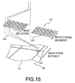
- Fig. 15 is a conceptual diagram for illustrating the operation of an EPL exposure apparatus.
- masks 340 are arranged on a mask stage in the EPL exposure apparatus.
- subfield masks 350 are formed and aligned in a grid.
- a subfield pattern is formed for projecting and transferring a subfield 320 served as an exposure unit area for one semiconductor chip.
- the subfield 320 is an area corresponding to one shot of exposure with electron beam 330 (charged particle beam).
- electron beam 330 charged particle beam
- various subfield patterns transmitting the electron beam 330 are formed, respectively.
- the electron beam 330 emitted from the charged particle source is deflected by a deflector, with which a pattern of a predetermined subfield mask 350 is irradiated.
- a subfield 320 served as an exposure unit area in one semiconductor chip area among a plurality of semiconductor chip areas 310 reduced by an electron lens and partitioned on the wafer 300, is irradiated with the transmitted electron beam 330 to project and transfer the subfield pattern formed in the subfield mask 350.
- the electron beam 330 is deflected by the deflector so that the subfield pattern of a subfield mask 350 located in the next line is irradiated with the electron beam 330.
- the next subfield 320 for the above-mentioned one semiconductor chip is irradiated to project and transfer a subfield pattern formed in the subfield mask 350 to the next subfield 320.
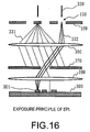
- Fig. 16 illustrates the exposure principle of EPL.
- a stencil mask 100 as an example of a scattering mask in which an opening pattern is formed by perforating openings 150, is irradiated with electrons accelerated at 100 kV.
- silicon Si
- Electron beam 330 incident on a portion other than the openings 150 of the stencil mask 100 is greatly scattered at the portion other than the openings 150.
- Most of the scattered electrons (mask-scattered electrons) 331 are blocked by a limiting aperture 370 placed at the back focal plane of the objective lens 380.
- image-forming electrons 332 transmitted through the opening 150 are projected by a projection lens 360 because they freely pass through the opening 150.
- Fig. 17 shows an example of a stencil mask and a membrane mask manufactured from typical material.
- Figs. 17A and 17B the pattern portion is particularly shown and the other portions are omitted.
- Fig. 17A shows an example stencil mask 100 made of Si with a thickness of 2 ⁇ m, for example.
- Fig. 17B shows a membrane mask 200 made of diamondlike carbon (DLC) membrane with a thickness of 30 to 50 nm, on which a patterned DLC scattering layer is formed with a thickness of about 600 nm.
- DLC diamondlike carbon
- Fig. 18 illustrates how electron transmits the aperture.
- Fig. 18A for the stencil mask 100, electrons incident on the opening 150 are passed without being scattered. Thus all of these electrons can contribute to exposure.
- Fig. 18B for the membrane mask 200, even the electrons incident on the opening pattern portion might be scattered by the membrane 210. The scattered electrons cannot reach the wafer 300. Only part of the electrons that are not scattered contribute to exposure (see, e.g., "High-performance membrane mask for electron projection lithography", H. Yamashita, I. Amemiya, E. Nomura, K. Nakajima, and H. Nozue, J. Vac. Sci. Technol. B 18, 3237 (2000)).
- Fig. 19 shows examples of complementary division of patterns.
- Fig. 19A shows an example of an opening pattern closed like a donut.
- a stencil mask 100 is used as a mask in the EPL exposure apparatus, the portion that electrons pass is completely perforated.
- the opening pattern is shaped like a donut, the mask member inside it will be dropped off.
- the pattern must be divided into two or more complementary masks.
- the mask is divided into a first complementary pattern 111 and a second complementary pattern 112 to prepare first and second complementary masks.
- Each of the complementary masks is placed in the EPL exposure apparatus.
- the first and second complementary masks are each exposed once, that is, exposure is performed in two iterations, to complete a pattern on the wafer.
- a pattern having insufficient mechanical strength in which a large mask member is supported by a small supporting portion must also be divided.
- Fig. 19B shows an example of a leaf-shaped opening pattern.
- Fig. 19C shows an L-shaped opening pattern.
- Fig. 20 shows the cross-sectional structure of a membrane mask.
- DLC has a high Young's modulus, and provides high film strength even when it is subjected to thinning. Moreover, thin film of good quality can be obtained because of its film growth.
- a DLC membrane mask 200 with a thickness of 15 to 50 nm is fabricated.
- a DLC membrane 210 with a thickness of 44 nm yields a transmittance of unscattered electrons of 41%.
- its scattering layer 230 is also made of DLC.
- it since it requires to scatter electrons, it has a thickness of about 600 nm, which is thicker than the membrane 210 (see, e.g., "Fabrication of a continuous diamondlike carbon membrane mask for electron lithography", I.
- membranes with a transmittance of unscattered electrons of 50% or more (70% in Fig. 17B) are manufactured.
- a beam current measuring area provided on the membrane mask is irradiated with electron beam, with the membrane mask being installed in the exposure apparatus.
- the current that reaches the wafer surface is measured.
- the exposure condition is determined from the measured current value and a set amount of exposure, thereby avoiding the decrease of throughput due to a membrane mask regardless of the membrane thickness of the membrane mask.
- the membrane mask requires no complementary division, and the number of exposure iterations is half of that for the stencil mask. However, if the transmittance is half or less, the membrane mask may have exposure throughput lower than the stencil mask.
- a method of manufacturing a membrane mask for use in an electron beam exposure apparatus that exposes resist material comprising: manufacturing the membrane mask with a membrane thickness determined so that an operation time that the electron beam exposure apparatus spends in exposing the resist material to form a predetermined pattern using the membrane mask is comparable to or less than an operation time that the electron beam exposure apparatus spends in exposing the resist material to form the predetermined pattern using complementary masks.
- a method of manufacturing a semiconductor device comprising the step of exposing resist material using a membrane mask by an electron beam exposure apparatus, wherein the membrane mask with a membrane thickness is used, the membrane thickness being determined so that an operation time that the electron beam exposure apparatus spends in exposing the resist material to form a predetermined pattern using the membrane mask is comparable to or less than an operation time that the electron beam exposure apparatus spends in exposing the resist material to form the predetermined pattern using complementary masks.
- a membrane mask used for exposing resist material by an electron beam exposure apparatus having a membrane thickness determined so that an operation time that the electron beam exposure apparatus spends in exposing the resist material to form a predetermined pattern using the membrane mask is comparable to or less than an operation time that the electron beam exposure apparatus spends in exposing the resist material to form the predetermined pattern using complementary masks.
- the overall exposure performance of EPL is improved by using a membrane mask with a membrane thickness optimized from parameters of the exposure apparatus in use and electron scattering parameters in the membrane.
- the membrane thickness is optimized by comparison with the throughput of the exposure apparatus obtained when a stencil mask is used.
- Fig. 1 illustrates the operation time for complementary stencil masks and a membrane mask in the first embodiment.
- Factors determining the throughput in an electron beam exposure apparatus include resist exposure time and beam settling time.
- the membrane thickness may be determined so that the sum of these times, that is, shot cycle time served as operation time for which one subfield corresponding to an exposure unit is exposed to a predetermined pattern, is comparable to or less than that for the stencil mask.
- beam settling time is defined as a time to be needed to stabilize the electron beam position after deflecting the beam (for example, to the adjacent subfield).
- the settling time may be defined as a time to be consumed until a current in a beam deflection coil becomes steady state after the beam deflection.
- Fig. 1A shows, on the left, a shot cycle for complementary stencil masks, and on the right, a shot cycle for a membrane mask with a transmittance Tm of unscattered electrons of 50%.
- a first settling time ts for waiting until the electron beam stabilizes after deflecting the electron beam to an desired subfield of the first complementary mask is required. Then, a first exposure time tes for exposing resist to the first complementary pattern formed in the first complementary mask is required. Next, a second settling time ts for exposing the second complementary mask to electron beam is required. Then, a second exposure time tes for exposing resist to the remaining second complementary pattern formed in the second complementary mask is required. Therefore, the shot cycle tcs is the sum of the first settling time ts, the first exposure time tes , the second settling time ts, and the second exposure time tes.
- an exposure time tem for exposing resist to a desired, predetermined pattern formed in the membrane mask is required.
- the transmittance Tm of unscattered electrons is 50%
- the exposure time tem is twice the exposure time tes of the stencil mask that has a transmittance Tm of 100%.
- the exposure time tem is the sum of the first the exposure time tes and the second the exposure time tes.
- a settling time ts for exposing the membrane mask to electron beam is required.
- One settling time ts remains unchanged for membrane and stencil masks.
- the membrane mask with a transmittance Tm of unscattered electrons of 50% has a shot cycle shorter than the complementary stencil masks by one settling time ts.
- the transmittance Tm is not required to be 50% as shown in Fig. 1A. The transmittance may be even lower.
- Fig. 1B shows, on the left, a shot cycle for complementary stencil masks, and on the right, a shot cycle for a membrane mask with a transmittance Tm of unscattered electrons that makes the shot cycle comparable to that for the complementary stencil masks.
- the shot cycle for the complementary stencil masks is similar to that shown in Fig. 1A.
- the shot cycle for the membrane mask is decreased so that the transmittance Tm is lower than 50%, and made comparable to that for the complementary stencil masks. That is, the transmittance Tm can be decreased below 50% so that a longer exposure time tem is required corresponding to one settling time ts.
- the membrane thickness can be made greater corresponding to the decreased transmittance Tm. Since the membrane thickness can be made greater, the mechanical strength can be made all the greater.
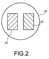
- Fig. 2 shows an example of complementary division of a stencil mask.
- a mask is normally made from a silicon wafer of an 8-inch diameter.
- the stencil mask 100 comprises a first complementary mask 101 and a second complementary mask 102.
- the first complementary mask 101 is used to expose resist to a first complementary pattern formed in the first complementary mask 101.
- a remaining second complementary pattern formed in the second complementary mask 102 is exposed to the resist.
- a plurality of subfield patterns 350 are formed in the first complementary mask 101 and the second complementary mask 102.
- the shot cycle in Fig. 1 indicates a cycle for completing a predetermined pattern 320 in one subfield.
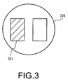
- Fig. 3 shows an example of a membrane mask.
- two pattern portions 201 are formed in the membrane mask 200.
- the membrane mask 200 does not need complementary division. It is thus sufficient to use either of the two pattern portions 201.
- the another of the pattern portions 201 may be used for another chip pattern.
- same patterns may be formed on both of the two pattern portions 201. In this case, a die-to-die inspection can be easily performed at the mask defect inspection process.
- a plurality of subfield patterns 350 are formed in the pattern portion 201.
- the shot cycle in Fig. 1 indicates a cycle for completing a predetermined pattern 320 in one subfield.
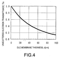
- Fig. 4 shows an example of the relationship between the unscattered electron transmittance and the membrane thickness.
- Fig. 4 shows the case where DLC is used for membrane material.
- the unscattered electron transmittance Tm depends on the membrane thickness. It can be seen that the membrane thickness must be reduced in order to decrease the unscattered electron transmittance Tm and increase the throughput.
- Fig. 5 shows a technique for determining the optimum membrane thickness from a shot cycle.
- the mean free path ⁇ of electrons in the membrane of the membrane mask, the sensitivity S of the resist material, the current density J of electron beam applied by the electron beam exposure apparatus, and the settling time ts of electron beam applied by the electron beam exposure apparatus are used to determine the membrane thickness d so that the shot cycle time tcm that the electron beam exposure apparatus spends in exposing the resist material to form a predetermined pattern using the membrane mask has an operation time comparable to or less than the shot cycle time tcs that the electron beam exposure apparatus spends in exposing the resist material to form the predetermined pattern using the complementary masks.
- the current density J is defined as a current density of the electron beam on a wafer in the case where stencil mask is used (e.g. membrane is not used).
- the beam current density decreases by the amount associated with the transmittance Tm of unscattered electrons.
- tcs ⁇ tcm is satisfied.
- the mean free path ⁇ can be determined experimentally by measuring the transmittance of unscattered electrons. Therefore, the following relation is obtained from Equations 6 and 7: exp ( - d / ⁇ ) ⁇ S / ( J ⁇ ts + 2 S )
- Fig. 6 shows an example of an apparatus for measuring the unscattered electron transmittance.
- the unscattered electron transmittance is measured by EADAM (Energy and Angular Distribution Analysis for Membranes) technique.
- EADAM Electronicgy and Angular Distribution Analysis for Membranes
- Fig. 6 first, without the membrane mask 200, an aperture 410 is vertically exposed to electron beam 401 of 100 keV collimated to 1 nm.
- transmitted electron detection angle aperture diameter
- the electron beam transmitted through the aperture 410 is analyzed by an energy analyzer 420 and separated according to the energy loss, and the signal intensity is measured by a detector 430. Subsequently, with the membrane mask 200 being installed, the same operation is performed.
- Fig. 7 shows the relationship between the detector signal intensity and the energy loss.
- Fig. 7A shows an example result measured without the membrane mask 200.
- the center (100 keV) peak (maximum) value of the detector signal intensity is assumed as unity.
- Fig. 7B shows an example result measured with the membrane mask 200 being installed.
- the peak value of the detector signal intensity for unscattered electrons without energy loss due to inelastic scattering is represented by a value relative to the peak value without the membrane mask 200.
- Fig. 7B shows the peak value of the detector signal intensity of about 41%. That is, the membrane thickness d of the membrane mask 200 used here provides an unscattered electron transmittance Tm of 41%. Substituting these values of the membrane thickness d and the unscattered electron transmittance Tm into Equation 7 described above, the mean free path ⁇ for the membrane material can be determined experimentally.
- Fig. 8 illustrates exposure accuracy for exposure with complementary stencil masks and for exposure with a membrane mask.
- a pattern exposed with the first complementary mask may be misaligned with a pattern exposed with the second complementary mask to result in breaking of circuit. That is, dividing the exposure into two iterations is prone to misalignment which may depend on the accuracy and stability of the exposure system.
- misalignment can be dispensed with because only one iteration of exposure is required.
- a pattern exposed with the first complementary mask may partially overlap with a pattern exposed with the second complementary mask to swell the line width, thereby being connected with the adjacent wiring to cause short circuit.
- the membrane mask is used for exposure, such overlapping pattern can be dispensed with because only one iteration of exposure is required.
- the complementary stencil masks when used for exposure, there is a gap between a pattern exposed with the first complementary mask and a pattern exposed with the second complementary mask. Thereby, a pattern exposed with the first complementary mask disconnects with a pattern exposed with the second complementary mask.
- the resist sensitivity is 5 ⁇ C/cm 2
- the beam current density is 160 mA/cm 2
- the beam settling time is 25 ⁇ s
- the mean free path is 50 nm.
- the optimum membrane thickness is 55 nm. This film thickness provides throughput comparable to the stencil mask. Below this film thickness, the membrane mask has higher throughput.
- the transmittance Tm of the membrane mask that maximizes its mechanical strength is determined from the parameters of the exposure apparatus (beam current density J and beam settling time ts) and the process parameter (resist sensitivity S) and the electron scattering parameter (mean free path ⁇ ) depending on the membrane material.
- the technique for optimizing the membrane thickness d to give this membrane transmittance Tm has been described.
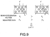
- Fig. 9 illustrates the relationship between the mean free path and the beam acceleration voltage.
- Equation 9 As shown in Fig. 9, as the beam acceleration voltage V increases, the mean free path ⁇ also increases. That is, the mean free path ⁇ is proportional to the beam acceleration voltage V. Therefore, when a mean free path at a certain acceleration voltage is known, an optimum membrane thickness at an arbitrary acceleration voltage can be determined by using Equation 9.
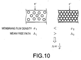
- Fig. 10 illustrates the relationship between the mean free path and the film density of membrane.
- Figs. 11 through 14 show the examples of complementary division of device patterns.
- Fig. 11 shows patterns formed in an active area of a memory cell part of SRAM (static random access memory). As shown in the figure, many doughnut-shape patterns are formed. Each of these patterns are divided and assigned to either of two masks. In the figure, the hatched parts 111 and the dotted parts 112 are divided and assigned to separate mask, respectively.
- Fig. 12 shows patterns formed in a gate layer of a logic device.
- the hatched patterns 111 and the dotted patterns 112 are assigned to separate mask, respectively.
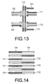
- Fig. 13 shows patterns formed in a peripheral circuit of DRAM (dynamic random access memory).
- DRAM dynamic random access memory
- the doughnut-shape patterns are included.
- the hatched parts 111 and the dotted parts 112 are assigned to separate mask, respectively.
- Fig. 14 shows patterns formed in a memory cell part of DRAM.
- elongated line-and-space patterns are formed.
- the hatched parts 111 and the dotted parts 112 are assigned to separate mask, respectively, in order to prevent the sticking of the patterns.
- the membrane mask having the optimized membrane thickness is balanced from the viewpoint of throughput and mechanical strength.
- the optimum membrane thickness can be determined using the values of beam acceleration voltage, beam current density, and beam settling time of the exposure apparatus, resist sensitivity, and mean free path and density of the membrane. In this way, the parameters of the exposure apparatus and the like can be used to determine the transmittance of the membrane mask that maximizes its mechanical strength from the viewpoint of throughput.
- the membrane thickness that gives this membrane transmittance is the optimum thickness.
- the transmittance of the membrane can be decreased (i.e., the membrane thickness can be increased) by an amount corresponding to one iteration of the above-described settling time. That is, the transmittance does not need to be 50% or more.
- the membrane thickness is determined from the viewpoint of throughput comparable to that of the stencil mask. Unnecessary thinning of membrane may increase performance, but decreases mechanical strength by that amount. This decreases mask yield and increases cost, thus compromising the advantage over the stencil mask.
- Equation 2 there is a good balance when the beam settling time is equal to the resist exposure time. Even if the membrane is thinned and the resist exposure time is further reduced, the effect of throughput improvement gradually decreases.
- DLC is mentioned as membrane material.
- the membrane may be made of various materials such as amorphous carbon, diamond, amorphous silicon, SiN x , SiC x , Si, and SiO 2 , in addition to DLC.
Landscapes
- Physics & Mathematics (AREA)
- General Physics & Mathematics (AREA)
- Electron Beam Exposure (AREA)
- Preparing Plates And Mask In Photomechanical Process (AREA)
Applications Claiming Priority (1)
| Application Number | Priority Date | Filing Date | Title |
|---|---|---|---|
| JP2004212447A JP2006032813A (ja) | 2004-07-21 | 2004-07-21 | メンブレンマスクの製造方法 |
Publications (1)
| Publication Number | Publication Date |
|---|---|
| EP1619551A2 true EP1619551A2 (de) | 2006-01-25 |
Family
ID=35134844
Family Applications (1)
| Application Number | Title | Priority Date | Filing Date |
|---|---|---|---|
| EP05002943A Withdrawn EP1619551A2 (de) | 2004-07-21 | 2005-02-11 | Methode zur Herstellung einer Membranmaske, Methode zur Herstellung eines Halbleiterbauelements und Membranmaske |
Country Status (4)
| Country | Link |
|---|---|
| US (1) | US20060019175A1 (de) |
| EP (1) | EP1619551A2 (de) |
| JP (1) | JP2006032813A (de) |
| TW (1) | TW200604727A (de) |
Families Citing this family (1)
| Publication number | Priority date | Publication date | Assignee | Title |
|---|---|---|---|---|
| JP5611581B2 (ja) * | 2009-12-21 | 2014-10-22 | Hoya株式会社 | マスクブランク及びその製造方法、並びに、転写マスク及びその製造方法 |
Family Cites Families (4)
| Publication number | Priority date | Publication date | Assignee | Title |
|---|---|---|---|---|
| US5876883A (en) * | 1995-12-27 | 1999-03-02 | Vlsi Technology, Inc. | Method forming focus/exposure matrix on a wafer using overlapped exposures |
| JP3706527B2 (ja) * | 1999-06-30 | 2005-10-12 | Hoya株式会社 | 電子線描画用マスクブランクス、電子線描画用マスクおよび電子線描画用マスクの製造方法 |
| JP4746753B2 (ja) * | 2001-03-05 | 2011-08-10 | ルネサスエレクトロニクス株式会社 | 荷電粒子線露光用マスクの形成方法および荷電粒子線用マスクを形成するためのパターンデータの処理プログラム |
| JP2003092250A (ja) * | 2001-09-18 | 2003-03-28 | Hitachi Ltd | 半導体装置及びその製造方法 |
-
2004
- 2004-07-21 JP JP2004212447A patent/JP2006032813A/ja active Pending
-
2005
- 2005-02-11 US US11/055,633 patent/US20060019175A1/en not_active Abandoned
- 2005-02-11 EP EP05002943A patent/EP1619551A2/de not_active Withdrawn
- 2005-02-14 TW TW094104274A patent/TW200604727A/zh unknown
Also Published As
| Publication number | Publication date |
|---|---|
| JP2006032813A (ja) | 2006-02-02 |
| TW200604727A (en) | 2006-02-01 |
| US20060019175A1 (en) | 2006-01-26 |
Similar Documents
| Publication | Publication Date | Title |
|---|---|---|
| US7144178B2 (en) | Mask, method of producing mask, and method of producing semiconductor device | |
| US6043496A (en) | Method of linewidth monitoring for nanolithography | |
| US6597001B1 (en) | Method of electron-beam exposure and mask and electron-beam exposure system used therein | |
| JP2857384B2 (ja) | リソグラフィプロセスを含むデバイス製作法 | |
| US5808312A (en) | System and process for inspecting and repairing an original | |
| US20030132382A1 (en) | System and method for inspecting a mask | |
| JP4603305B2 (ja) | 露光方法、パターン寸法調整方法及び焦点ぼかし量取得方法 | |
| JP2702183B2 (ja) | 半導体製造装置 | |
| US6635402B2 (en) | Devices for measuring and adjusting illumination uniformity obtained from a charged-particle illumination-optical system | |
| US6603120B2 (en) | Test method of mask for electron-beam exposure and method of electron-beam exposure | |
| US6861187B2 (en) | Methods and devices for evaluating imaging characteristics of a charged-particle-beam microlithography system | |
| US20010028037A1 (en) | Hollow-beam aperture for charged-particle-beam optical systems and microlithography apparatus, andbeam-adjustment methods employing same | |
| EP1619551A2 (de) | Methode zur Herstellung einer Membranmaske, Methode zur Herstellung eines Halbleiterbauelements und Membranmaske | |
| JP4690795B2 (ja) | 半導体装置の製造方法 | |
| US11815473B2 (en) | Methods of inspecting samples with multiple beams of charged particles | |
| JP2004095925A (ja) | アライメント方法、アライメント基板、アライメント基板の製造方法、露光方法、露光装置およびマスクの製造方法 | |
| JP2001244165A (ja) | 近接効果補正方法、レチクル及びデバイス製造方法 | |
| Lin et al. | Characteristics performance of production-worthy multiple e-beam maskless lithography | |
| US6627906B2 (en) | Control of exposure in charged-particle-beam microlithography based on beam-transmissivity of the reticle | |
| JP2021162690A (ja) | 検査装置 | |
| JP2003347197A (ja) | マスク検査方法、マスク作成方法およびマスク | |
| US6204511B1 (en) | Electron beam image picturing method and image picturing device | |
| JP2001237175A (ja) | 近接効果補正方法、レチクル及びデバイス製造方法 | |
| Kurokawa et al. | EB resolution capability with CP exposure | |
| JP2007019247A (ja) | 電子ビーム装置およびデバイス製造方法 |
Legal Events
| Date | Code | Title | Description |
|---|---|---|---|
| PUAI | Public reference made under article 153(3) epc to a published international application that has entered the european phase |
Free format text: ORIGINAL CODE: 0009012 |
|
| AK | Designated contracting states |
Kind code of ref document: A2 Designated state(s): AT BE BG CH CY CZ DE DK EE ES FI FR GB GR HU IE IS IT LI LT LU MC NL PL PT RO SE SI SK TR |
|
| AX | Request for extension of the european patent |
Extension state: AL BA HR LV MK YU |
|
| STAA | Information on the status of an ep patent application or granted ep patent |
Free format text: STATUS: THE APPLICATION HAS BEEN WITHDRAWN |
|
| 18W | Application withdrawn |
Effective date: 20051216 |