EP1619718A1 - Dispositif electronique et sa methode de fabrication - Google Patents
Dispositif electronique et sa methode de fabrication Download PDFInfo
- Publication number
- EP1619718A1 EP1619718A1 EP04726313A EP04726313A EP1619718A1 EP 1619718 A1 EP1619718 A1 EP 1619718A1 EP 04726313 A EP04726313 A EP 04726313A EP 04726313 A EP04726313 A EP 04726313A EP 1619718 A1 EP1619718 A1 EP 1619718A1
- Authority
- EP
- European Patent Office
- Prior art keywords
- film
- nitrogen
- dielectric constant
- insulating film
- low dielectric
- Prior art date
- Legal status (The legal status is an assumption and is not a legal conclusion. Google has not performed a legal analysis and makes no representation as to the accuracy of the status listed.)
- Withdrawn
Links
Images



Classifications
-
- H—ELECTRICITY
- H10—SEMICONDUCTOR DEVICES; ELECTRIC SOLID-STATE DEVICES NOT OTHERWISE PROVIDED FOR
- H10W—GENERIC PACKAGES, INTERCONNECTIONS, CONNECTORS OR OTHER CONSTRUCTIONAL DETAILS OF DEVICES COVERED BY CLASS H10
- H10W20/00—Interconnections in chips, wafers or substrates
- H10W20/01—Manufacture or treatment
- H10W20/071—Manufacture or treatment of dielectric parts thereof
-
- H—ELECTRICITY
- H10—SEMICONDUCTOR DEVICES; ELECTRIC SOLID-STATE DEVICES NOT OTHERWISE PROVIDED FOR
- H10W—GENERIC PACKAGES, INTERCONNECTIONS, CONNECTORS OR OTHER CONSTRUCTIONAL DETAILS OF DEVICES COVERED BY CLASS H10
- H10W20/00—Interconnections in chips, wafers or substrates
- H10W20/01—Manufacture or treatment
- H10W20/071—Manufacture or treatment of dielectric parts thereof
- H10W20/074—Manufacture or treatment of dielectric parts thereof of dielectric parts comprising thin functional dielectric layers, e.g. dielectric etch-stop, barrier, capping or liner layers
-
- H—ELECTRICITY
- H10—SEMICONDUCTOR DEVICES; ELECTRIC SOLID-STATE DEVICES NOT OTHERWISE PROVIDED FOR
- H10W—GENERIC PACKAGES, INTERCONNECTIONS, CONNECTORS OR OTHER CONSTRUCTIONAL DETAILS OF DEVICES COVERED BY CLASS H10
- H10W20/00—Interconnections in chips, wafers or substrates
- H10W20/01—Manufacture or treatment
- H10W20/071—Manufacture or treatment of dielectric parts thereof
- H10W20/081—Manufacture or treatment of dielectric parts thereof by forming openings in the dielectric parts
-
- H—ELECTRICITY
- H10—SEMICONDUCTOR DEVICES; ELECTRIC SOLID-STATE DEVICES NOT OTHERWISE PROVIDED FOR
- H10W—GENERIC PACKAGES, INTERCONNECTIONS, CONNECTORS OR OTHER CONSTRUCTIONAL DETAILS OF DEVICES COVERED BY CLASS H10
- H10W20/00—Interconnections in chips, wafers or substrates
- H10W20/01—Manufacture or treatment
- H10W20/071—Manufacture or treatment of dielectric parts thereof
- H10W20/081—Manufacture or treatment of dielectric parts thereof by forming openings in the dielectric parts
- H10W20/084—Manufacture or treatment of dielectric parts thereof by forming openings in the dielectric parts for dual-damascene structures
- H10W20/085—Manufacture or treatment of dielectric parts thereof by forming openings in the dielectric parts for dual-damascene structures involving intermediate temporary filling with material
-
- H—ELECTRICITY
- H10—SEMICONDUCTOR DEVICES; ELECTRIC SOLID-STATE DEVICES NOT OTHERWISE PROVIDED FOR
- H10P—GENERIC PROCESSES OR APPARATUS FOR THE MANUFACTURE OR TREATMENT OF DEVICES COVERED BY CLASS H10
- H10P14/00—Formation of materials, e.g. in the shape of layers or pillars
- H10P14/60—Formation of materials, e.g. in the shape of layers or pillars of insulating materials
- H10P14/63—Formation of materials, e.g. in the shape of layers or pillars of insulating materials characterised by the formation processes
- H10P14/6326—Deposition processes
- H10P14/6328—Deposition from the gas or vapour phase
- H10P14/6334—Deposition from the gas or vapour phase using decomposition or reaction of gaseous or vapour phase compounds, i.e. chemical vapour deposition
- H10P14/6336—Deposition from the gas or vapour phase using decomposition or reaction of gaseous or vapour phase compounds, i.e. chemical vapour deposition in the presence of a plasma [PECVD]
-
- H—ELECTRICITY
- H10—SEMICONDUCTOR DEVICES; ELECTRIC SOLID-STATE DEVICES NOT OTHERWISE PROVIDED FOR
- H10P—GENERIC PROCESSES OR APPARATUS FOR THE MANUFACTURE OR TREATMENT OF DEVICES COVERED BY CLASS H10
- H10P14/00—Formation of materials, e.g. in the shape of layers or pillars
- H10P14/60—Formation of materials, e.g. in the shape of layers or pillars of insulating materials
- H10P14/66—Formation of materials, e.g. in the shape of layers or pillars of insulating materials characterised by the type of materials
- H10P14/665—Porous materials
-
- H—ELECTRICITY
- H10—SEMICONDUCTOR DEVICES; ELECTRIC SOLID-STATE DEVICES NOT OTHERWISE PROVIDED FOR
- H10P—GENERIC PROCESSES OR APPARATUS FOR THE MANUFACTURE OR TREATMENT OF DEVICES COVERED BY CLASS H10
- H10P14/00—Formation of materials, e.g. in the shape of layers or pillars
- H10P14/60—Formation of materials, e.g. in the shape of layers or pillars of insulating materials
- H10P14/69—Inorganic materials
- H10P14/6903—Inorganic materials containing silicon
- H10P14/6905—Inorganic materials containing silicon being a silicon carbide or silicon carbonitride and not containing oxygen, e.g. SiC or SiC:H
-
- H—ELECTRICITY
- H10—SEMICONDUCTOR DEVICES; ELECTRIC SOLID-STATE DEVICES NOT OTHERWISE PROVIDED FOR
- H10P—GENERIC PROCESSES OR APPARATUS FOR THE MANUFACTURE OR TREATMENT OF DEVICES COVERED BY CLASS H10
- H10P14/00—Formation of materials, e.g. in the shape of layers or pillars
- H10P14/60—Formation of materials, e.g. in the shape of layers or pillars of insulating materials
- H10P14/69—Inorganic materials
- H10P14/692—Inorganic materials composed of oxides, glassy oxides or oxide-based glasses
- H10P14/6921—Inorganic materials composed of oxides, glassy oxides or oxide-based glasses containing silicon
- H10P14/69215—Inorganic materials composed of oxides, glassy oxides or oxide-based glasses containing silicon the material being a silicon oxide, e.g. SiO2
-
- H—ELECTRICITY
- H10—SEMICONDUCTOR DEVICES; ELECTRIC SOLID-STATE DEVICES NOT OTHERWISE PROVIDED FOR
- H10P—GENERIC PROCESSES OR APPARATUS FOR THE MANUFACTURE OR TREATMENT OF DEVICES COVERED BY CLASS H10
- H10P14/00—Formation of materials, e.g. in the shape of layers or pillars
- H10P14/60—Formation of materials, e.g. in the shape of layers or pillars of insulating materials
- H10P14/69—Inorganic materials
- H10P14/692—Inorganic materials composed of oxides, glassy oxides or oxide-based glasses
- H10P14/6921—Inorganic materials composed of oxides, glassy oxides or oxide-based glasses containing silicon
- H10P14/6922—Inorganic materials composed of oxides, glassy oxides or oxide-based glasses containing silicon the material containing Si, O and at least one of H, N, C, F or other non-metal elements, e.g. SiOC, SiOC:H or SiONC
-
- H—ELECTRICITY
- H10—SEMICONDUCTOR DEVICES; ELECTRIC SOLID-STATE DEVICES NOT OTHERWISE PROVIDED FOR
- H10P—GENERIC PROCESSES OR APPARATUS FOR THE MANUFACTURE OR TREATMENT OF DEVICES COVERED BY CLASS H10
- H10P14/00—Formation of materials, e.g. in the shape of layers or pillars
- H10P14/60—Formation of materials, e.g. in the shape of layers or pillars of insulating materials
- H10P14/69—Inorganic materials
- H10P14/692—Inorganic materials composed of oxides, glassy oxides or oxide-based glasses
- H10P14/6921—Inorganic materials composed of oxides, glassy oxides or oxide-based glasses containing silicon
- H10P14/6922—Inorganic materials composed of oxides, glassy oxides or oxide-based glasses containing silicon the material containing Si, O and at least one of H, N, C, F or other non-metal elements, e.g. SiOC, SiOC:H or SiONC
- H10P14/6927—Inorganic materials composed of oxides, glassy oxides or oxide-based glasses containing silicon the material containing Si, O and at least one of H, N, C, F or other non-metal elements, e.g. SiOC, SiOC:H or SiONC the material being a silicon oxynitride, e.g. SiON or SiON:H
-
- H—ELECTRICITY
- H10—SEMICONDUCTOR DEVICES; ELECTRIC SOLID-STATE DEVICES NOT OTHERWISE PROVIDED FOR
- H10P—GENERIC PROCESSES OR APPARATUS FOR THE MANUFACTURE OR TREATMENT OF DEVICES COVERED BY CLASS H10
- H10P76/00—Manufacture or treatment of masks on semiconductor bodies, e.g. by lithography or photolithography
- H10P76/20—Manufacture or treatment of masks on semiconductor bodies, e.g. by lithography or photolithography of masks comprising organic materials
- H10P76/204—Manufacture or treatment of masks on semiconductor bodies, e.g. by lithography or photolithography of masks comprising organic materials of organic photoresist masks
- H10P76/2041—Photolithographic processes
Definitions
- the present invention relates to electronic devices and methods for fabricating the same, and more particularly relates to techniques for forming interconnects.
- a film i.e., a low dielectric constant film
- a film made of material whose dielectric constant is lower than that of a silicon oxide film.
- the examples of the low dielectric constant film include a carbon-containing silicon oxide film and a porous film, for example.
- Carbon-containing silicon oxide films contain carbon in the form of a bulky alkyl or phenyl group.
- the density (which is from about 1.0 to about 1.3 g/cm 3 ) of a carbon-containing silicon oxide film is thus lower than the density (which is about 2.3 g/cm 3 ) of a silicon oxide film, and the relative dielectric constant (which is from about 2.0 to about 3.0) of the carbon-containing silicon oxide film is also lower than the relative dielectric constant (which is from about 3.9 to about 4.3) of the silicon oxide film.
- the film density of a low dielectric constant film is lower than that of a conventional insulating film, e.g., a silicon oxide film, provided between interconnects
- the low dielectric constant film when exposed to the air, is likely to absorb nitrogen or the like present in the air. Consequently, when a photolithography process for forming a trench pattern for upper-level metal interconnects is performed on the carbon-containing silicon oxide film with a via hole formed therein, for example, the following problem occurs.
- the photoresist applied cannot be developed sufficiently where it is located near the via hole, which causes the unnecessary photoresist around the via hole to remain.
- the desired trench pattern thus cannot be formed. This problem occurs for the following reasons.
- a non-patent related document 1 (See pp. 39-41 in "Proceedings of the 2002 International Interconnect Technology Conference" by M. Fayolle et al.) disclosed an interconnection structure for preventing resist poisoning and a method for fabricating the interconnection structure.
- FIG. 7 is a cross sectional view illustrating the interconnection structure in a conventional electronic device, disclosed in the non-patent related document 1 .
- lower-level metal interconnects 2 are formed in a first insulating film 1 formed on a silicon substrate (not shown).
- Each lower-level metal interconnect 2 is formed of a barrier metal film 2a and a copper film 2b , and the first insulating film 1 is formed of a silicon oxide film.
- a second insulating film 3 made of a silicon carbide film is formed on the lower-level metal interconnects 2 and the first insulating film 1 .
- a third insulating film 4 made of a carbon-containing silicon oxide film is formed.
- a fourth insulating film 5 made of a silicon carbide film is formed.
- a fifth insulating film 6 made of a carbon-containing silicon oxide film is formed on the fourth insulating film 5 .
- a via hole 7, which reaches at least one of the lower-level metal interconnects 2 is formed in the second and third insulating films 3 and 4 , while a trench for wiring 8 , which reaches the via hole 7 , is formed in the fourth and fifth insulating films 5 and 6 .
- a barrier metal film 9 and a copper film 10 are formed in sequence to form a via plug 11 and upper-level metal interconnects 12 .
- the via plug 11 connects the lower-level metal interconnects 2 and the upper-level metal interconnects 12 .
- FIGS. 8(a) through 8(f) are cross sectional views indicating process steps of a method for fabricating the conventional electronic device disclosed in the non-patent related document 1, that is, a method for fabricating the electronic device shown in FIG. 7.
- a first insulating film 1 is formed on a silicon substrate (not shown), after which lower-level metal interconnects 2 , formed of a barrier metal film 2a and a copper film 2b , are buried in the first insulating film 1 .
- a second insulating film 3 made of a silicon carbide film, a third insulating film 4 made of a carbon-containing silicon oxide film, a fourth insulating film 5 made of a silicon carbide film, a fifth insulating film 6 made of a carbon-containing silicon oxide film, and a sixth insulating film 13 made of a silicon carbide film are deposited in sequence over the first insulating film 1 and the lower-level metal interconnects 2 .
- a photoresist is applied onto the sixth insulating film 13 and a photolithography process is performed on the photoresist, thereby forming a resist film (not shown) having a hole pattern.
- the sixth insulating film 13 and the fifth insulating film 6 are sequentially dry-etched, and then the photoresist is removed by ashing.
- a hole 14 which corresponds to a via hole 7 (see FIG. 8(e) ), is formed in the sixth insulating film 13 and the fifth insulating film 6, as shown in FIG. 8(c).
- a photoresist is applied onto the sixth insulating film 13 and a photolithography process is performed on the photoresist, thereby forming a resist film 15 having a desired trench pattern. More specifically, the resist film 15 , having openings 15a that correspond to a trench for wiring 8 (see FIG. 8(e) ), is formed.
- the sixth insulating film 13 , the fifth insulating film 6 , the fourth insulating film 5 , and the third insulating film 4 are dry-etched in sequence with the resist film 15 having the trench pattern and the sixth and fifth insulating films 13 and 6 having the hole pattern used as masks.
- the via hole 7 is formed in the third insulating film 4, while the trench 8 is formed in the fourth and fifth insulating films 5 and 6 .
- the resist film 15 is removed and a cleaning process is performed.
- part (i.e., the via hole 7 formation region) of the second insulating film 3 , part (i.e., the trench 8 formation region) of the fourth insulating film 5 , and the sixth insulating film 13 , each of which is made of a silicon carbide film, are removed at the same time by performing an etchback process on the entire surface of the substrate.
- the desired via hole 7 and the desired trench 8 are formed.
- a barrier metal film 9 and a copper film 10 are deposited in this order on the fifth insulating film 6 so that the via hole 7 and the trench 8 are filled completely. Thereafter, the barrier metal film 9 and the copper film 10 are removed by a CMP (chemical mechanical polishing) process where they are located externally of the trench 8.
- CMP chemical mechanical polishing
- the fact that the nitrogen-non-containing silicon carbide films, which are poorer in film quality than silicon carbon nitride films, are used instead of using silicon carbon nitride films for the purpose of preventing resist poisoning causes a problem in that the amount of leakage current is increased.
- the film stability of the silicon carbide films is poor, which produces another problem in that the film quality varies with passage of time if the films are left standing after deposited.
- a first inventive electronic device includes: a low dielectric constant film having a hole, a nitrogen-non-containing insulating film formed under the low dielectric constant film, and a nitrogen-containing insulating film formed under the nitrogen-non-containing insulating film.
- the nitrogen-non-containing insulating film is interposed between the low dielectric constant film, serving as an insulating film between interconnects, and the underlying nitrogen-containing insulating film.
- the low dielectric constant film and the nitrogen-containing insulating film are not in direct contact with each other, which suppresses the nitrogen from entering the low dielectric constant film. Therefore, when a chemically amplified resist is applied onto the low dielectric constant film with the hole formed therein, diffusion of an amine or the like from the low dielectric constant film through the hole into the resist, that is, a resist poisoning phenomenon, is prevented.
- the nitrogen-containing insulating film e.g., a silicon carbon nitride film
- the nitrogen-containing insulating film with excellent film quality is formed under the low dielectric constant film, it is possible to prevent leakage current increase or film quality change over time.
- the nitrogen-non-containing insulating film is deposited by, e.g., a plasma CVD (chemical vapor deposition) process, the film quality of the underlying nitrogen-containing insulating film is stabilized, such that nitrogen contained in the nitrogen-containing insulating film is not likely to be liberated. It is thus possible to more reliably suppress the nitrogen from entering the low dielectric constant film.
- a plasma CVD chemical vapor deposition
- nitrogen-non-containing insulating film as used herein means an insulating film in which nitrogen is contained at a concentration less than 1 ⁇ 10 19 atoms/cm 3 .
- the hole preferably passes through the nitrogen-non-containing insulating film and the nitrogen-containing insulating film
- the electronic device preferably further includes a lower-level interconnect which is located under the hole and connected with the hole, and the upper surface of the lower-level interconnect, except for a region in which the lower-level interconnect is connected with the hole, is preferably covered with the nitrogen-containing insulating film.
- the lower surface of the low dielectric constant film is preferably in contact with the upper surface of the nitrogen-non-containing insulating film.
- a second inventive electronic device includes: a low dielectric constant film having a hole, a nitrogen-non-containing insulating film formed over the low dielectric constant film, and a nitrogen-containing insulating film formed over the nitrogen-non-containing insulating film.
- the nitrogen-non-containing insulating film is interposed between the low dielectric constant film, serving as an insulating film between interconnects, and the nitrogen-containing insulating film provided over the low dielectric constant film.
- the low dielectric constant film and the nitrogen-containing insulating film are not in direct contact with each other, which suppresses the nitrogen from entering the low dielectric constant film. Therefore, when a chemically amplified resist is applied over the low dielectric constant film with the hole formed therein, diffusion of an amine or the like from the low dielectric constant film through the hole into the resist, that is, a resist poisoning phenomenon, is prevented.
- the nitrogen-containing insulating film e.g., a silicon carbon nitride film
- the nitrogen-containing insulating film with excellent film quality is formed over the low dielectric constant film, it is possible to prevent leakage current increase or film quality change over time.
- the nitrogen-containing insulating film is formed over the low dielectric constant film with the nitrogen-non-containing insulating film interposed therebetween, so that after the low dielectric constant film is formed, the low dielectric constant film is not directly exposed to an atmosphere (such as plasma) that contains nitrogen. It is therefore possible to more reliably suppress nitrogen from entering the low dielectric constant film.
- the nitrogen-containing insulating film is preferably an anti-reflection film, and a trench, which is connected with the hole, is preferably formed in the nitrogen-containing insulating film, the nitrogen-non-containing insulating film, and at least an upper portion of the low dielectric constant film.
- the upper surface of the low dielectric constant film is preferably in contact with the lower surface of the nitrogen-non-containing insulating film.
- a third inventive electronic device includes: a low dielectric constant film having a hole, a first nitrogen-non-containing insulating film formed under the low dielectric constant film, and a second nitrogen-non-containing insulating film formed over the low dielectric constant film, wherein the hole passes through the first nitrogen-non-containing insulating film, and a trench, which is connected with the hole, is formed in the second nitrogen-non-containing insulating film and at least an upper portion of the low dielectric constant film.
- the nitrogen-non-containing insulating films are formed over and under the low dielectric constant film serving as an insulating film between interconnects, which reliably suppresses nitrogen from entering the low dielectric constant film. Therefore, after the formation of the hole in the low dielectric constant film, when a chemically amplified resist is applied over the low dielectric constant film in the lithography process for forming the trench which is connected with the hole, diffusion of an amine or the like from the low dielectric constant film through the hole into the resist, that is, a resist poisoning phenomenon, is prevented.
- the lower surface of the low dielectric constant film is preferably in contact with the upper surface of the first nitrogen-non-containing insulating film.
- the upper surface of the low dielectric constant film is preferably in contact with the lower surface of the second nitrogen-non-containing insulating film.
- a fourth inventive electronic device includes: a low dielectric constant film having a hole, and a low density insulating film having a film density of 1.3 g/cm 3 or lower and formed over the low dielectric constant film.
- the low density insulating film is formed over the low dielectric constant film serving as an insulating film between interconnects.
- nitrogen taken into the low dielectric constant film and nitrogen present in the low density insulating film itself are externally released easily through the low density insulating film.
- the density of the low density insulating film is preferably 0.4 g/cm 3 or higher in consideration of the stability of the film.
- the low density insulating film preferably contains nitrogen.
- the low density insulating film has excellent film quality, thereby preventing leakage current increase or film quality change over time.
- the fourth inventive electronic device preferably further includes a nitrogen-containing insulating film formed under the low dielectric constant film.
- the nitrogen-containing insulating film has excellent film quality, so that leakage current increase or film quality change over time is prevented.
- the low dielectric constant film is preferably a carbon-containing silicon oxide film or a porous film.
- a SiOC film may be used as the carbon-containing silicon oxide film.
- a first inventive method for fabricating an electronic device includes: the step of forming a nitrogen-non-containing insulating film and a low dielectric constant film in sequence over a nitrogen-containing insulating film; the step of forming a hole in the low dielectric constant film; the step of applying a chemically amplified resist on the low dielectric constant film with the hole formed therein, and subjecting the chemically amplified resist to exposure and development processes, thereby forming a resist film having an opening in a predetermined region that includes a region in which the hole is formed; and the step of etching the low dielectric constant film with the resist film used as a mask, thereby forming a trench which is connected with the hole.
- the chemically amplified resist is applied on the low dielectric constant film.
- the nitrogen-non-containing insulating film is interposed between the low dielectric constant film and the nitrogen-containing insulating film, such that the low dielectric constant film and the nitrogen-containing insulating film are not in direct contact with each other. This suppresses the nitrogen from entering the low dielectric constant film.
- the chemically amplified resist is applied onto the low dielectric constant film with the hole formed therein, diffusion of an amine or the like through the hole into the resist, that is, a resist poisoning phenomenon, is prevented.
- the nitrogen-containing insulating film e.g., a silicon carbon nitride film
- the nitrogen-containing insulating film with excellent film quality is formed under the low dielectric constant film, it is possible to prevent leakage current increase or film quality change over time.
- the nitrogen-non-containing insulating film is deposited by, e.g., a plasma CVD process, the film quality of the underlying nitrogen-containing insulating film is stabilized, such that the nitrogen contained in the nitrogen-containing insulating film is not likely to be liberated. As a result, it is possible to more reliably suppress the nitrogen from entering the low dielectric constant film.
- the nitrogen-containing insulating film is preferably formed so as to cover a lower-level interconnect.
- the hole-forming step preferably includes the step of forming the hole in the low dielectric constant film and the nitrogen-non-containing insulating film, and the method preferably further includes, after the trench-forming step, the step of removing part of the nitrogen-containing insulating film which is located under the hole.
- etching damage and ashing damage examples include, e.g., oxidation of the surfaces of the interconnects, devices and the like.
- a second inventive method for fabricating an electronic device includes: the step of forming a nitrogen-non-containing insulating film and a nitrogen-containing insulating film in sequence over a low dielectric constant film; the step of forming a hole in the low dielectric constant film with the nitrogen-non-containing insulating film and the nitrogen-containing insulating film formed thereon; the step of applying a chemically amplified resist over the low dielectric constant film with the hole formed therein, and subjecting the chemically amplified resist to exposure and development processes, thereby forming a resist film having an opening in a predetermined region that includes a region in which the hole is formed; and the step of etching the low dielectric constant film with the resist film used as a mask, thereby forming a trench which is connected with the hole.
- the hole is formed in the low dielectric constant film.
- the chemically amplified resist is applied over the low dielectric constant film.
- the nitrogen-non-containing insulating film is interposed between the low dielectric constant film and the nitrogen-containing insulating film, so that the low dielectric constant film and the nitrogen-containing insulating film are not in direct contact with each other. This suppresses the nitrogen from entering the low dielectric constant film.
- the chemically amplified resist is applied over the low dielectric constant film with the hole formed therein, diffusion of an amine or the like through the hole into the resist, that is, a resist poisoning phenomenon, is prevented.
- the nitrogen-containing insulating film e.g., a silicon carbon nitride film
- the nitrogen-containing insulating film with excellent film quality is formed over the low dielectric constant film, it is possible to prevent leakage current increase or film quality change over time.
- the nitrogen-containing insulating film is formed over the low dielectric constant film with the nitrogen-non-containing insulating film interposed therebetween, the low dielectric constant film is not directly exposed to an atmosphere (such as plasma) that contains nitrogen, after the low dielectric constant film is formed. It is thus possible to more reliably suppress nitrogen from entering the low dielectric constant film.
- the nitrogen-containing insulating film preferably functions as an anti-reflection film in the resist-film forming step.
- a third inventive method for fabricating an electronic device includes: the step of forming a low dielectric constant film and a second nitrogen-non-containing insulating film in sequence over a first nitrogen-non-containing insulating film; the step of forming a hole in the low dielectric constant film with the second nitrogen-non-containing insulating film formed thereon; the step of applying a chemically amplified resist over the low dielectric constant film with the hole formed therein, and subjecting the chemically amplified resist to exposure and development processes, thereby forming a resist film having an opening in a predetermined region that includes a region in which the hole is formed; and the step of etching the low dielectric constant film with the resist film used as a mask, thereby forming a trench which is connected with the hole.
- the chemically amplified resist is applied over the low dielectric constant film. It is therefore possible to reliably suppress nitrogen from entering the low dielectric constant film.
- the chemically amplified resist is applied over the low dielectric constant film with the hole formed therein, diffusion of an amine or the like through the hole into the resist, that is, a resist poisoning phenomenon, is prevented.
- the nitrogen-non-containing insulating films are preferably deposited by a CVD process.
- the density (which is about 2.3 g/cm 3 ) of the silicon oxide films is greater than the density of the low dielectric constant film, which is a carbon-containing silicon oxide film, for example.
- the nitrogen-non-containing insulating films formed out of the silicon oxide films function as barrier layers against nitrogen. It is therefore possible to more reliably suppress nitrogen from entering the low dielectric constant film.
- the first, second, and third inventive methods preferably further include, between the hole-forming step and the resist-film forming step, the step of forming a dummy plug in the hole.
- the dummy plug made of, e.g., an organic material, covers the wall surface of the hole which includes the interface(s) between the low dielectric constant film and the nitrogen-non-containing insulating film(s). More specifically, since the interface(s) and a damage layer in the wall surface of the hole are covered by the dummy plug, nitrogen diffusion from the interface(s) or the damage layer into the hole is suppressed, thereby reliably avoiding resist poisoning.
- a fourth inventive method for fabricating an electronic device includes: the step of forming a low density insulating film whose film density is 1.3 g/cm 3 or lower on a low dielectric constant film; the step of forming a hole in the low dielectric constant film with the low density insulating film formed thereon; the step of applying a chemically amplified resist over the low dielectric constant film with the hole formed therein, and subjecting the chemically amplified resist to exposure and development processes, thereby forming a resist film having an opening in a predetermined region that includes a region in which the hole is formed; and the step of etching the low dielectric constant film with the resist film used as a mask, thereby forming a trench which is connected with the hole.
- the hole is formed in the low dielectric constant film.
- the chemically amplified resist is applied over the low dielectric constant film.
- nitrogen taken into the low dielectric constant film and nitrogen present in the low density insulating film itself are externally released easily through the low density insulating film.
- the chemically amplified resist is applied over the low dielectric constant film, the amount of an amine or the like present per unit volume of the resist where the resist is located near the hole is reduced extremely, which results in the prevention of resist poisoning.
- the density of the low density insulating film is preferably 0.4 g/cm 3 or higher in consideration of the stability of the film.
- the fourth inventive method preferably further includes, after the low-density-insulating-film forming step, the step of subjecting the low density insulating film to a heat treatment or applying an energy wave to the low density insulating film.
- the film quality of the low density insulating film is stabilized, while a greater amount of nitrogen is released externally from the low dielectric constant film and the low density insulating film through the low density insulating film.
- the energy wave is an electron beam or ultraviolet radiation, the above-mentioned effect is achieved reliably.
- the low dielectric constant film is preferably a carbon-containing silicon oxide film or a porous film.
- a SiOC film may be used as the carbon-containing silicon oxide film.
- FIG. 1 is a cross sectional view illustrating an interconnection structure in the electronic device in accordance with the first embodiment.
- lower-level metal interconnects 102 are formed in a lower-level insulating film 101 formed on a substrate 100 made of, e.g., silicon.
- Each lower-level metal interconnect 102 is formed of, e.g., a tantalum-nitride/tantalum multilayer film 102a and a copper film 102b .
- a first nitrogen-containing insulating film 103 made of, e.g., a silicon carbon nitride film is formed.
- a first nitrogen-non-containing insulating film 104 made of, e.g., a silicon oxide film is formed.
- a low dielectric constant film 105 made of, e.g., a carbon-containing silicon oxide film is formed.
- a second nitrogen-non-containing insulating film 106 made of, e.g., a silicon oxide film is formed.
- a second nitrogen-containing insulating film 107 made of, e.g., a silicon oxynitride film is formed.
- a via hole 108 which reaches at least one of the lower-level metal interconnects 102 , is formed.
- a trench for wiring 109 which is connected with the via hole 108 , is formed.
- a tantalum-nitride/tantalum multilayer film 110 and a copper film 111 are formed in sequence to form a via plug 112 and upper-level metal interconnects 113 .
- the via plug 112 connects the lower-level metal interconnects 102 with the upper-level metal interconnects 113 .
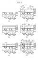
- FIGS. 2(a) through 2(f) are cross sectional views indicating process steps of a method for fabricating the electronic device of the first embodiment, that is, a method for fabricating the electronic device shown in FIG. 1 .
- a lower-level insulating film 101 made of, e.g., a silicon oxide film is formed on a substrate 100 made of, e.g., silicon, after which lower-level metal interconnects 102 , formed of, e.g., a tantalum-nitride/tantalum multilayer film 102a and a copper film 102b , are buried in the lower-level insulating film 101 .
- a resist film (not shown) having a trench pattern for the lower-level metal interconnects is formed on the lower-level insulating film 101 by a photolithography process, and the lower-level insulating film 101 is then dry-etched with the resist film used as a mask, thereby forming a trench for wiring.
- the tantalum-nitride/tantalum multilayer film 102a and the copper film 102b are deposited in this order on the lower-level insulating film 101 so that the trench is filled completely.
- the multilayer film 102a and the copper film 102b are then removed by a CMP process where they are located externally of the trench, thereby forming the lower-level metal interconnects 102 .
- a first nitrogen-containing insulating film 103 made of, e.g., a silicon carbon nitride film is deposited to a thickness of 50 nm on the lower-level insulating film 101 and the lower-level metal interconnects 102 .
- a first nitrogen-non-containing insulating film 104 made of, e.g., a silicon oxide film is deposited to a thickness of 50 nm on the first nitrogen-containing insulating film 103 .
- the silicon oxide film, serving as the first nitrogen-non-containing insulating film 104 is deposited by a plasma CVD process in which TEOS, for example, is used.
- a low dielectric constant film 105 made of, e.g., a carbon-containing silicon oxide film is deposited to a thickness of 450 nm on the first nitrogen-non-containing insulating film 104 .
- a second nitrogen-non-containing insulating film 106 made of, e.g., a silicon oxide film is then deposited to a thickness of 30 nm.
- the silicon oxide film, serving as the second nitrogen-non-containing insulating film 106 is deposited by a plasma CVD process in which TEOS, for example, is used.
- a second nitrogen-containing insulating film 107 made of, e.g., a silicon oxynitride film is deposited to a thickness of 50 nm on the second nitrogen-non-containing insulating film 106 .
- the silicon oxynitride film, serving as the second nitrogen-containing insulating film 107 will act as an anti-reflection film in a later photolithography process.
- the thickness of the silicon oxynitride film serving as the anti-reflection film is preferably from 60 nm to 100 nm in the case of a design rule greater than 0.18 ⁇ m, and preferably from 30 nm to 70 nm in the case of a 0.18 ⁇ m or smaller design rule.
- a photoresist is applied onto the second nitrogen-containing insulating film 107 and a photolithography process is performed on the photoresist, thereby forming a resist film (not shown) having a hole pattern.
- the second nitrogen-containing insulating film 107 , the second nitrogen-non-containing insulating film 106 , the low dielectric constant film 105 and the first nitrogen-non-containing insulating film 104 are dry-etched in sequence, and the photoresist is then removed by ashing. By these steps, a via hole 108 is formed, as shown in FIG. 2(a).
- a dummy plug 114 made of, e.g., an organic material, is formed in the via hole 108.
- the dummy plug 114 is formed in such a manner that the upper surface of the dummy plug 114 is higher than the interface between the low dielectric constant film 105 and the second nitrogen-non-containing insulating film 106 .
- the formation of the dummy plug 114 is not indispensable in this embodiment.
- a photoresist is applied onto the second nitrogen-containing insulating film 107 and then a photolithography (exposure and development) process is performed on the photoresist, thereby forming a resist film 115 having a desired trench pattern. More specifically, the resist film 115 having openings 115a that correspond to a trench for wiring 109 (see FIG. 2(e) ) is formed.
- the regions in which the openings 115a are formed include the region in which the via hole 108 is formed.
- the second nitrogen-containing insulating film 107 , the second nitrogen-non-containing insulating film 106 and (the upper portion of) the low dielectric constant film 105 are sequentially dry-etched with the dummy plug 114 and the resist film 115 having the trench pattern used as masks.
- the trench 109 which is connected with the via hole 108 , is formed, as shown in FIG. 2(e) . It should be noted that after the dry-etching process, the dummy plug 114 and the resist film 115 are removed and a cleaning process is then performed.
- a tantalum-nitride/tantalum multilayer film 110 and a copper film 111 are then deposited in sequence on the second nitrogen-containing insulating film 107 so that the via hole 108 and the trench 109 are filled completely.
- the multilayer film 110 and the copper film 111 are then removed by a CMP process where they are located externally of the trench 109 .
- a via plug 112 is formed in the via hole 108, while upper-level metal interconnects 113 are formed in the trench 109 .
- these films may be completely or partially removed by the above-mentioned etchback process or CMP process.
- the first nitrogen-non-containing insulating film 104 is interposed between the low dielectric constant film (i.e., the carbon-containing silicon oxide film) 105 and the first nitrogen-containing insulating film (i.e., the silicon carbon nitride film) 103 located under the low dielectric constant film 105 . Therefore, resist poisoning is suppressed for the following three reasons, despite the fact that the first nitrogen-containing insulating film 103 is used.
- the effects mentioned above allow resist poisoning to be suppressed, while permitting the formation of the first nitrogen-containing insulating film 103 (e.g., a silicon carbon nitride film) with excellent film quality under the low dielectric constant film 105 . Accordingly, it is possible to prevent leakage current increase or film quality changes with time. Moreover, since the silicon carbon nitride film, serving as the first nitrogen-containing insulating film 103 , does not contain oxygen, the copper films 102b are not oxidized when the first nitrogen-containing insulating film 103 is deposited on the copper films 102b that form the lower-level metal interconnects 102 .
- the silicon carbon nitride film serving as the first nitrogen-containing insulating film 103 .
- the second nitrogen-non-containing insulating film 106 is interposed between the low dielectric constant film (i.e., the carbon-containing silicon oxide film) 105 and the second nitrogen-containing insulating film (i.e., the silicon oxynitride film) 107 provided over the low dielectric constant film 105 .
- the low dielectric constant film i.e., the carbon-containing silicon oxide film
- the second nitrogen-containing insulating film i.e., the silicon oxynitride film
- the effects mentioned above allow resist poisoning to be suppressed, while permitting the formation of the second nitrogen-containing insulating film 107 (e.g., a silicon carbon nitride film) with excellent film quality over the low dielectric constant film 105 . Accordingly, it is possible to prevent leakage current increase or film quality changes with time. Moreover, the silicon oxynitride film having the reflection-preventing effect is used as the second nitrogen-containing insulating film 107 . This eliminates the need for forming a new anti-reflection film, made of, e.g., an organic material, in the lithography processes for forming the via hole 108 and the trench 109 , thereby allowing the number of process steps to be reduced.
- the second nitrogen-containing insulating film 107 e.g., a silicon carbon nitride film
- the first nitrogen-containing insulating film 103 is left under the via hole 108 , that is, on the lower-level metal interconnects 102 , until the formation of the trench 109 is completed. This reduces damage (e.g., oxidation of the surfaces of the lower-level metal interconnects 102 ) to the lower-level metal interconnects 102 , caused by the etching and ashing processes.
- the dummy plug 114 is formed in the via hole 108 prior to the photolithography process for forming the trench 109 . Therefore, the dummy plug 114 covers the wall surface of the via hole 108 , which includes the interfaces between the low dielectric constant film 105 and the first and second nitrogen-non-containing insulating films 104 and 106 . More specifically, since those interfaces and a damage layer in the wall surface of the via hole 108 are covered by the dummy plug 114 , nitrogen diffusion from the interfaces or the damage layer into the via hole 108 is prevented, thereby reliably avoiding resist poisoning. In addition, the presence of the dummy plug 114 in the via hole 108 allows the surface of the resist applied to be planarized, so that the accuracy of the pattern obtained by the photolithography process is increased.
- a silicon oxynitride film having the effect of preventing reflection is used as the second nitrogen-containing insulating film 107 .
- another kind of insulating film that contains nitrogen (more accurately, a film containing nitrogen at a concentration of 1 ⁇ 10 19 atoms/cm 3 or higher) may be used.
- the second nitrogen-containing insulating film 107 can be used as a hard mask in the etching process for forming the via hole 108 or the trench 109 .
- a porous film or a film i.e., an insulating film having a further lower dielectric constant
- a silicon carbon nitride (SiCN) film may be used as the second nitrogen-containing insulating film 107 .
- a silicon carbon nitride film is used as the first nitrogen-containing insulating film 103 .
- another kind of insulating film that contains nitrogen e.g., a silicon nitride film (a SiN film) may be used.
- silicon oxide films are used as the first and second nitrogen-non-containing insulating films 104 and 106 .
- silicon oxide films instead of the silicon oxide films, other kinds of insulating films that contain no nitrogen (more accurately, films that contain nitrogen at a concentration less than 1 ⁇ 10 19 atoms/cm 3 ), e.g., oxygen-added silicon carbide films (SiCO films) or silicon carbide films (SiC films) may be used.
- a SiOC film e.g., may be used as the carbon-containing silicon oxide film serving as the low dielectric constant film 105 .
- the lower surface of the low dielectric constant film 105 is in direct contact with (the upper surface of) the first nitrogen-non-containing insulating film 104 .
- another nitrogen-non-containing insulating film may be provided between the low dielectric constant film 105 and the first nitrogen-non-containing insulating film 104 .
- the upper surface of the low dielectric constant film 105 is in direct contact with (the lower surface of) of the second nitrogen-non-containing insulating film 106
- another nitrogen-non-containing insulating film may be provided between the low dielectric constant film 105 and the second nitrogen-non-containing insulating film 106 .
- the present invention is applied to form the interconnection structure including the lower-level metal interconnects 102 and the upper-level metal interconnects 113 that are connected with each other by the via plug 112 , the present invention is not limited to this. It will be obvious that the present invention is applicable to, for example, formation of a memory cell structure including a transistor (i.e., doped layers thereof) and a capacitor (i.e., a lower electrode thereof) that are connected with each other by a contact plug.
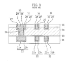
- FIG. 3 is a cross sectional view illustrating the interconnection structure in the electronic device in accordance with the comparative example.
- a second insulating film (a nitrogen-containing insulating film) 23 made of a silicon carbon nitride film is formed on the lower-level metal interconnects 22 and the first insulating film 21 .
- a second insulating film (a nitrogen-containing insulating film) 23 made of a silicon carbon nitride film is formed on the second insulating film 23 .
- a third insulating film (a low dielectric constant film) 24 made of a carbon-containing silicon oxide film is formed on the third insulating film 24 .
- a fourth insulating film 25 made of a silicon oxide film is formed on the third insulating film 24 .
- the fourth insulating film 25 is formed using plasma which is free of contamination with nitrogen.
- a via hole 26 which reaches at least one of the lower-level metal interconnects 22 , is formed.
- a trench for wiring 27 which is connected with the via hole 26 , is formed.
- a tantalum-nitride/tantalum multilayer film 28 and a copper film 29 are formed in sequence to form a via plug 30 and upper-level metal interconnects 31 .
- the via plug 30 connects the lower-level metal interconnects 22 with the upper-level metal interconnects 31.
- FIGS. 4(a) through 4(f) are cross sectional views indicating process steps of a method for fabricating the electronic device according to the comparative example, that is, a method for fabricating the electronic device shown in FIG. 3 .
- a first insulating film 21 is formed on a silicon substrate (not shown), after which lower-level metal interconnects 22, made of a tantalum-nitride/tantalum multilayer film 22a and a copper film 22b, are buried in the first insulating film 21 .
- a second insulating film 23 made of a silicon carbon nitride film is deposited on the first insulating film 21 and the lower-level metal interconnects 22 . Thereafter, the second insulating film 23 is subjected to a plasma treatment so that the film quality of the second insulating film 23 is stabilized. Subsequently, a third insulating film 24 made of a carbon-containing silicon oxide film is deposited on the second insulating film 23 . Then, on the third insulating film 24 , a fourth insulating film 25 made of a silicon oxide film is deposited by a plasma CVD process, after which an organic anti-reflection film 32 is formed on the fourth insulating film 25 . It should be noted that the fourth insulating film 25 is formed using nitrogen-contamination-free plasma, after the underlying third insulating film 24 is subjected to a pretreatment which is free of nitrogen contamination.
- a photoresist is applied onto the organic anti-reflection film 32 and a photolithography process is performed on the photoresist, thereby forming a resist film (not shown) having a hole pattern.
- the organic anti-reflection film 32, the fourth insulating film 25 and the third insulating film 24 are sequentially dry-etched, and the photoresist and the organic anti-reflection film 32 are then removed by ashing.
- a via hole 26 is formed, as shown in FIG. 4(c).
- a lower-level resist film 33 is deposited on the fourth insulating film 25 so that the via hole 26 is filled completely, after which a SOG (spin on glass) film 34 is formed on the lower-level resist film 33.
- a photoresist is applied onto the SOG film 34 and a photolithography process is performed on the photoresist, thereby forming an upper-level resist film 35 having a desired trench pattern. More specifically, the upper-level resist film 35 having openings 35a that correspond to a trench for wiring 27 (see FIG. 4(e)) is formed.
- the SOG film 34 is dry-etched with the upper-level resist film 35 having the trench pattern used as a mask. Subsequently, with the patterned SOG film 34 (having the trench pattern) used as a mask, the lower-level resist film 33, the fourth insulating film 25, and (the upper portion of) the third insulating film 24 are dry-etched in this order. By these steps, as shown in FIG. 4(e), the trench 27, which is connected with the via hole 26, is formed. It should be noted that after the dry-etching process, the upper-level resist film 35, the SOG film 34, and the lower-level resist film 33 are removed and a cleaning process is performed.
- part of the second insulating film 23 which is located under the via hole 26 is removed by performing an etchback process on the entire surface of the substrate. Thereafter, a tantalum-nitride/tantalum multilayer film 28 and a copper film 29 are deposited in this order on the fourth insulating film 25 so that via hole 26 and the trench 27 are filled completely. The multilayer film 28 and the copper film 29 are then removed by a CMP process where they are located externally of the trench 29 . By these steps, as shown in FIG. 4(f), a via plug 30 is formed in the via hole 26, while upper-level metal interconnects 31 are formed in the trench 27 .
- the second insulating film 23 that is, the silicon carbon nitride film, is plasma-treated for stabilization of the film quality, thereby suppressing resist poisoning.
- the third insulating film i.e., the low dielectric constant film
- the fourth insulating film 25 that is, the silicon oxide film
- the third insulating film (i.e., the low dielectric constant film) 24 by using nitrogen-contamination-free plasma, whereby resist poisoning is suppressed.
- the silicon oxide film has no reflection-preventing effect, such that the organic anti-reflection film 32 has to be provided when the pattern for forming the via hole 26 is formed by lithography. Nevertheless, since the coating film thickness of the organic anti-reflection film 32 is large and it is difficult to secure the selective ratio of the organic anti-reflection film 32 with respect to the photoresist, the etching process for forming the via hole 26 becomes difficult.
- the lower-level resist film 33 , the SOG film 34 and the upper-level resist film 35 are used in combination, when the pattern for forming the trench 27 is formed by lithography. This makes it difficult to perform the etching process for forming the trench 27 . In this case, if a dimensional deviation or a misalignment occurs in the lithography process, regeneration of the pattern becomes difficult due to the use of the SOG film 34 . More specifically, unlike a resist film, the SOG film 34 cannot be removed easily by ashing or the like.
- a process, in which a nitrogen-containing insulating film such as a silicon nitride film is formed on the low dielectric constant film and then used as a hard mask in an etching process is effective in terms of achieving a low selective ratio with respect to the photoresist, as well as preventing ashing damage.
- a nitrogen-containing insulating film such as a silicon nitride film is formed on the low dielectric constant film and then used as a hard mask in an etching process
- the comparative example is disadvantageous.
- the relative dielectric constant of the above-mentioned silicon oxide film is as high as about 4.2, which causes the problem of increasing capacitance between the interconnects. Therefore, the comparative example is also unfavorable in terms of lowering of dielectric constant required in insulating films in the future.
- the structure in which the first nitrogen-non-containing insulating film 104 is interposed between the low dielectric constant film 105 and the first nitrogen-containing insulating film 103 located under the low dielectric constant film 105 , and the second nitrogen-non-containing insulating film 106 is interposed between the low dielectric constant film 105 and the second nitrogen-containing insulating film 107 provided over the low dielectric constant film 105 , achieves the outstanding effect of solving all of the above-mentioned problems occurring in the comparative example.
- FIG. 5 is a cross sectional view illustrating an interconnection structure in the electronic device in accordance with the second embodiment.
- lower-level metal interconnects 202 are formed in a lower-level insulating film 201 formed on a substrate 200 made of, e.g., silicon.
- a nitrogen-containing insulating film 203 made of, e.g., a silicon carbon nitride film is formed on the lower-level metal interconnects 202 and the lower-level insulating film 201 .
- a low dielectric constant film 204 made of, e.g., a carbon-containing silicon oxide film is formed on the nitrogen-containing insulating film 203 .
- a low density insulating film (a low density cap film) 205 whose film density is 1.3 g/cm 3 or lower is formed.
- a via hole 206 which reaches at least one of the lower-level metal interconnects 202 , is formed.
- a trench for wiring 207 which is connected with the via hole 206 , is formed.
- a tantalum-nitride/tantalum multilayer film 208 and a copper film 209 are formed in sequence to form a via plug 210 and upper-level metal interconnects 211 .
- FIGS. 6(a) through 6(f) are cross sectional views indicating process steps of a method for fabricating the electronic device according to the second embodiment, that is, a method for fabricating the electronic device shown in FIG. 5 .
- a lower-level insulating film 201 made of, e.g., a silicon oxide film is formed on a substrate 200 made of, e.g., silicon, after which lower-level metal interconnects 202 , made of, e.g., a tantalum-nitride/tantalum multilayer film 202a and a copper film 202b , are buried in the lower-level insulating film 201 .
- a nitrogen-containing insulating film 203 made of, e.g., a silicon carbon nitride film or a silicon nitride film is deposited to a thickness of 50 nm on the lower-level insulating film 201 and the lower-level metal interconnects 202.
- a low dielectric constant film 204 made of, e.g., a carbon-containing silicon oxide film is deposited to a thickness of 450 nm on the nitrogen-containing insulating film 203.
- a low density cap film 205 whose film density is 1.3 g/cm 3 or lower and whose thickness is 50 nm is formed. Thereafter, an organic material, for example, is applied onto the low density cap film 205 to form a first anti-reflection film 212 .
- a photoresist is applied onto the first anti-reflection film 212 and a photolithography process is performed on the photoresist, thereby forming a resist film (not shown) having a hole pattern.
- the first anti-reflection film 212 , the low density cap film 205 and the low dielectric constant film 204 are sequentially dry-etched, and the photoresist and the first anti-reflection film 212 are then removed by ashing.
- a via hole 206 is formed, as shown in FIG. 6(c).
- an organic material for example, is applied onto the low density cap film 205 so that the via hole 206 is filled completely, thereby forming a second anti-reflection film 213 .
- a photoresist is applied onto the second anti-reflection film 213 , and a photolithography (exposure and development) process is performed on the photoresist, thereby forming a resist film 214 having a desired trench pattern. More specifically, the resist film 214 having openings 214a that correspond to a trench for wiring 207 (see FIG. 6(e) ) is formed.
- the regions in which the openings 214a are formed include the region in which the via hole 206 is formed.
- the second anti-reflection film 213, the low density cap film 205, and (the upper portion of) the low dielectric constant film 204 are dry-etched in sequence, thereby forming the trench 207 , which is connected with the via hole 206 , as shown in FIG. 6(e) . It should be noted that after the dry-etching process, the remaining second anti-reflection film 213 and the resist film 214 are removed and a cleaning process is performed.
- part of the nitrogen-containing insulating film 203 formed of the silicon carbon nitride film, which is located under the via hole 206 is removed by performing an etchback process on the entire surface of the substrate.
- a tantalum-nitride/tantalum multilayer film 208 and a copper film 209 are deposited in sequence on the low density cap film 205 so that the via hole 206 and the trench 207 are filled completely.
- the multilayer film 208 and the copper film 209 are then removed by a CMP process where they are located externally of the trench 207.
- a via plug 210 is formed in the via hole 206, while upper-level metal interconnects 211 are formed in the trench 207 . It should be noted that since the low density cap film 205 does not necessarily have to be left finally, this film may be completely or partially removed by the above-mentioned etchback process or CMP process.
- the low density cap film 205 is formed on the low dielectric constant film (i.e., the carbon-containing silicon oxide film) 204 .
- the low dielectric constant film 204 i.e., the carbon-containing silicon oxide film
- nitrogen taken into the low dielectric constant film 204 , nitrogen within the nitrogen-containing insulating film 203 , and nitrogen present in the low density cap film 205 itself are likely to be released externally through the low density cap film 205 .
- the effects mentioned above allow resist poisoning to be suppressed, while permitting the formation of the nitrogen-containing insulating film 203 (e.g., a silicon carbon nitride film) with excellent film quality under the low dielectric constant film 204 . It is thus possible to prevent leakage current increase or film quality changes with time. Moreover, since the silicon carbon nitride film, serving as the nitrogen-containing insulating film 203 , does not contain oxygen, the copper films 202b are not oxidized when the nitrogen-containing insulating film 203 is deposited on the copper films 202b that form the lower-level metal interconnects 202 .
- the nitrogen-containing insulating film 203 e.g., a silicon carbon nitride film
- the nitrogen-containing insulating film 203 is left under the via hole 206 , that is, on the lower-level metal interconnects 202 , until the formation of the trench 207 is completed. This reduces damage (e.g., oxidation of the surfaces of the lower-level metal interconnects 202 ) to the lower-level metal interconnects 202 , caused by the etching and ashing processes.
- the second anti-reflection film 213 is buried in the via hole 206 , before the photolithography process for forming the trench 207 is performed.
- the second anti-reflection film 213 thus covers the wall surface of the via hole 206 .
- a damage layer in the wall surface of the via hole 206 is covered by the second anti-reflection film 213 .
- nitrogen diffusion from the damage layer into the via hole 206 is suppressed, thereby preventing resist poisoning more reliably.
- the kind of insulating film usable as the low density cap film 205 is not limited particularly, so long as the film employed has a film density of 1.3 g/cm 3 or lower.
- a film that has not only a low density but also a low dielectric constant, for example, a porous film is used as the low density cap film 205 , capacitance between the interconnects is reduced.
- a porous film such as a HSQ (hydrogen silsesquioxane) film or a XLK film (whose density is about 0.9 g/cm 3 ) fabricated by Dow Corning, may be used.
- the low density cap film 205 contains nitrogen, the film quality of the low density cap film 205 is improved, so that leakage current increase or film quality changes with time is prevented.
- the low density cap film 205 does not contain carbon. This is because when a carbon-containing film such as a SiOC film is subjected to an ashing process, carbon is eliminated from the film, causing leakage current to flow easily.
- the density of the low density cap film 205 is preferably 0.4 g/cm 3 or higher in consideration of the stability of the film.
- the low density cap film 205 be subjected to, e.g., a heat treatment at about 300 to 400 C°, or an EB (electron beam) cure process or a DUV (deep ultraviolet) cure process. Then, the quality of the low density cap film 205 is stabilized, while a greater amount of nitrogen is released externally through the low density cap film 205 from the nitrogen-containing insulating film 203 , the low dielectric constant film 204 , and the low density cap film 205 . It should be noted that instead of the EB and the DUV, light or an energy wave, which is other than DUV and capable of stabilizing the film quality of the low density cap film 205 , may be applied to the low density cap film 205 .
- a carbon-containing silicon oxide film such as a SiOC film, a Silk film, or a porous film such as a MSQ (methyl silsesquioxane) film, for example, may be used as the low dielectric constant film 204 .
- a carbon-containing silicon oxide film such as a SiOC film, a Silk film, or a porous film such as a MSQ (methyl silsesquioxane) film, for example, may be used as the low dielectric constant film 204 .
- the present invention is applied to form the interconnection structure including the lower-level metal interconnects 202 and the upper-level metal interconnects 211 that are connected with each other by the via plug 210 , the present invention is not limited to this. It will be obvious that the present invention is applicable to, for example, formation of a memory cell structure including a transistor (i.e., doped layers thereof) and a capacitor (i.e., a lower electrode thereof) that are connected with each other by a contact plug.
- a memory cell structure including a transistor (i.e., doped layers thereof) and a capacitor (i.e., a lower electrode thereof) that are connected with each other by a contact plug.
- the present invention relates to electronic devices and methods for fabricating the devices, and when applied to, e.g., formation of a multilevel interconnection structure, the present invention achieves the outstanding effect of preventing resist poisoning in lithography process steps.
Landscapes
- Internal Circuitry In Semiconductor Integrated Circuit Devices (AREA)
Applications Claiming Priority (2)
| Application Number | Priority Date | Filing Date | Title |
|---|---|---|---|
| JP2003104499 | 2003-04-08 | ||
| PCT/JP2004/005044 WO2004090974A1 (fr) | 2003-04-08 | 2004-04-07 | Dispositif electronique et sa methode de fabrication |
Publications (2)
| Publication Number | Publication Date |
|---|---|
| EP1619718A1 true EP1619718A1 (fr) | 2006-01-25 |
| EP1619718A4 EP1619718A4 (fr) | 2009-05-06 |
Family
ID=33156856
Family Applications (1)
| Application Number | Title | Priority Date | Filing Date |
|---|---|---|---|
| EP04726313A Withdrawn EP1619718A4 (fr) | 2003-04-08 | 2004-04-07 | Dispositif electronique et sa methode de fabrication |
Country Status (6)
| Country | Link |
|---|---|
| US (1) | US20060163730A1 (fr) |
| EP (1) | EP1619718A4 (fr) |
| JP (1) | JPWO2004090974A1 (fr) |
| CN (1) | CN1698194A (fr) |
| TW (1) | TW200428586A (fr) |
| WO (1) | WO2004090974A1 (fr) |
Families Citing this family (22)
| Publication number | Priority date | Publication date | Assignee | Title |
|---|---|---|---|---|
| JP4715207B2 (ja) * | 2004-01-13 | 2011-07-06 | 東京エレクトロン株式会社 | 半導体装置の製造方法及び成膜システム |
| US20060183055A1 (en) * | 2005-02-15 | 2006-08-17 | O'neill Mark L | Method for defining a feature on a substrate |
| US7638859B2 (en) * | 2005-06-06 | 2009-12-29 | Taiwan Semiconductor Manufacturing Co., Ltd. | Interconnects with harmonized stress and methods for fabricating the same |
| KR100657166B1 (ko) * | 2005-08-30 | 2006-12-13 | 동부일렉트로닉스 주식회사 | 구리 금속 배선의 형성 방법 |
| JP2007220998A (ja) * | 2006-02-17 | 2007-08-30 | Matsushita Electric Ind Co Ltd | 半導体装置の製造方法 |
| US7488682B2 (en) * | 2006-10-03 | 2009-02-10 | International Business Machines Corporation | High-density 3-dimensional resistors |
| US7884019B2 (en) * | 2007-06-07 | 2011-02-08 | Texas Instruments Incorporated | Poison-free and low ULK damage integration scheme for damascene interconnects |
| JP2010153668A (ja) * | 2008-12-25 | 2010-07-08 | Consortium For Advanced Semiconductor Materials & Related Technologies | 半導体装置の製造方法 |
| JP2010245235A (ja) * | 2009-04-03 | 2010-10-28 | Panasonic Corp | 半導体装置及びその製造方法 |
| JP2012015268A (ja) * | 2010-06-30 | 2012-01-19 | Fujitsu Semiconductor Ltd | 半導体装置の製造方法及び半導体装置 |
| US20120235304A1 (en) * | 2011-03-18 | 2012-09-20 | Globalfoundries Inc. | Ultraviolet (uv)-reflecting film for beol processing |
| DE112011105805T5 (de) * | 2011-11-03 | 2014-08-28 | Intel Corporation | Ätzstop-Schichten und Kondensatoren |
| US8883638B2 (en) * | 2012-01-18 | 2014-11-11 | United Microelectronics Corp. | Method for manufacturing damascene structure involving dummy via holes |
| US8673765B2 (en) * | 2012-06-01 | 2014-03-18 | Taiwan Semiconductor Manufacturing Company, Ltd. | Method and apparatus for back end of line semiconductor device processing |
| CN102779780B (zh) * | 2012-07-25 | 2014-10-29 | 上海华力微电子有限公司 | 一种形成无负载效应大尺寸沟槽的方法 |
| US9105636B2 (en) * | 2013-08-26 | 2015-08-11 | Micron Technology, Inc. | Semiconductor constructions and methods of forming electrically conductive contacts |
| JP6541279B2 (ja) * | 2014-09-26 | 2019-07-10 | インテル・コーポレーション | フォトリソグラフィポイズニングを低減するための酸化プラズマ後処理のための技法および関連する構造 |
| DE102018123492A1 (de) | 2018-03-26 | 2019-09-26 | Taiwan Semiconductor Manufacturing Co., Ltd. | Halbleiterbauelement und herstellungsverfahren |
| US11488881B2 (en) | 2018-03-26 | 2022-11-01 | Taiwan Semiconductor Manufacturing Company, Ltd. | Semiconductor device and method of manufacture |
| US11749563B2 (en) * | 2018-06-27 | 2023-09-05 | Taiwan Semiconductor Manufacturing Co., Ltd. | Interlayer dielectric layer |
| JP7116619B2 (ja) * | 2018-08-02 | 2022-08-10 | ルネサスエレクトロニクス株式会社 | 半導体装置およびその製造方法 |
| KR102751263B1 (ko) * | 2018-08-07 | 2025-01-06 | 삼성전자주식회사 | 반도체 장치 및 그 제조 방법 |
Family Cites Families (16)
| Publication number | Priority date | Publication date | Assignee | Title |
|---|---|---|---|---|
| JPH06252037A (ja) * | 1993-02-26 | 1994-09-09 | Toshiba Corp | 基板表面汚染の防止方法およびレジストパターンの形成方法 |
| EP0875905B1 (fr) * | 1997-04-28 | 2001-06-27 | STMicroelectronics S.r.l. | Film composite ayant une constante diélectrique faible pour circuits intégrés, à base d'aérogel inorganique et une charge organique greffée sur ce matériau inorganique ainsi que le procédé de fabrication |
| JP4338264B2 (ja) * | 1998-09-17 | 2009-10-07 | パナソニック株式会社 | 多孔質体の製造方法 |
| JP3400770B2 (ja) * | 1999-11-16 | 2003-04-28 | 松下電器産業株式会社 | エッチング方法、半導体装置及びその製造方法 |
| JP3604007B2 (ja) * | 2000-03-29 | 2004-12-22 | 富士通株式会社 | 低誘電率被膜形成材料、及びそれを用いた被膜と半導体装置の製造方法 |
| US6432814B1 (en) * | 2000-11-30 | 2002-08-13 | Agere Systems Guardian Corp. | Method of manufacturing an interconnect structure having a passivation layer for preventing subsequent processing reactions |
| US6583047B2 (en) * | 2000-12-26 | 2003-06-24 | Honeywell International, Inc. | Method for eliminating reaction between photoresist and OSG |
| TW465042B (en) * | 2001-01-29 | 2001-11-21 | Macronix Int Co Ltd | Method for forming metal/dielectric multi-level connects |
| JP2002299441A (ja) * | 2001-03-30 | 2002-10-11 | Jsr Corp | デュアルダマシン構造の形成方法 |
| JP2002296791A (ja) * | 2001-04-02 | 2002-10-09 | Toshiba Corp | パターン形成方法 |
| JP4350337B2 (ja) * | 2001-04-27 | 2009-10-21 | 富士通マイクロエレクトロニクス株式会社 | 半導体装置 |
| US6798043B2 (en) * | 2001-06-28 | 2004-09-28 | Agere Systems, Inc. | Structure and method for isolating porous low-k dielectric films |
| US6879046B2 (en) * | 2001-06-28 | 2005-04-12 | Agere Systems Inc. | Split barrier layer including nitrogen-containing portion and oxygen-containing portion |
| JP2003092349A (ja) * | 2001-09-18 | 2003-03-28 | Mitsubishi Electric Corp | 半導体装置およびその製造方法 |
| JP2004014841A (ja) * | 2002-06-07 | 2004-01-15 | Fujitsu Ltd | 半導体装置及びその製造方法 |
| US7244673B2 (en) * | 2003-11-12 | 2007-07-17 | Taiwan Semiconductor Manufacturing Company, Ltd. | Integration film scheme for copper / low-k interconnect |
-
2004
- 2004-04-02 TW TW093109301A patent/TW200428586A/zh unknown
- 2004-04-07 EP EP04726313A patent/EP1619718A4/fr not_active Withdrawn
- 2004-04-07 JP JP2005504469A patent/JPWO2004090974A1/ja active Pending
- 2004-04-07 CN CNA2004800003042A patent/CN1698194A/zh active Pending
- 2004-04-07 WO PCT/JP2004/005044 patent/WO2004090974A1/fr not_active Ceased
- 2004-04-07 US US10/520,816 patent/US20060163730A1/en not_active Abandoned
Also Published As
| Publication number | Publication date |
|---|---|
| TW200428586A (en) | 2004-12-16 |
| WO2004090974A1 (fr) | 2004-10-21 |
| US20060163730A1 (en) | 2006-07-27 |
| EP1619718A4 (fr) | 2009-05-06 |
| JPWO2004090974A1 (ja) | 2006-07-06 |
| CN1698194A (zh) | 2005-11-16 |
Similar Documents
| Publication | Publication Date | Title |
|---|---|---|
| EP1619718A1 (fr) | Dispositif electronique et sa methode de fabrication | |
| US7741224B2 (en) | Plasma treatment and repair processes for reducing sidewall damage in low-k dielectrics | |
| US6898851B2 (en) | Electronic device manufacturing method | |
| US7611986B2 (en) | Dual damascene patterning method | |
| CN1146956C (zh) | 用牺牲可流动氧化物双嵌埋形成多共面金属/绝缘膜的方法 | |
| US20040214427A1 (en) | Forming thin hard mask over air gap or porous dielectric | |
| CN101009266A (zh) | 半导体结构及其形成方法 | |
| US7022619B2 (en) | Method for fabricating electronic device | |
| US6734116B2 (en) | Damascene method employing multi-layer etch stop layer | |
| US20080299718A1 (en) | Damascene process having retained capping layer through metallization for protecting low-k dielectrics | |
| CN116314012B (zh) | 金属内连线结构及其制作方法 | |
| US9136164B2 (en) | Semiconductor device and fabrication method | |
| US7153776B2 (en) | Method for reducing amine based contaminants | |
| US20040175933A1 (en) | Method of forming wiring structure | |
| JP4994566B2 (ja) | ハイブリッド型低誘電率物質と炭素を含まない無機充填材を使用する微細電子素子のデュアルダマシン配線の製造方法 | |
| US6984875B2 (en) | Semiconductor device with improved reliability and manufacturing method of the same | |
| US7176123B2 (en) | Method for manufacturing metal line of semiconductor device | |
| JP2001313338A (ja) | 半導体装置の製造方法 | |
| JP4002704B2 (ja) | 半導体装置の製造方法 | |
| KR20030077455A (ko) | 이중상감법을 사용한 반도체장치 제조방법 | |
| JP2005217371A (ja) | 半導体装置およびその製造方法 | |
| JP2006133315A (ja) | 平坦化材料、反射防止膜形成材料、及びこれらを用いた半導体装置の製造方法 | |
| US20030205815A1 (en) | Fabrication method of integrated circuits with borderless vias and low dielectric constant inter-metal dielectrics | |
| JP2001345380A (ja) | 半導体装置の製造方法および半導体装置 | |
| EP1646083B1 (fr) | Procédé alternatif de double damasquinage |
Legal Events
| Date | Code | Title | Description |
|---|---|---|---|
| PUAI | Public reference made under article 153(3) epc to a published international application that has entered the european phase |
Free format text: ORIGINAL CODE: 0009012 |
|
| 17P | Request for examination filed |
Effective date: 20050314 |
|
| AK | Designated contracting states |
Kind code of ref document: A1 Designated state(s): AT BE BG CH CY CZ DE DK EE ES FI FR GB GR HU IE IT LI LU MC NL PL PT RO SE SI SK TR |
|
| AX | Request for extension of the european patent |
Extension state: AL HR LT LV MK |
|
| DAX | Request for extension of the european patent (deleted) | ||
| RBV | Designated contracting states (corrected) |
Designated state(s): DE FR GB NL |
|
| RAP1 | Party data changed (applicant data changed or rights of an application transferred) |
Owner name: RENESAS TECHNOLOGY CORP. Owner name: PANASONIC CORPORATION |
|
| A4 | Supplementary search report drawn up and despatched |
Effective date: 20090406 |
|
| STAA | Information on the status of an ep patent application or granted ep patent |
Free format text: STATUS: THE APPLICATION IS DEEMED TO BE WITHDRAWN |
|
| 18D | Application deemed to be withdrawn |
Effective date: 20090705 |