EP1622199A2 - Leistungshalbleiterverpackung mit integrierter Fluidkühlung - Google Patents
Leistungshalbleiterverpackung mit integrierter Fluidkühlung Download PDFInfo
- Publication number
- EP1622199A2 EP1622199A2 EP05076556A EP05076556A EP1622199A2 EP 1622199 A2 EP1622199 A2 EP 1622199A2 EP 05076556 A EP05076556 A EP 05076556A EP 05076556 A EP05076556 A EP 05076556A EP 1622199 A2 EP1622199 A2 EP 1622199A2
- Authority
- EP
- European Patent Office
- Prior art keywords
- fluid
- substrate
- micro
- channels
- semiconductor package
- Prior art date
- Legal status (The legal status is an assumption and is not a legal conclusion. Google has not performed a legal analysis and makes no representation as to the accuracy of the status listed.)
- Granted
Links
Images



Classifications
-
- H—ELECTRICITY
- H05—ELECTRIC TECHNIQUES NOT OTHERWISE PROVIDED FOR
- H05K—PRINTED CIRCUITS; CASINGS OR CONSTRUCTIONAL DETAILS OF ELECTRIC APPARATUS; MANUFACTURE OF ASSEMBLAGES OF ELECTRICAL COMPONENTS
- H05K1/00—Printed circuits
- H05K1/02—Details
- H05K1/0272—Adaptations for fluid transport, e.g. channels, holes
-
- H—ELECTRICITY
- H05—ELECTRIC TECHNIQUES NOT OTHERWISE PROVIDED FOR
- H05K—PRINTED CIRCUITS; CASINGS OR CONSTRUCTIONAL DETAILS OF ELECTRIC APPARATUS; MANUFACTURE OF ASSEMBLAGES OF ELECTRICAL COMPONENTS
- H05K1/00—Printed circuits
- H05K1/02—Details
- H05K1/0201—Thermal arrangements, e.g. for cooling, heating or preventing overheating
- H05K1/0203—Cooling of mounted components
-
- H—ELECTRICITY
- H10—SEMICONDUCTOR DEVICES; ELECTRIC SOLID-STATE DEVICES NOT OTHERWISE PROVIDED FOR
- H10D—INORGANIC ELECTRIC SEMICONDUCTOR DEVICES
- H10D62/00—Semiconductor bodies, or regions thereof, of devices having potential barriers
- H10D62/10—Shapes, relative sizes or dispositions of the regions of the semiconductor bodies; Shapes of the semiconductor bodies
- H10D62/117—Shapes of semiconductor bodies
-
- H—ELECTRICITY
- H10—SEMICONDUCTOR DEVICES; ELECTRIC SOLID-STATE DEVICES NOT OTHERWISE PROVIDED FOR
- H10W—GENERIC PACKAGES, INTERCONNECTIONS, CONNECTORS OR OTHER CONSTRUCTIONAL DETAILS OF DEVICES COVERED BY CLASS H10
- H10W40/00—Arrangements for thermal protection or thermal control
- H10W40/40—Arrangements for thermal protection or thermal control involving heat exchange by flowing fluids
- H10W40/47—Arrangements for thermal protection or thermal control involving heat exchange by flowing fluids by flowing liquids, e.g. forced water cooling
-
- H—ELECTRICITY
- H10—SEMICONDUCTOR DEVICES; ELECTRIC SOLID-STATE DEVICES NOT OTHERWISE PROVIDED FOR
- H10W—GENERIC PACKAGES, INTERCONNECTIONS, CONNECTORS OR OTHER CONSTRUCTIONAL DETAILS OF DEVICES COVERED BY CLASS H10
- H10W40/00—Arrangements for thermal protection or thermal control
- H10W40/70—Fillings or auxiliary members in containers or in encapsulations for thermal protection or control
- H10W40/77—Auxiliary members characterised by their shape
- H10W40/778—Auxiliary members characterised by their shape in encapsulations
-
- H—ELECTRICITY
- H05—ELECTRIC TECHNIQUES NOT OTHERWISE PROVIDED FOR
- H05K—PRINTED CIRCUITS; CASINGS OR CONSTRUCTIONAL DETAILS OF ELECTRIC APPARATUS; MANUFACTURE OF ASSEMBLAGES OF ELECTRICAL COMPONENTS
- H05K2201/00—Indexing scheme relating to printed circuits covered by H05K1/00
- H05K2201/06—Thermal details
- H05K2201/064—Fluid cooling, e.g. by integral pipes
-
- H—ELECTRICITY
- H05—ELECTRIC TECHNIQUES NOT OTHERWISE PROVIDED FOR
- H05K—PRINTED CIRCUITS; CASINGS OR CONSTRUCTIONAL DETAILS OF ELECTRIC APPARATUS; MANUFACTURE OF ASSEMBLAGES OF ELECTRICAL COMPONENTS
- H05K2201/00—Indexing scheme relating to printed circuits covered by H05K1/00
- H05K2201/10—Details of components or other objects attached to or integrated in a printed circuit board
- H05K2201/10613—Details of electrical connections of non-printed components, e.g. special leads
- H05K2201/10621—Components characterised by their electrical contacts
- H05K2201/10689—Leaded Integrated Circuit [IC] package, e.g. dual-in-line [DIL]
-
- H—ELECTRICITY
- H10—SEMICONDUCTOR DEVICES; ELECTRIC SOLID-STATE DEVICES NOT OTHERWISE PROVIDED FOR
- H10W—GENERIC PACKAGES, INTERCONNECTIONS, CONNECTORS OR OTHER CONSTRUCTIONAL DETAILS OF DEVICES COVERED BY CLASS H10
- H10W72/00—Interconnections or connectors in packages
- H10W72/50—Bond wires
- H10W72/531—Shapes of wire connectors
- H10W72/5363—Shapes of wire connectors the connected ends being wedge-shaped
-
- H—ELECTRICITY
- H10—SEMICONDUCTOR DEVICES; ELECTRIC SOLID-STATE DEVICES NOT OTHERWISE PROVIDED FOR
- H10W—GENERIC PACKAGES, INTERCONNECTIONS, CONNECTORS OR OTHER CONSTRUCTIONAL DETAILS OF DEVICES COVERED BY CLASS H10
- H10W74/00—Encapsulations, e.g. protective coatings
-
- H—ELECTRICITY
- H10—SEMICONDUCTOR DEVICES; ELECTRIC SOLID-STATE DEVICES NOT OTHERWISE PROVIDED FOR
- H10W—GENERIC PACKAGES, INTERCONNECTIONS, CONNECTORS OR OTHER CONSTRUCTIONAL DETAILS OF DEVICES COVERED BY CLASS H10
- H10W90/00—Package configurations
- H10W90/701—Package configurations characterised by the relative positions of pads or connectors relative to package parts
- H10W90/751—Package configurations characterised by the relative positions of pads or connectors relative to package parts of bond wires
- H10W90/756—Package configurations characterised by the relative positions of pads or connectors relative to package parts of bond wires between a chip and a stacked lead frame, conducting package substrate or heat sink
Definitions
- the present invention relates to fluid cooling of power electronics, and more particularly to power semiconductor device packages having integral fluid cooling channels.
- cooling mechanisms can be used to remove waste heat from high power semiconductor devices such as power FETs and IGBTs.
- the power devices can be mounted on a liquid-cooled heat exchanger or cold plate.
- the cold plate has internal fluid conducting channels and inlet and outlet pipes for coupling it to a cooling system including a fluid reservoir, a pump and an external heat exchanger. Due to limited thermal conduction between the power devices and the cold plate, the cold plate must be relatively large and the pump must be capable of producing high fluid flow. As a result, such cooling systems tend to be too large, too heavy and too expensive for many applications. Accordingly, what is needed is an easily-packaged, cost-effective way of cooling high power semiconductor devices.
- the present invention is directed to an improved power semiconductor device package having integral fluid conducting micro-channels, an inlet port for receiving liquid coolant, and an outlet port for exhausting coolant that has passed through the micro-channels.
- the device is mounted on a single or multi-layer circuit board having electrical and fluid interconnect features that mate with the electrical terminals and inlet and outlet ports of the device to define a self-contained and self-sealed micro-channel heat exchanger. Integral fluid cooling eliminates the thermal gap media such as pads or thermal grease between semiconductor devices and heat exchangers, resulting in lower thermal resistance and lower package cost.
- the present invention is directed to power semiconductor device packages including a power semiconductor device with integral fluid conducting micro-channels and a mating single or multi-layer substrate having features that define electrical and fluid interconnects with the semiconductor device. While the method of the present invention may be applied to various types of power semiconductor packages, it is primarily disclosed herein in the context of a power semiconductor package where a semiconductor chip is sandwiched between upper and lower substrates, and the lower substrate is mated to a single or multi-layer circuit board.
- the integral micro-channel cooling features of this invention may be formed in the semiconductor chip itself as shown in the embodiments of FIGS. 1-4, in the upper substrate as shown in the embodiment of FIG. 5, or in or on the bottom substrate as shown in the embodiments of FIGS. 6-7.
- FIG. 8 depicts an alternate power semiconductor package in which a semiconductor chip is sealingly mounted to a substrate and over-molded with plastic; in this case, the integral micro-channel cooling features of this invention are formed in the semiconductor chip, as in the embodiments of FIGS. 1-4.
- the reference numeral 10 generally designates a three-terminal semiconductor chip such as a power field-effect transistor (FET).
- a first major surface of the chip 10 (referred to herein as the upper surface 10a) is depicted FIG. 1A, while a second major surface of the chip 10 (referred to herein as the lower surface 10b) is depicted in FIG. 1B.
- the upper surface 10a is generally planar and supports two solderable conductor pads 12a, 12b.
- the pad 12a is internally connected to the FET source, while the pad 12b is internally connected to the FET gate.
- the lower surface 10b is partially recessed in inactive regions of the chip 10 by an etching or similar process to define a number of parallel micro-channels 14.
- the un-recessed portions of the surface 10b include a marginal region 16a and a plurality of walls 16b between adjacent micro-channels 14.
- the marginal region 16a and the ends of walls 16b lie in the same plane, and are covered with solderable conductor segments 18 that are each internally connected to the FET drain.
- the semiconductor chip 10 is sandwiched between a pair of ceramic substrates 20, 22 as best seen in FIG. 3A.
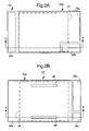
- the substrate 20 contacts the upper major surface 10a of the chip 10 and is referred to herein as the upper substrate; its chip-contacting face 20a is depicted in FIG. 2A.
- the substrate 22 contacts the lower major surface 10b of the chip 10 and is referred to herein as the lower substrate; its chip-contacting face 22a is depicted in FIG. 2B.
- the position of the chip 10 on the upper substrate 20 is designated by the phantom outline 24.
- Three solderable conductor pads 26a, 26b, 26c are formed on the substrate face 20a.
- the pad 26a overlaps the chip conductor pad 12a, but not the chip conductor pad 12b, and extends rightward beyond the outline 24 of chip 10 as viewed in FIG. 2A, to facilitate connection of a first electrical terminal 28 to the FET source.
- the pad 26b overlaps the chip conductor pad 12b, but not the chip conductor pad 12a, and extends rightward beyond the outline 24 of chip 10 as viewed in FIG. 2A, to facilitate connection of a second electrical terminal 30 to the FET gate.
- the pad 26c lies outside the outline 24 of chip 10, and is soldered to the upper surface of a third electrical terminal 32, as shown in FIG. 3A.
- the position of the chip 10 on the lower substrate 22 is designated by the phantom outline 34.
- Three solderable conductor pads 36a, 36b, 36c are formed on the substrate face 22a.
- the pad 36a overlaps the entire outline 34 of the chip 10, and extends leftward beyond the outline 34 of chip 10 as viewed in FIG. 2B, to facilitate connection of the third electrical terminal 32 to the FET drain.
- the pads 36b and 36c lie outside the outline 34 of chip 10, and are respectively soldered to the lower surfaces of the first and second electrical terminals 28 and 30, as shown in FIGS. 3A-3B.
- the lower substrate 22 includes first and second rectangular openings 38, 40 that serve as cooling fluid ports, as explained below.
- FIGS. 3A and 3B depict a complete power semiconductor device package 42 built around the chip 10 of FIGS. 1A-1B.
- the package 42 includes the chip 10; the upper and lower substrates 20, 22; the first, second and third terminals 28, 30, 32; and a single or multi-layer circuit board 44.
- the conductor pads 12a and 12b of the chip 10 are respectively soldered to the conductor pads 26a and 26b of the upper substrate 20, and the conductor pad segments 18 of the chip 10 are soldered to the conductor pad 36a of lower substrate 22.
- the first terminal 28 is soldered on its upper face to the conductor pad 26a of upper substrate 20, and on its lower face to the conductor pad 36b of lower substrate 22; in this way, the first terminal 28 is electrically coupled to the FET source.
- the second terminal 30 is soldered on its upper face to the conductor pad 26b of upper substrate 20, and on its lower face to the conductor pad 36c of lower substrate 22; in this way, the second terminal 30 is electrically coupled to the FET gate.
- the third terminal 32 is soldered on its upper face to the conductor pad 26c of upper substrate 20, and on its lower face to the conductor pad 36a of lower substrate 22; in this way, the third terminal 32 is electrically coupled to the FET drain.
- the terminals 28, 30, 32 are bent downward and pass through suitable openings in the circuit board 44 for attachment to a circuit board conductor, as indicated in FIG. 3 A.
- the circuit board 44 is also provided with first and second rectangular fluid conduits 46 that correspond in shape and alignment with the first and second openings 38, 40 of lower substrate 22.
- the lower substrate 22 is attached to the circuit board 44 with a sealant adhesive or solder 48 that prevents leakage of cooling fluid between the openings 38, 40 and the corresponding fluid conduits 46.
- the location of the chip 10 with respect to the lower substrate 22 is such that the solder joint or conductive adhesive between substrate 22 and the marginal region 16a of chip 10 defines a fluid manifold 49 that encompasses the openings 38, 40 of substrate 22 and the walls 16b of chip 10.
- Cooling fluid is supplied to the fluid manifold 49 through the substrate opening 38 (also referred to herein as inlet port 38) and a first fluid conduit 46 of circuit board 44 that is aligned with the opening 38.
- the cooling fluid spreads out in the manifold 49 passes through the micro-channels 14, and is exhausted through the substrate opening 40 (also referred to herein as outlet port 40) and a second fluid conduit 46 of circuit board 44 that is aligned with the opening 40.
- the fluid conduits 46 of circuit board 44 may be formed in several different ways, as described in related U.S. Patent Application Serial No. 10/XXX,XXX (Attorney Docket No. DP-310178).
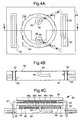
- FIGS. 4A-4C depict a power semiconductor device package 50 incorporating several alternate design features.
- the rectangular substrate openings 38, 40 of package 42 are replaced with a series of square or circular openings for improved coolant flow; the view of FIG. 4C depicts the inlet openings 38a, 38b, 38c, 38d, 38e.
- Inlet and outlet fluid plenums below the substrate openings are formed by the combination of a braze alloy 52 printed on the bottom face of substrate 22 except in the vicinity of the substrate openings and a copper or aluminum plate 54 brazed to the braze alloy 52.
- the alloy-free areas in the vicinity of the substrate openings define inlet and outlet plenums for interfacing the inlet and outlet conduits 58, 60 to the inlet and outlet openings in substrate 22.
- FIGS. 4A-4B illustrate an interface between the plate 54 and the circuit board 44.
- the circuit board 44 is provided with metalized vias 62 for receiving the device terminals 28-32, metalized rings 64 and 66 surrounding the conduits 58 and 60, respectively, and a metalized ring 68 surrounding the rings 64, 66.
- the plate 54 is soldered to the circuit board 44 at metalized rings 64-68, forming a perimeter mechanical support for the device and fluid seals around the conduits 58 and 60.
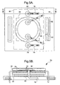
- FIGS. 5A-5B depict a power semiconductor device package 70 in which additional cooling is achieved by supplying coolant to a set of parallel micro-channels 72 formed on the inboard side of upper substrate 20 and surrounded by a fluid manifold 73.
- the construction of the package 70 is similar to that of the package 50, except that the substrates 20, 22 and plate 54 are widened as designated by the reference numeral 82 to accommodate an additional set of fluid conduits 74, 76 laterally outboard of the metalized ring 68 that supply fluid to, and exhaust fluid from, the fluid manifold 73.
- FIG. 1 depict a power semiconductor device package 70 in which additional cooling is achieved by supplying coolant to a set of parallel micro-channels 72 formed on the inboard side of upper substrate 20 and surrounded by a fluid manifold 73.
- the construction of the package 70 is similar to that of the package 50, except that the substrates 20, 22 and plate 54 are widened as designated by the reference numeral 82 to accommodate an additional set of fluid conduits 74,
- the circuit board 44 includes a pair of metalized rings 78, 80 surrounding the fluid conduits 74, 76; the plate 54 has a similar metallization pattern and set of openings, and the plate 54 is soldered to the circuit board 44 at metalized rings 78, 80, forming fluid seals around the conduits 74, 76. Since the fluid conduits 74, 76 are also laterally outboard of the IC chip 10 (the outline of which is designated by the reference numeral 34 in FIG. 5A) a pair of solderable annular spacers having the same thickness as the IC chip 10 are placed in vertical alignment with the fluid conduits 74, 76, in the same plane as the IC chip 10, and soldered to metalized rings formed on the upper and lower substrates 20, 22. In FIG. 5B, the spacer for the fluid conduit 76 is designated by the reference numeral 84.
- FIG. 6 illustrates a further variation of the invention, where a set of parallel micro-channels 90 are formed in the lower substrate 22.
- Liquid coolant can be supplied to and exhausted from the micro-channels 90 as described above in respect to FIGS. 3B-5B.
- the micro-channels 90 may be formed by manufacturing the substrate 22 in upper and lower halves that are joined following or prior to formation of surface features that define the channels and fluid manifolds.
- FIG. 7 depicts a variant of the embodiment of FIG. 6, where set of parallel micro-channels 92 are formed a conductor layer 94 bonded to the lower substrate 22.
- liquid coolant can be supplied to and exhausted from the micro-channels 92 as described above in respect to FIGS. 3B-5B.
- the micro-channels 92 may be formed by multi-step formation of the conductor layer 94.
- FIG. 8 illustrates the invention as applied to a so-called over-mold semiconductor package, where the IC chip 10 is mounted on a metal or ceramic substrate 96, and a moldable plastic or resinous material 98 such as epoxy is molded over chip 10 and all but the bottom face of the substrate 96.
- the substrate 96 can form one of the primary terminals of the IC chip 10, and the other terminals are formed by one or more over-molded terminals 100 attached to the upper face of the IC chip 10 by a wirebond 102, for example.
- a set of parallel micro-channels 104 are formed in the IC chip 10 as in the other embodiments, and a pair of fluid conduits 106 (one of which is shown in FIG. 8) supply coolant fluid to and from the micro-channels 104 as described above.
- the present invention utilizes integral fluid conducting micro-channels to provide improved cooling in a power semiconductor device package. While described in reference to the illustrated embodiments, it is expected that numerous modifications and variations in addition to those mentioned herein will occur to those skilled in the art. For example, the layout and profile of the micro-channels may be different than shown herein, with corresponding changes in the size and configuration of the inlet and outlet ports, and so on. Accordingly, it is intended that the invention not be limited to the disclosed embodiment, but that it have the full scope permitted by the language of the following claims.
Landscapes
- Engineering & Computer Science (AREA)
- Microelectronics & Electronic Packaging (AREA)
- Cooling Or The Like Of Semiconductors Or Solid State Devices (AREA)
- Cooling Or The Like Of Electrical Apparatus (AREA)
Applications Claiming Priority (1)
| Application Number | Priority Date | Filing Date | Title |
|---|---|---|---|
| US10/900,538 US7538425B2 (en) | 2004-07-28 | 2004-07-28 | Power semiconductor package having integral fluid cooling |
Publications (3)
| Publication Number | Publication Date |
|---|---|
| EP1622199A2 true EP1622199A2 (de) | 2006-02-01 |
| EP1622199A3 EP1622199A3 (de) | 2006-03-15 |
| EP1622199B1 EP1622199B1 (de) | 2018-09-12 |
Family
ID=35355751
Family Applications (1)
| Application Number | Title | Priority Date | Filing Date |
|---|---|---|---|
| EP05076556.9A Expired - Lifetime EP1622199B1 (de) | 2004-07-28 | 2005-07-07 | Leistungshalbleiterverpackung mit integrierter Fluidkühlung |
Country Status (2)
| Country | Link |
|---|---|
| US (1) | US7538425B2 (de) |
| EP (1) | EP1622199B1 (de) |
Cited By (3)
| Publication number | Priority date | Publication date | Assignee | Title |
|---|---|---|---|---|
| EP2330873A1 (de) * | 2009-12-03 | 2011-06-08 | Continental Automotive GmbH | Elektronisches Modul |
| US10461017B2 (en) | 2016-08-02 | 2019-10-29 | Infineon Technologies Ag | Package with partially encapsulated cooling channel for cooling an encapsulated chip |
| CN113299618A (zh) * | 2021-04-29 | 2021-08-24 | 中国电子科技集团公司第二十九研究所 | 一种立体集成高效散热封装结构及其制备方法 |
Families Citing this family (41)
| Publication number | Priority date | Publication date | Assignee | Title |
|---|---|---|---|---|
| US7551439B2 (en) * | 2006-03-28 | 2009-06-23 | Delphi Technologies, Inc. | Fluid cooled electronic assembly |
| EP1870687B1 (de) * | 2006-06-23 | 2012-09-12 | STMicroelectronics Srl | Anordnung einer intetriergen Einrichtung mit einer vereinfachten Flüssigkeitsverbindung zu den Bereichen der Einrichtung |
| US7608924B2 (en) * | 2007-05-03 | 2009-10-27 | Delphi Technologies, Inc. | Liquid cooled power electronic circuit comprising stacked direct die cooled packages |
| US7795726B2 (en) | 2007-05-03 | 2010-09-14 | Delphi Technologies, Inc. | Liquid cooled power electronic circuit comprising a stacked array of directly cooled semiconductor chips |
| US7782616B1 (en) | 2009-04-23 | 2010-08-24 | Delphi Technologies, Inc. | Heat-dissipating component having stair-stepped coolant channels |
| US20120095371A1 (en) | 2010-10-18 | 2012-04-19 | CardioSonic Ltd. | Ultrasound transducer and cooling thereof |
| US9566456B2 (en) * | 2010-10-18 | 2017-02-14 | CardioSonic Ltd. | Ultrasound transceiver and cooling thereof |
| US9028417B2 (en) | 2010-10-18 | 2015-05-12 | CardioSonic Ltd. | Ultrasound emission element |
| US20130218068A1 (en) | 2010-10-18 | 2013-08-22 | CardioSonic Ltd. | Therapeutics reservoir |
| WO2012051704A1 (en) | 2010-10-19 | 2012-04-26 | Electronic Motion Systems Holdings Limited | A power module for converting dc to ac |
| US8654541B2 (en) | 2011-03-24 | 2014-02-18 | Toyota Motor Engineering & Manufacturing North America, Inc. | Three-dimensional power electronics packages |
| US10357304B2 (en) | 2012-04-18 | 2019-07-23 | CardioSonic Ltd. | Tissue treatment |
| US11357447B2 (en) | 2012-05-31 | 2022-06-14 | Sonivie Ltd. | Method and/or apparatus for measuring renal denervation effectiveness |
| DE102012212686B4 (de) * | 2012-07-19 | 2016-11-10 | Alfmeier Präzision AG Baugruppen und Systemlösungen | Ventil |
| JP5534067B1 (ja) * | 2013-03-06 | 2014-06-25 | 日本電気株式会社 | 電子部品、および電子部品冷却方法 |
| US10933259B2 (en) | 2013-05-23 | 2021-03-02 | CardioSonic Ltd. | Devices and methods for renal denervation and assessment thereof |
| CN106796477B (zh) * | 2015-02-27 | 2018-05-29 | 株式会社藤仓 | 布线体、布线基板、布线构造体及触摸传感器 |
| CA2978795A1 (en) | 2015-03-16 | 2016-09-22 | Dana Canada Corporation | Heat exchangers with plates having surface patterns for enhancing flatness and methods for manufacturing same |
| US12255123B2 (en) | 2015-09-30 | 2025-03-18 | Microfabrica Inc. | Micro heat transfer arrays, micro cold plates, and thermal management systems for semiconductor devices, and methods for using and making such arrays, plates, and systems |
| US9953899B2 (en) | 2015-09-30 | 2018-04-24 | Microfabrica Inc. | Micro heat transfer arrays, micro cold plates, and thermal management systems for cooling semiconductor devices, and methods for using and making such arrays, plates, and systems |
| US10566265B2 (en) * | 2016-11-18 | 2020-02-18 | Toyota Motor Engineering & Manufacturing North America, Inc. | Electronic assemblies having a cooling chip layer with impingement channels and through substrate vias |
| US20200094080A1 (en) | 2017-03-20 | 2020-03-26 | Sonivie Ltd. | Method for treating heart failure by improving ejection fraction of a patient |
| US10959343B2 (en) * | 2017-08-25 | 2021-03-23 | Hewlett Packard Enterprise Development Lp | Integrated stand-offs for printed circuit boards |
| US11735495B2 (en) * | 2019-02-27 | 2023-08-22 | Intel Corporation | Active package cooling structures using molded substrate packaging technology |
| US11996349B2 (en) * | 2020-05-11 | 2024-05-28 | Dr. Ing. H. C. F. Porsche Ag | Power electronics for an electrical machine, drivetrain, motor vehicle |
| CN113257762B (zh) * | 2021-03-03 | 2022-07-22 | 中国科学院微电子研究所 | 热管理监控模块 |
| CN113517242B (zh) * | 2021-03-03 | 2023-12-19 | 中国科学院微电子研究所 | 热电集成散热模块 |
| US20220406686A1 (en) * | 2021-06-16 | 2022-12-22 | Intel Corporation | Glass-based cavity and channels for cooling of embedded dies and 3d integrated modules using package substrates with glass core |
| US12063763B2 (en) | 2021-09-14 | 2024-08-13 | Hamilton Sundstrand Corporation | Cooling in conductors for chips |
| US12490411B2 (en) | 2022-06-25 | 2025-12-02 | EvansWerks, Inc. | Cooling system and methods |
| US12363864B2 (en) | 2022-06-25 | 2025-07-15 | EvansWerks, Inc. | Cooling system and methods |
| US12452991B2 (en) | 2022-06-25 | 2025-10-21 | EvansWerks, Inc. | Cooling system and methods |
| US12453048B2 (en) | 2022-06-25 | 2025-10-21 | EvansWerks, Inc. | Cooling system and methods |
| US12200908B2 (en) | 2022-06-25 | 2025-01-14 | EvansWerks, Inc. | Cooling system and methods |
| US12101909B2 (en) | 2022-06-25 | 2024-09-24 | EvansWerks, Inc. | Cooling system and methods |
| US12133365B2 (en) | 2022-06-25 | 2024-10-29 | EvansWerks, Inc. | Cooling system and methods |
| US12122251B2 (en) | 2022-09-28 | 2024-10-22 | BorgWarner US Technologies LLC | Systems and methods for bidirectional message architecture for inverter for electric vehicle |
| US12528329B2 (en) | 2023-06-07 | 2026-01-20 | BorgWarner US Technologies LLC | Systems for cooling module assembly for inverter for electric vehicle |
| US12526961B2 (en) | 2023-06-07 | 2026-01-13 | BorgWarner US Technologies LLC | Systems for cooling module assembly for inverter for electric vehicle |
| US12461129B2 (en) | 2023-08-28 | 2025-11-04 | BorgWarner US Technologies LLC | Systems and methods for galvanic interface bond detection for inverter for electric vehicle |
| EP4723809A1 (de) * | 2024-10-06 | 2026-04-08 | LiquaCool IP LLC | Geschlossenes flüssigkeitskühlsystem |
Family Cites Families (7)
| Publication number | Priority date | Publication date | Assignee | Title |
|---|---|---|---|---|
| US3365620A (en) | 1966-06-13 | 1968-01-23 | Ibm | Circuit package with improved modular assembly and cooling apparatus |
| US5901037A (en) * | 1997-06-18 | 1999-05-04 | Northrop Grumman Corporation | Closed loop liquid cooling for semiconductor RF amplifier modules |
| US6175154B1 (en) * | 1997-12-16 | 2001-01-16 | Texas Instruments Incorporated | Fully encapsulated metal leads for multi-level metallization |
| US6796370B1 (en) * | 2000-11-03 | 2004-09-28 | Cray Inc. | Semiconductor circular and radial flow cooler |
| US7032392B2 (en) * | 2001-12-19 | 2006-04-25 | Intel Corporation | Method and apparatus for cooling an integrated circuit package using a cooling fluid |
| US6812553B2 (en) * | 2002-01-16 | 2004-11-02 | Delphi Technologies, Inc. | Electrically isolated and thermally conductive double-sided pre-packaged component |
| US7357898B2 (en) * | 2003-07-31 | 2008-04-15 | Agency For Science, Technology And Research | Microfluidics packages and methods of using same |
-
2004
- 2004-07-28 US US10/900,538 patent/US7538425B2/en not_active Expired - Lifetime
-
2005
- 2005-07-07 EP EP05076556.9A patent/EP1622199B1/de not_active Expired - Lifetime
Cited By (4)
| Publication number | Priority date | Publication date | Assignee | Title |
|---|---|---|---|---|
| EP2330873A1 (de) * | 2009-12-03 | 2011-06-08 | Continental Automotive GmbH | Elektronisches Modul |
| US10461017B2 (en) | 2016-08-02 | 2019-10-29 | Infineon Technologies Ag | Package with partially encapsulated cooling channel for cooling an encapsulated chip |
| CN113299618A (zh) * | 2021-04-29 | 2021-08-24 | 中国电子科技集团公司第二十九研究所 | 一种立体集成高效散热封装结构及其制备方法 |
| CN113299618B (zh) * | 2021-04-29 | 2023-07-14 | 中国电子科技集团公司第二十九研究所 | 一种立体集成高效散热封装结构及其制备方法 |
Also Published As
| Publication number | Publication date |
|---|---|
| EP1622199B1 (de) | 2018-09-12 |
| US7538425B2 (en) | 2009-05-26 |
| EP1622199A3 (de) | 2006-03-15 |
| US20060022334A1 (en) | 2006-02-02 |
Similar Documents
| Publication | Publication Date | Title |
|---|---|---|
| EP1622199B1 (de) | Leistungshalbleiterverpackung mit integrierter Fluidkühlung | |
| US7834448B2 (en) | Fluid cooled semiconductor power module having double-sided cooling | |
| US11145571B2 (en) | Heat transfer for power modules | |
| EP1628345B1 (de) | Eingekapseltes flüssigkeitsgekühltes mikroelektronisches Gehäuse | |
| US7486514B2 (en) | Cooling apparatus with discrete cold plates disposed between a module enclosure and electronics components to be cooled | |
| US7808781B2 (en) | Apparatus and methods for high-performance liquid cooling of multiple chips with disparate cooling requirements | |
| US8232637B2 (en) | Insulated metal substrates incorporating advanced cooling | |
| US7230832B2 (en) | Cooled electronic assembly and method for cooling a printed circuit board | |
| EP1294022B1 (de) | Elektronikmodul mit Kühlsubstrat mit internem Kühlflüssigkeitskreis und verwandte Methode | |
| US20040251530A1 (en) | Three-dimensionally mounted semiconductor module and three-dimensionally mounted semiconductor system | |
| US12368085B2 (en) | Integration of semiconductor device assemblies with thermal dissipation mechanisms | |
| US8860212B1 (en) | Fluid cooled semiconductor die package | |
| US11961782B2 (en) | Integration of semiconductor device assemblies with thermal dissipation mechanisms | |
| TWM667771U (zh) | 電路板結構 | |
| CN112349666B (zh) | 散热型的pcb组装结构及其组装方法 | |
| TWI922031B (zh) | 電路板結構 | |
| CN113517242B (zh) | 热电集成散热模块 | |
| CN112038307B (zh) | 用于功率模块的热传递 | |
| JPH08200911A (ja) | 電気自動車用冷却装置 |
Legal Events
| Date | Code | Title | Description |
|---|---|---|---|
| PUAI | Public reference made under article 153(3) epc to a published international application that has entered the european phase |
Free format text: ORIGINAL CODE: 0009012 |
|
| PUAL | Search report despatched |
Free format text: ORIGINAL CODE: 0009013 |
|
| AK | Designated contracting states |
Kind code of ref document: A2 Designated state(s): AT BE BG CH CY CZ DE DK EE ES FI FR GB GR HU IE IS IT LI LT LU LV MC NL PL PT RO SE SI SK TR |
|
| AX | Request for extension of the european patent |
Extension state: AL BA HR MK YU |
|
| AK | Designated contracting states |
Kind code of ref document: A3 Designated state(s): AT BE BG CH CY CZ DE DK EE ES FI FR GB GR HU IE IS IT LI LT LU LV MC NL PL PT RO SE SI SK TR |
|
| AX | Request for extension of the european patent |
Extension state: AL BA HR MK YU |
|
| 17P | Request for examination filed |
Effective date: 20060915 |
|
| 17Q | First examination report despatched |
Effective date: 20061024 |
|
| AKX | Designation fees paid |
Designated state(s): AT BE BG CH CY CZ DE DK EE ES FI FR GB GR HU IE IS IT LI LT LU LV MC NL PL PT RO SE SI SK TR |
|
| REG | Reference to a national code |
Ref country code: DE Ref legal event code: R079 Ref document number: 602005054587 Country of ref document: DE Free format text: PREVIOUS MAIN CLASS: H01L0023460000 Ipc: H01L0023433000 |
|
| RIC1 | Information provided on ipc code assigned before grant |
Ipc: H01L 23/473 20060101ALI20180212BHEP Ipc: H05K 1/02 20060101ALI20180212BHEP Ipc: H01L 23/00 20060101ALI20180212BHEP Ipc: H01L 29/06 20060101ALI20180212BHEP Ipc: H01L 23/433 20060101AFI20180212BHEP |
|
| GRAP | Despatch of communication of intention to grant a patent |
Free format text: ORIGINAL CODE: EPIDOSNIGR1 |
|
| STAA | Information on the status of an ep patent application or granted ep patent |
Free format text: STATUS: GRANT OF PATENT IS INTENDED |
|
| INTG | Intention to grant announced |
Effective date: 20180412 |
|
| GRAS | Grant fee paid |
Free format text: ORIGINAL CODE: EPIDOSNIGR3 |
|
| GRAA | (expected) grant |
Free format text: ORIGINAL CODE: 0009210 |
|
| STAA | Information on the status of an ep patent application or granted ep patent |
Free format text: STATUS: THE PATENT HAS BEEN GRANTED |
|
| REG | Reference to a national code |
Ref country code: DE Ref legal event code: R081 Ref document number: 602005054587 Country of ref document: DE Owner name: DELPHI TECHNOLOGIES IP LIMITED, BB Free format text: FORMER OWNER: DELPHI TECHNOLOGIES, INC., TROY, MICH., US |
|
| AK | Designated contracting states |
Kind code of ref document: B1 Designated state(s): AT BE BG CH CY CZ DE DK EE ES FI FR GB GR HU IE IS IT LI LT LU LV MC NL PL PT RO SE SI SK TR |
|
| REG | Reference to a national code |
Ref country code: GB Ref legal event code: FG4D |
|
| REG | Reference to a national code |
Ref country code: CH Ref legal event code: EP |
|
| REG | Reference to a national code |
Ref country code: IE Ref legal event code: FG4D |
|
| REG | Reference to a national code |
Ref country code: DE Ref legal event code: R096 Ref document number: 602005054587 Country of ref document: DE |
|
| REG | Reference to a national code |
Ref country code: AT Ref legal event code: REF Ref document number: 1041591 Country of ref document: AT Kind code of ref document: T Effective date: 20181015 |
|
| REG | Reference to a national code |
Ref country code: NL Ref legal event code: MP Effective date: 20180912 |
|
| REG | Reference to a national code |
Ref country code: LT Ref legal event code: MG4D |
|
| PG25 | Lapsed in a contracting state [announced via postgrant information from national office to epo] |
Ref country code: BG Free format text: LAPSE BECAUSE OF FAILURE TO SUBMIT A TRANSLATION OF THE DESCRIPTION OR TO PAY THE FEE WITHIN THE PRESCRIBED TIME-LIMIT Effective date: 20181212 Ref country code: SE Free format text: LAPSE BECAUSE OF FAILURE TO SUBMIT A TRANSLATION OF THE DESCRIPTION OR TO PAY THE FEE WITHIN THE PRESCRIBED TIME-LIMIT Effective date: 20180912 Ref country code: LT Free format text: LAPSE BECAUSE OF FAILURE TO SUBMIT A TRANSLATION OF THE DESCRIPTION OR TO PAY THE FEE WITHIN THE PRESCRIBED TIME-LIMIT Effective date: 20180912 Ref country code: FI Free format text: LAPSE BECAUSE OF FAILURE TO SUBMIT A TRANSLATION OF THE DESCRIPTION OR TO PAY THE FEE WITHIN THE PRESCRIBED TIME-LIMIT Effective date: 20180912 Ref country code: GR Free format text: LAPSE BECAUSE OF FAILURE TO SUBMIT A TRANSLATION OF THE DESCRIPTION OR TO PAY THE FEE WITHIN THE PRESCRIBED TIME-LIMIT Effective date: 20181213 |
|
| REG | Reference to a national code |
Ref country code: DE Ref legal event code: R081 Ref document number: 602005054587 Country of ref document: DE Owner name: DELPHI TECHNOLOGIES IP LIMITED, BB Free format text: FORMER OWNER: DELPHI TECHNOLOGIES, INC., TROY, MICH., US |
|
| PG25 | Lapsed in a contracting state [announced via postgrant information from national office to epo] |
Ref country code: ES Free format text: LAPSE BECAUSE OF FAILURE TO SUBMIT A TRANSLATION OF THE DESCRIPTION OR TO PAY THE FEE WITHIN THE PRESCRIBED TIME-LIMIT Effective date: 20180912 Ref country code: LV Free format text: LAPSE BECAUSE OF FAILURE TO SUBMIT A TRANSLATION OF THE DESCRIPTION OR TO PAY THE FEE WITHIN THE PRESCRIBED TIME-LIMIT Effective date: 20180912 |
|
| REG | Reference to a national code |
Ref country code: AT Ref legal event code: MK05 Ref document number: 1041591 Country of ref document: AT Kind code of ref document: T Effective date: 20180912 |
|
| PG25 | Lapsed in a contracting state [announced via postgrant information from national office to epo] |
Ref country code: EE Free format text: LAPSE BECAUSE OF FAILURE TO SUBMIT A TRANSLATION OF THE DESCRIPTION OR TO PAY THE FEE WITHIN THE PRESCRIBED TIME-LIMIT Effective date: 20180912 Ref country code: NL Free format text: LAPSE BECAUSE OF FAILURE TO SUBMIT A TRANSLATION OF THE DESCRIPTION OR TO PAY THE FEE WITHIN THE PRESCRIBED TIME-LIMIT Effective date: 20180912 Ref country code: AT Free format text: LAPSE BECAUSE OF FAILURE TO SUBMIT A TRANSLATION OF THE DESCRIPTION OR TO PAY THE FEE WITHIN THE PRESCRIBED TIME-LIMIT Effective date: 20180912 Ref country code: IT Free format text: LAPSE BECAUSE OF FAILURE TO SUBMIT A TRANSLATION OF THE DESCRIPTION OR TO PAY THE FEE WITHIN THE PRESCRIBED TIME-LIMIT Effective date: 20180912 Ref country code: CZ Free format text: LAPSE BECAUSE OF FAILURE TO SUBMIT A TRANSLATION OF THE DESCRIPTION OR TO PAY THE FEE WITHIN THE PRESCRIBED TIME-LIMIT Effective date: 20180912 Ref country code: RO Free format text: LAPSE BECAUSE OF FAILURE TO SUBMIT A TRANSLATION OF THE DESCRIPTION OR TO PAY THE FEE WITHIN THE PRESCRIBED TIME-LIMIT Effective date: 20180912 Ref country code: IS Free format text: LAPSE BECAUSE OF FAILURE TO SUBMIT A TRANSLATION OF THE DESCRIPTION OR TO PAY THE FEE WITHIN THE PRESCRIBED TIME-LIMIT Effective date: 20190112 Ref country code: PL Free format text: LAPSE BECAUSE OF FAILURE TO SUBMIT A TRANSLATION OF THE DESCRIPTION OR TO PAY THE FEE WITHIN THE PRESCRIBED TIME-LIMIT Effective date: 20180912 |
|
| PG25 | Lapsed in a contracting state [announced via postgrant information from national office to epo] |
Ref country code: SK Free format text: LAPSE BECAUSE OF FAILURE TO SUBMIT A TRANSLATION OF THE DESCRIPTION OR TO PAY THE FEE WITHIN THE PRESCRIBED TIME-LIMIT Effective date: 20180912 Ref country code: PT Free format text: LAPSE BECAUSE OF FAILURE TO SUBMIT A TRANSLATION OF THE DESCRIPTION OR TO PAY THE FEE WITHIN THE PRESCRIBED TIME-LIMIT Effective date: 20190112 |
|
| REG | Reference to a national code |
Ref country code: DE Ref legal event code: R097 Ref document number: 602005054587 Country of ref document: DE |
|
| PLBE | No opposition filed within time limit |
Free format text: ORIGINAL CODE: 0009261 |
|
| STAA | Information on the status of an ep patent application or granted ep patent |
Free format text: STATUS: NO OPPOSITION FILED WITHIN TIME LIMIT |
|
| PG25 | Lapsed in a contracting state [announced via postgrant information from national office to epo] |
Ref country code: DK Free format text: LAPSE BECAUSE OF FAILURE TO SUBMIT A TRANSLATION OF THE DESCRIPTION OR TO PAY THE FEE WITHIN THE PRESCRIBED TIME-LIMIT Effective date: 20180912 |
|
| 26N | No opposition filed |
Effective date: 20190613 |
|
| PG25 | Lapsed in a contracting state [announced via postgrant information from national office to epo] |
Ref country code: SI Free format text: LAPSE BECAUSE OF FAILURE TO SUBMIT A TRANSLATION OF THE DESCRIPTION OR TO PAY THE FEE WITHIN THE PRESCRIBED TIME-LIMIT Effective date: 20180912 |
|
| PG25 | Lapsed in a contracting state [announced via postgrant information from national office to epo] |
Ref country code: MC Free format text: LAPSE BECAUSE OF FAILURE TO SUBMIT A TRANSLATION OF THE DESCRIPTION OR TO PAY THE FEE WITHIN THE PRESCRIBED TIME-LIMIT Effective date: 20180912 |
|
| REG | Reference to a national code |
Ref country code: CH Ref legal event code: PL |
|
| GBPC | Gb: european patent ceased through non-payment of renewal fee |
Effective date: 20190707 |
|
| PG25 | Lapsed in a contracting state [announced via postgrant information from national office to epo] |
Ref country code: TR Free format text: LAPSE BECAUSE OF FAILURE TO SUBMIT A TRANSLATION OF THE DESCRIPTION OR TO PAY THE FEE WITHIN THE PRESCRIBED TIME-LIMIT Effective date: 20180912 |
|
| REG | Reference to a national code |
Ref country code: BE Ref legal event code: MM Effective date: 20190731 |
|
| PG25 | Lapsed in a contracting state [announced via postgrant information from national office to epo] |
Ref country code: GB Free format text: LAPSE BECAUSE OF NON-PAYMENT OF DUE FEES Effective date: 20190707 |
|
| PG25 | Lapsed in a contracting state [announced via postgrant information from national office to epo] |
Ref country code: LU Free format text: LAPSE BECAUSE OF NON-PAYMENT OF DUE FEES Effective date: 20190707 Ref country code: CH Free format text: LAPSE BECAUSE OF NON-PAYMENT OF DUE FEES Effective date: 20190731 Ref country code: LI Free format text: LAPSE BECAUSE OF NON-PAYMENT OF DUE FEES Effective date: 20190731 Ref country code: BE Free format text: LAPSE BECAUSE OF NON-PAYMENT OF DUE FEES Effective date: 20190731 |
|
| PG25 | Lapsed in a contracting state [announced via postgrant information from national office to epo] |
Ref country code: FR Free format text: LAPSE BECAUSE OF NON-PAYMENT OF DUE FEES Effective date: 20190731 |
|
| PG25 | Lapsed in a contracting state [announced via postgrant information from national office to epo] |
Ref country code: IE Free format text: LAPSE BECAUSE OF NON-PAYMENT OF DUE FEES Effective date: 20190707 |
|
| PG25 | Lapsed in a contracting state [announced via postgrant information from national office to epo] |
Ref country code: CY Free format text: LAPSE BECAUSE OF FAILURE TO SUBMIT A TRANSLATION OF THE DESCRIPTION OR TO PAY THE FEE WITHIN THE PRESCRIBED TIME-LIMIT Effective date: 20180912 |
|
| PG25 | Lapsed in a contracting state [announced via postgrant information from national office to epo] |
Ref country code: HU Free format text: LAPSE BECAUSE OF FAILURE TO SUBMIT A TRANSLATION OF THE DESCRIPTION OR TO PAY THE FEE WITHIN THE PRESCRIBED TIME-LIMIT; INVALID AB INITIO Effective date: 20050707 |
|
| P01 | Opt-out of the competence of the unified patent court (upc) registered |
Effective date: 20230327 |
|
| PGFP | Annual fee paid to national office [announced via postgrant information from national office to epo] |
Ref country code: DE Payment date: 20240613 Year of fee payment: 20 |
|
| REG | Reference to a national code |
Ref country code: DE Ref legal event code: R071 Ref document number: 602005054587 Country of ref document: DE |