EP1622352A1 - Mehrfach-Funktions-Gerät - Google Patents
Mehrfach-Funktions-Gerät Download PDFInfo
- Publication number
- EP1622352A1 EP1622352A1 EP05254661A EP05254661A EP1622352A1 EP 1622352 A1 EP1622352 A1 EP 1622352A1 EP 05254661 A EP05254661 A EP 05254661A EP 05254661 A EP05254661 A EP 05254661A EP 1622352 A1 EP1622352 A1 EP 1622352A1
- Authority
- EP
- European Patent Office
- Prior art keywords
- model
- main board
- board
- sub
- identification information
- Prior art date
- Legal status (The legal status is an assumption and is not a legal conclusion. Google has not performed a legal analysis and makes no representation as to the accuracy of the status listed.)
- Granted
Links
- 230000006870 function Effects 0.000 claims abstract description 243
- 230000002093 peripheral effect Effects 0.000 claims abstract description 9
- 238000000034 method Methods 0.000 claims description 57
- 238000004519 manufacturing process Methods 0.000 claims description 27
- 238000006467 substitution reaction Methods 0.000 claims description 3
- 239000013256 coordination polymer Substances 0.000 description 84
- 230000015654 memory Effects 0.000 description 27
- 230000007257 malfunction Effects 0.000 description 7
- 238000010586 diagram Methods 0.000 description 6
- 230000005540 biological transmission Effects 0.000 description 5
- 239000011159 matrix material Substances 0.000 description 5
- 230000000994 depressogenic effect Effects 0.000 description 3
- 238000012423 maintenance Methods 0.000 description 3
- 238000004891 communication Methods 0.000 description 2
- 230000002950 deficient Effects 0.000 description 2
- 238000006243 chemical reaction Methods 0.000 description 1
- 238000004590 computer program Methods 0.000 description 1
- 238000010348 incorporation Methods 0.000 description 1
- 239000004973 liquid crystal related substance Substances 0.000 description 1
- 238000012986 modification Methods 0.000 description 1
- 230000004048 modification Effects 0.000 description 1
- 238000012545 processing Methods 0.000 description 1
Images


Classifications
-
- H—ELECTRICITY
- H04—ELECTRIC COMMUNICATION TECHNIQUE
- H04N—PICTORIAL COMMUNICATION, e.g. TELEVISION
- H04N1/00—Scanning, transmission or reproduction of documents or the like, e.g. facsimile transmission; Details thereof
- H04N1/0035—User-machine interface; Control console
- H04N1/00352—Input means
- H04N1/00395—Arrangements for reducing operator input
-
- H—ELECTRICITY
- H04—ELECTRIC COMMUNICATION TECHNIQUE
- H04N—PICTORIAL COMMUNICATION, e.g. TELEVISION
- H04N1/00—Scanning, transmission or reproduction of documents or the like, e.g. facsimile transmission; Details thereof
- H04N1/0083—Arrangements for transferring signals between different components of the apparatus, e.g. arrangements of signal lines or cables
-
- H—ELECTRICITY
- H04—ELECTRIC COMMUNICATION TECHNIQUE
- H04N—PICTORIAL COMMUNICATION, e.g. TELEVISION
- H04N1/00—Scanning, transmission or reproduction of documents or the like, e.g. facsimile transmission; Details thereof
- H04N1/00885—Power supply means, e.g. arrangements for the control of power supply to the apparatus or components thereof
- H04N1/00888—Control thereof
-
- H—ELECTRICITY
- H04—ELECTRIC COMMUNICATION TECHNIQUE
- H04N—PICTORIAL COMMUNICATION, e.g. TELEVISION
- H04N1/00—Scanning, transmission or reproduction of documents or the like, e.g. facsimile transmission; Details thereof
- H04N1/00962—Input arrangements for operating instructions or parameters, e.g. updating internal software
-
- H—ELECTRICITY
- H04—ELECTRIC COMMUNICATION TECHNIQUE
- H04N—PICTORIAL COMMUNICATION, e.g. TELEVISION
- H04N1/00—Scanning, transmission or reproduction of documents or the like, e.g. facsimile transmission; Details thereof
- H04N1/00885—Power supply means, e.g. arrangements for the control of power supply to the apparatus or components thereof
Definitions
- aspects of the invention relate to a multi function device (MFD), particularly to the MFD that is configured such that an appropriate setting for a combination of a main board and a panel board can be automatically made without input from a user.
- MFD multi function device
- Multi function devices having a plurality of functions such as a function of a facsimile device are known. Due to recent customer demands for increased number of functions, a variety of models from low-grade models to high-grade models have been produced. In such variety of models, operation panels corresponding to the grade of the models are provided, respectively. The operation panel in each MFD is controlled by a panel board, which is connected to and controlled by a main board.
- Fig. 12 shows a flowchart illustrating a conventionally employed procedure of inputting a setting regarding a combination of the main board and panel board of the MFD.
- the procedure shown in Fig. 12 is executed when the MFD is powered ON.
- the process judges whether an operation mode of the MFD has been set to a maintenance mode. If the process determines that the operation mode is set to the maintenance mode (S 101: YES), the process writes a model information input by the user (i.e., information representing the model of the MFD) in an EEPROM (Electrically Erasable Programmable Read Only Memory) built in the MFD.
- EEPROM Electrical Erasable Programmable Read Only Memory
- the process retrieves the stored model information from the EEPROM (S103). Then, in S104, the process identifies the model of the operation panel based on the retrieved model information, and sets a key-matrix corresponding to the identified model of the operation panel. After the setting of the key-matrix in S104, the process proceeds to a standby mode. As a result of steps S103 and S104, operations of the operation panel are interpreted correctly, which correspond to the model of the operation panel, and thus the MFD operates correctly.
- the model information manually input by the user is typically a numeral code consisting of a plurality of digits (e.g., four digits) of numbers.
- a numeral code consisting of a plurality of digits (e.g., four digits) of numbers.
- To input such a numeral code for each MFD is very troublesome. Further, since the numeral code is input by the user, there occurs an input error, which results in defective products. However, as far as the numeral code is input manually, there remains a possibility of an erroneous input.
- aspects of the present invention provide an improved MFD in which settings regarding a proper combination of the main board and the panel board can be made without requiring data input by a user.
- a multi function device which is provided with a main board configured to control functions corresponding to a model of the multi function device, a sub board configured to be connected with the main board, the sub board carrying out peripheral control corresponding to the model of the multi function device, a function information storage configured to store function information enabling a combination of the main board and sub board corresponding to the model of the multi function device to function appropriately for each model of the multi function device, a main board first identification information obtaining system that obtains main board first identification information indicative of a category of the main board, a main board second identification information obtaining system that obtains main board second identification information which the main board peculiarly includes for each model of the multi function device, a model identifying system configured to identify the model of the multi function device based on the main board first identification information obtained by the main board first identification information obtaining system and the main board second identification information obtained by the main board second information obtaining system when the multi function device is powered on, a function information obtaining system that obtains function information corresponding to
- the MFD configured above may include the main board that mainly controls functions corresponding to the model of the MFD, and the sub board, which is connected to the main board and operates in accordance with instructions transmitted from the main board, may carry out peripheral control.
- the function information enabling the combination of the main board and sub board, which combination is determined for each model of the MFD, to function appropriately is stored in the function information storing system.
- the model of the MFD is identified based on the main board first identification information and the main board second identification information. Then, the model information corresponding to the thus identified model is obtained from the function information storing system by the function information obtaining system.
- the main board and the sub board are controlled to operate normally.
- a relationship between the main board and the sub board can be identified based on the category of the main board and the information intrinsic to the sub board.
- necessary settings can be automatically carried out and the main board and the sub board function normally. Since the correspondence between the main board and the sub board can be made automatically, troublesome work therefor, which has been required in conventional devices, can be avoided. Further, since the setting is carried out automatically, occurrence of an error due to mistakes of the user can also be avoided.
- the model of the MFD is identified based on the combination of the main board fist identification information and the main board second identification information, the number of distinguishable models may increase, and a variety of models can be identified accurately despite the high number of models.
- the main board may include a model identifying circuit configured to output a voltage intrinsic to the model, and a main board voltage reading system that reads an AD converted value of the voltage output by the model identifying circuit.
- the main board second identification information obtained by the main board second identification information obtaining system may be the AD converted value of the voltage read by the main board voltage reading system.
- the AD converted value of the voltage output by the model identifying circuit is referred to.
- the model can be identified based on a hardware configuration, that is, the correspondence between the main board and the sub board can be made based on the hardware configuration. Therefore, a troublesome work such as the user's input of data can be avoided, and accordingly, malfunctions due to erroneous input of the user can be avoided.
- the AD converted value is used, the output voltage of the model identifying circuit can be detected at a high resolution. As a result, identification of the model can be realized at the high resolution.
- a sub board first identification information obtaining system configured to obtain sub board first identification information the sub board peculiarly includes, a sub device identification system configured to identify the sub device based on the sub board first identification information obtained by the sub board first identification information obtaining system when the multi function device is powered on, a coincidence judging system configured to judge whether the sub device identified by the sub device identifying system coincides with the sub device of the identified model of the multi function device identified by the model identifying system.
- the function information obtaining system may obtain the function information corresponding to the model identified by the model identifying system from the function information storing system if the coincidence judging system determines that the sub device identified by the sub device identifying system coincides with the sub device of the identified model of the multi function device identified by the model identifying system.
- the sub device when the MFD is powered ON, the sub device is identified based on the sub board first identification information. Then, it is judges whether the thus identified sub device coincides with the sub device to be used in the model identified by the model identifying system. If they coincide with each other, the function information corresponding to the identified model is obtained from the function information storing system. Then, the main board and the sub board are controlled to operate normally. Since it is judged whether the model identified based on the information from the main board is correct or not by identifying the sub device based on the information obtained from the sub board, the relationship between the main board and the sub board may be examined accurately. As a result, malfunctions due to inappropriate combination of the main board and the sub board can be suppressed effectively.
- the sub board may include a sub device identifying circuit configured to output a voltage intrinsic to the sub device controlled by the sub board, and a sub board voltage reading system configured to read an AD converted value of the voltage output by the sub device identifying circuit.
- the sub board first identification information obtained by the sub board first identification information obtaining system may include the AD converted value of the voltage read by the sub board voltage reading system.
- the AD converted value of the voltage output by the sub device identifying circuit which outputs the voltage intrinsic to the sub device controlled by the sub board is recognized. Therefore, the sub device can be identified based on the hardware configuration, and thus whether the model identified based on the information obtained from the main board is correct is judged automatically. Thus, the malfunction of the MFD due to human errors can be avoided. Further, since the AD value is used as the sub board first identification information, the identification information can be obtained at a high resolution. Consequently, the identification of the sub device can be done at a high accuracy.
- the multi function system may further include a sub board second identification information obtaining system that obtains sub board second identification information that identifies a category of the sub board.
- the sub device identifying system may identify a sub device based on the sub board first identification information obtained by the sub board first identification information obtaining system and the sub board second identification information obtained by the sub board second identification information obtaining system when the multi function device is powered on.
- the sub device when the MFD is powered ON, the sub device is identified based on the sub board first identification information and the sub board second identification information. Since the sub device is identified based on the combination of the sub board first identification information and the sub board second identification information, the number of distinguishable sub devices increase, and even if the variety of sub devices should be identified, it can be done at high accuracy.
- the multi function device may further include an error notifying system configured to notify an occurrence of an error when the sub device identified by the sub device identifying system and the sub device of the model identified by the model identifying system are determined to be different by the coincidence judging system.
- an error notifying system configured to notify an occurrence of an error when the sub device identified by the sub device identifying system and the sub device of the model identified by the model identifying system are determined to be different by the coincidence judging system.
- the user when the error is notified, the user can recognize that the MFD is not operating correctly. Therefore, the user can redo the correlation between the main board and the sub board, or as the manufacture to fix the MFD immediately.
- the sub device may include a substitute model storing system configured to store a substitute model which is used as the model identified by the model identifying system if the sub device is identified by the sub device identifying system, if the model cannot be identified based on the model identification information, and a model substituting system that uses the model stored in the substitution model storing system as the model identified by the model identification system if the model cannot be identified based on the model identification information when the sub device is identified by the sub device identifying system.
- a substitute model storing system configured to store a substitute model which is used as the model identified by the model identifying system if the sub device is identified by the sub device identifying system, if the model cannot be identified based on the model identification information, and a model substituting system that uses the model stored in the substitution model storing system as the model identified by the model identification system if the model cannot be identified based on the model identification information when the sub device is identified by the sub device identifying system.
- the substitute model stored in the substituted model storing system is used as the model identified by the model identifying system.
- the substitute model may be the model having the largest production number among the models corresponding to the identified sub device. In such a case, a possibility that the basic function of the MFD does not work can be reduced. If the basic function is available, the resetting operation can be carried out relatively easily.
- the multi function device may further include a substitute model storing system that stores a substitute model, which is used as the model identified by the model identifying system if the model cannot be identified by the model identifying system, and a substituting system that substitute the substitute model stored in the substitute model storing system as the model identified by the model identifying system if the model cannot be identified by the model identifying system.
- the substitute model stored in the substituted model storing system may be used as the model identified by the mole identifying system.
- the substitute model may be the model of the MFD having the largest production number. In such a case, a possibility that the basic function of the MFD does not work can be reduced. If the basic function is available, the resetting operation can be carried out relatively easily.
- the main board may include a model identifying circuit configured to output a voltage intrinsic to the model, and a main board voltage reading system that reads an AD converted value of the voltage output by the model identifying circuit.
- the main board second identification information obtained by the main board second identification information obtaining system may be the AD converted value of the voltage read by the main board voltage reading system.
- the substitute model stored in the substitute model storing system may be a model having the larges production number. If the model identifying system cannot identify the model as the AD converted value obtained by the main board second identification information obtaining system is indefinite, the substituting system may use the model having the largest production number as the model identified by the model identifying system.
- the AD converted value of the voltage output by the model identifying circuit is used as the main board second identification information. If the AD converted value is indefinite and the model identifying system cannot identify the model, the substitute model, which has the model having the largest production number, may be used as the model identified by the model identifying system. Therefore, even if the model cannot be identified as the AD converted value of the voltage is indefinite, by use of the model having the largest production number, a possibility that the basic function does not work can be reduced. If the basic function is available, the resetting operation can be carried out relatively easily.
- the sub device may be an operation panel through which operations corresponding to the model can be instructed, and the function information may include information regarding settings of the operation panel.
- the function information enabling the combination of the main board and the sub board to function normally may include the setting of the operation panel for inputting instructions corresponding to the model. Since the setting of the operation panel, which may be different among models, can be automatically set by the main board, malfunctions due to setting errors by a user can be avoided.
- the sub device may be an operation panel including at least one of a displaying unit configured to display an indication corresponding to the model and a notifying unit configured to output notification corresponding to the model, and the function information may include setting information of the at least one of the displaying unit and the notifying unit.
- the function information enabling the combination of the main board and the sub board to function normally may include the setting of the displaying unit and/or notifying unit. Since the setting of the operation panel, which may be different among models, can be automatically set by the main board, malfunctions of the display unit/notifying unit due to setting errors by a user can be avoided.
- a method of carrying out function setting for a multi function device including a main board configured to control functions corresponding to a model of the multi function device and a sub board configured to be connected with the main board, the sub board carrying out peripheral control corresponding to the model of the multi function device.
- the method may include the steps of obtaining main board first identification information indicative of a category of the main board, obtaining main board second identification information intrinsic to each model of the multi function device, identifying the model of the multi function device based on the main board first identification information and the main board second identification information when the multi function device is powered on, obtaining function information corresponding to the identified model, and controlling the main board and the sub board of the multi function device to correctly function based on the function information.
- a computer program product comprising computer readable instructions which cause a computer to carry out function setting for a multi function device including a main board configured to control functions corresponding to a model of the multi function device and a sub board configured to be connected with the main board, the sub board carrying out peripheral control corresponding to the model of the multi function device.
- the instructions may cause the computer to obtain main board first identification information indicative of a category of the main board, to obtain main board second identification information intrinsic to each model of the multi function device, to identify the model of the multi function device based on the main board first identification information and the main board second identification information when the multi function device is powered on, to obtain function information corresponding to the identified model, and to control the main board and the sub board of the multi function device to correctly function based on the function information.
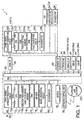
- Figs. 1 and 2 are block diagrams of the MFDs according to the first embodiment.
- Fig. 1 shows a block diagram of an electrical configuration, in which a main board M1 is employed as a main board M
- Fig. 2 shows a block diagram of an electrical configuration in which a main board M2 is used as the main board.
- the MFD is configured such that a plurality of functions (including a facsimile function, a voice communication function using a telephone line 100, and a printer function) are implemented in a single device.
- the MFD 1 includes a main board M (M1), a panel board P (P1), a scanner unit 22, a printer unit 24, a modem 26, a line control unit 28, a parallel interface (I/F) 40, a USB (Universal Serial Bus) I/F 42, a LAN (Local Area Network) I/F 44, a panel I/F 46, an operation unit 34, an LCD 36 and a speaker unit 38.
- An operation panel CP is provided with the operation unit 34, the LCD 36 and the speaker unit 38.
- the main board M is a board that functions to control entire operation of the MFD 1.
- Fig. 1 shows the main board M1
- Fig. 2 shows a main board M2.
- the main board M (main board M1) is provided with a CPU (Central Processing Unit) 12 that controls the entire operation of the MFD 1, a ROM (Read Only Memory) 14 that stores various control programs to be executed by the CPU 12 and fixed value data, a RAM (Random Access Memory) 16 that temporarily stores data and programs necessary for various operations, an EEPROM 18 is a non-volatile memory that stores various pieces of data and setting parameters set by the user, a main board category identifying circuit 62 configured to identify a category of the main board M, a model identifying circuit 64 configured to identify a model of the MFD 1, an AD converter 66 connected to the model identifying circuit 64 and converts a voltage value output by the model identifying circuit 64 to a digital signal, and an ASIC (Application Specific Integrated Circuit) 52.
- a CPU Central Processing Unit
- ROM Read Only Memory
- RAM Random Access Memory
- an EEPROM 18 is a non-volatile memory that stores various pieces of data and setting parameters set by the user
- the ROM 14 stores a function table memory 14a and a substitute model memory 14b.
- the function table memory 14a stores a function table indicating proper combinations of a main board M and a panel board P connected to the main board M in the MFD 1, for each model of the MFD 1.
- a function table corresponding to the model of the MFD 1 from among the function information stored in the function table memory 14a is obtained based on hardware information of the main board M and the panel board P.
- respective units i.e., the operation unit 34, LCD 36 and speaker unit 38
- the substitute model memory 14b is a memory storing substitute models, which can be used if the model cannot be identified based on the hardware information of the main board M and panel board P.
- the substitute model memory 14b stores, as the substitute models, the model having the maximum production is stored.
- the model cannot be identified based on the hardware information regarding the main board M and the panel board P, by using the configuration of the model having the maximum production stored in the substitute model memory 14b, at least the basic functions of the operation panel CP can be used.
- a model having the maximum production is selected from among the models corresponding to the identified operation panel CP with reference to the substitute model memory 14b, a possibility that the basic functions would not work can be reduced. It should be noted that, if the basic functions can be used, a re-setting operation thereafter can be performed relatively easily.
- the scanner unit 22 which is controlled by the main board M, scans an original set at a predetermined scanning position (not shown) to capture an image of the original and generates image data representing the captured image under control by the CPU 12.
- the scanner unit 22 is provided with an original feeding motor (not shown).
- the printer unit 24 includes an inkjet printer that prints out images on a recording sheet set at a predetermined sheet feed position (not shown) under control of the CPU 12.
- the printer unit 24 includes a sheet feeding motor (not shown), a print head (not shown) ejecting ink drops to the recording sheet, and a carriage motor (not shown) that moves a carriage (not shown) mounting the print head.
- the modem 26 modulates, under control of the CPU 12, the image data generated by the scanner unit 22 to generates image signal which can be transmitted to the telephone line network 100 via the line control unit 28, and also demodulates the image signal received from the telephone line network 100 via the network control unit 28 to generate the image data.
- the network control unit 28 receives/transmits various signals from/to the telephone line 100. Further, the network control unit 28 sets, under control of the CPU 12, the transmission path which serves as destination/origin of the signals received from/transmitted to the telephone line 100.
- a path directed to the modem 26 is set, when the operation unit 34 is operated to transmit the image (i.e., facsimile data) or when the image signal (i.e., facsimile data) is received from the telephone line 100.
- the transmission path set as above is released when the output of the image signal by the modem 26 has been completed, or when the reception of the image signal from the telephone line network 100 has been completed, and thereafter, the image signal cannot be transmitted through the transmission path.
- the main board category identifying circuit 62 includes, at least, a DC (direct current) power source unit (not shown), a first resistance unit (not shown) provided between the DC power source unit and a port A 12a provided to the CPU 12, a second resistance unit (not shown) provided between the DC power source unit and a port B 12b provided to the CPU 12, and an earth unit (not shown).
- a DC (direct current) power source unit not shown
- a first resistance unit not shown
- the DC power source unit provided between the DC power source unit and a port A 12a provided to the CPU 12
- a second resistance unit not shown
- the output signal is set to ON (High level) or OFF (Low level).
- the setting of the output signal (ON/OFF) is determined when the main board M is manufactured.
- a combination of the output signals to the port A 12a and port B 12b is determined in accordance with the category (one of four categories) of the main board M (one of M1-M4).
- the model identifying circuit 64 is configured such that voltages intrinsic to respective models are output.
- the model identifying circuit 64 includes a DC power source unit (not shown), an earth unit (not shown), a fixed resistance unit (not shown) and a variable resistance unit (not shown) which are provided, in series, between the earth unit and the DC power source unit, and a voltage is output to the AD converter 66 from a point between the fixed resistance unit and the variable resistance unit.
- the voltage output to the AD converter 66 can be adjusted by changing a resistance value of the variable resistance unit, and the resistance value is set for each model. Since the voltage value intrinsic to each model is output to the AD converter 66, the model of the MFD 1 can be identified by reading the AD value of the voltage input to the AD converter 66.
- the CPU 12, the ROM 14, the RAM 16, the EEPROM 18, the AD converter 66, the ASIC 52, and the modem 26 are interconnected through a main bus 54.
- the main board category identifying circuit 62 is connected the two port, the port A 12a, and the port B 12b provided to the CPU 12.
- the ASIC 52 is connected with the scanner unit 22, printer unit 24, a parallel I/F 40 which interfaces an external printer via a parallel cable, a USB I/F 42 through which a personal computer, a digital camera and the like can be connected, a LAN I/F 44 through which the MFD 1 can be connected to the LAN via a LAN cable, a panel I/F 46 which is an interface used for connection with the panel board P, and the network control unit 28 which is connected to the telephone line 100. Further, the network control unit 28 and the modem 26 are connected through the transmission path describe above.
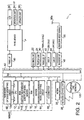
- the panel board P is connected to the main board M via the panel I/F 46.
- the panel board P is a board that controls the operation panel CP having the operation unit 34, LCD 36 and the speaker unit 38, in accordance with commands issued by the main board M.
- the panel board P is categorized corresponding to the category of the operation panel CP (e.g., a group of the operation panels CP having the one-line indication LCD 36, a group of the operation panels CP having the two-line indication LCD 36).
- the panel board P1 there are four categories of panels P1-P4. In Fig. 1, the panel board P1 is shown.
- the panel board P includes a CPU 112 that controls the operation of respective parts (e.g., operation unit 34, LCD 36 and speaker unit 38) of the operation panel CP, a ROM 114 storing programs executed by the CPU 112 and fixed value data, a RAM 112 temporarily storing data/programs for procedures executed by the CPU 112, a panel board category identifying circuit 162 that identifies the category of the panel board P, a panel identifying circuit 164 that identifies the model of the operation panel CP, an AD converter 166 that carries out an AD (analog-to-digital) conversion to the voltage value output by the panel identifying circuit 164, and an input/output port 142.
- a CPU 112 that controls the operation of respective parts (e.g., operation unit 34, LCD 36 and speaker unit 38) of the operation panel CP
- a ROM 114 storing programs executed by the CPU 112 and fixed value data
- a RAM 112 temporarily storing data/programs for procedures executed by the CPU 112
- the ROM 114 includes a function table memory 114a.
- the function table memory 114a is configured to store a function table similar to the function table stored in the function table memory 14a of the main board M.
- the function table stored in the function table memory 114a contains functional information that is necessary to make a combination of the main board M with a panel board P function properly, for each model of the MFD 1.
- each part of the CP i.e., the operation unit 34, LCD 36 and speaker unit 38
- the operation unit 34 controlled by the panel board P includes a plurality of input keys (e.g., buttons and switches) to execute various functions of the MFD 1.
- the LCD 36 displays various pieces of information regarding the operation of the MFD 1.
- the speaker unit 38 includes a speaker and a driving circuit for the speaker.
- the panel board category identifying circuit 162 includes, at least, a DC power source unit (not shown), a third resistance unit (not shown) provided between the DC power source unit 112 and a port C 112a provided to the CPU 112, a fourth resistance unit (not shown) provided between the DC power source unit and a port D 112b provided to the CPU 112, and an earth unit (not shown).
- the output signals to the port C 112a and port D 112b of the panel board category identifying circuit 162 are set to ON (High) level or OFF (Low) level.
- the ON/OFF setting of the output signals to the port C 112a and port D 112d is determined when the panel board P is manufactured.
- predetermined combinations of ON/OFF signals are applied to the port C 112a and port D 112b, respectively. That is, four different combinations of ON/OFF signals applied to the ports C and D 112a, 112b correspond to the four categories P1-P4, respectively.
- the panel identifying circuit 164 is configured such that specific voltages corresponding to models of the operation panel CP are output.
- the panel identifying circuit 164 includes, at least, a DC power source unit (not shown), an earth unit (not shown), and a fixed resistance unit (not shown) and a variable resistance unit (not shown) provided, in series, between the earth unit and the DC power source unit.
- a voltage value is output to the AD converter 166.
- the voltage output to the AD converter 166 can be adjusted by changing the value of the variable resistance, and the voltage value is set for each model of the operation panel CP. Since different voltages are output the AD converter for respective models of operation panels CP, it becomes possible to determine the model of the operation panel CP based on the AD value of the voltage.
- the CPU 112 the ROM 114, the RAM 116, the AD converter 166 are connected to the input/output port 142, to which the operation unit 34, the LCD 36, the speaker unit 38 and the panel I/F 46 are also connected.
- Fig. 2 shows a block diagram of the MFD 1 in which a main board M2 is employed as the main board M.
- the MFD 1 shown in Fig. 2 (i.e., the main board M1) has circuits realizing a cordless function.
- the main board M2 includes a main body I/F 48, which is connected to the ASIC 52, in addition to the configuration of the MFD 1 shown in Fig. 1.
- the main body I/F 48 is an interface to which a base main body board 50 provided with an antenna 50a is connected. By use of the antenna 50a, a wireless communication with an external cordless (wireless) handset (not shown) is realized.
- the configuration of the panel board P is omitted for brevity, and it may have the structure similar to that shown in Fig. 1.
- main board M2 shown in Fig. 2 and the main board M1 shown in Fig. 1 are of different categories, it is possible to identify the category based on the combination of the ON/OFF states of the signals output from the main board category identifying circuit 62 to the port A 12a and port B 12b of the CPU 12.
- FIGs. 3A and 3B are plan views of operation panels of different models.
- Fig. 3A shows an operation panel CPa
- Fig. 3B shows an operation panel CPb.
- the operation panel CP (CPa or CPb) has a variety of keys 34a-34g constituting the operation unit 34, and the LCD 36.
- the speaker unit 38 is also included in the operation panel CP (CPa or CPb), however, in Figs. 3A and 3B, it is omitted for brevity.
- the input key 34a is a power button. If the key 34a is depressed when the MFD 1 is powered OFF, the power is supplied to the MFD 1, while if the key 34a is depressed when the MFD 1 is powered ON, the MFD 1 is powered OFF.
- the input key 34b is an arrow key and also functions as a menu set key, which enables a user to select a function or a setting value from among a list displayed on the LCD 36.
- the input key 34c is a mode selection key with which the user can select one of the operable functions (e.g., a facsimile function, a copier function, a scanner function, a media print function, etc.).
- operable functions e.g., a facsimile function, a copier function, a scanner function, a media print function, etc.
- the input keys 34d are ten keys, which are used to input a telephone number of a destination station when the MFD 1 operates in the FAX mode and/or to input setting values.
- the input keys 34e are setting buttons, which are pressed to instruct specific functions in respective operation modes (e.g., the on-hook dialing function in the FAX mode).
- the input key 34f is a stop button that instructs the system to stop a current operation if the button is depressed during the operation in one of respective operation modes.
- the input keys 34g are start buttons, which are operated to start the operation of each function in the FAX mode and COPY mode.
- the LCD 36 displays a variety of pieces of information related to the MFD 1.
- setting values are displayed when various setting in a function setting operation is performed. Further, when the MFD 1 is in a standby state, current settings may be displayed on the LCD 36 as standby information.
- the operation panels CPa and CPb are different in arrangement of the input keys 34a-34g, and have different types of LCD 36.
- the operation panel CPa is configured such that the input key 34a is provided on the right-hand side end portion of the operation panel CPa, and the input key 34b is arranged on the left-hand side of the input key 34a.
- the input keys 34g are arranged below the input key 34b in Fig. 3A, and the input key 34f is located on the left-hand side of the input keys 34g.
- the input key 34c enabling selection of four modes.
- the input keys 34d are arranged on the left-hand side of the input key 34c and the LCD 36 located above the input key 34c.
- input keys 34e are arranged on the left-hand side of the input keys 34d.
- the LCD 36 on the operation panel CPa is a single-line display type LCD.
- the operation panel CPb is configured such that the input keys 34g are provided on the right-hand side end portion of the operation panel CPb. Above the input keys 34g, in Fig. 3B, the input key 34f is provided. On the left-hand side of the input keys 34g, the input key 34b is provided, and below the input key 34b, in Fig. 3B, part of input keys 34e are provided. At a lower central portion of the operation panel CPb, the input keys 34c for selecting three modes are arranged. On the left-hand side of the input keys 34c and the LCD 36 located above the input keys 34c, the input keys 34d are arranged. On the left-hand side of the input keys 34d, the remaining part of the input keys 34e are provided, and above the input keys 34e, the input key 34a is provided.
- the LCD 36 of the operation panel CPb is a two-line display type LCD.
- a function table corresponding to the type of the CP is retrieved from the function table memories 14a and 114a, as will be described with reference to flowcharts shown in Figs. 7-9.
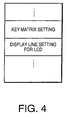
- Fig. 4 schematically shows an example of a function table stored in the function table memories 14b and 114b.
- a model of the MFD 1 is determined.
- one function table is defmed.
- the function table stores settings of the key matrix, the number of lines of the LCD and the like, which are the settings for enabling the operation panel CP corresponding to the function table to function correctly.
- the function table is selected corresponding to a model, which is determined in the main procedure, which is shown in Fig. 7, executed by the main board M.
- the function table corresponding to the operation panel CP suitable for the model of the MFD 1 is selected, even if the MFD 1 has a variety of models, the common control program can be used, and the operation panel CP functions properly.
- FIG. 5A shows a relationship between the combination of outputs of the main board category identifying circuit 62 and types of main board M (i.e., main boards M1-M4).
- the main board M1 which is the main board M of a first category (see Fig. 1), is configured such that the main board category identifying circuit 62 outputs signals representing OFF and OFF to the port A 12a and port B 12b of the CPU 12, respectively. Therefore, in the procedure shown in Fig. 7, if the OFF and OFF states are detected at the port A 12a and port B 12b, the category of the main board M is determined to be the main board M1 (see Fig. 1).
- the category of the main board M is determined to be the main board M2 (see Fig. 2). If OFF and ON states are detected at the port A 12a and port B 12b of the CPU 12, the category of the main board M is determined to be the main board M3. If ON and ON states are detected at the port A 12a and port B 12b of the CPU 12, the category of the main board M is determined to be the main board M4. As above, and as indicate in Fig. 5A based on the combination of the ON/OFF states of the two ports 12a and 12b connected to the main board category identifying circuit 62, the category of the main board (i.e., one of the main board M1 through main board M4) is identified.
- Fig. 5B shows a relationship between the main boards M1-M4 of the four categories, which are identified based on the output signals of the main board category identifying circuit 62, AD converted values of the voltage output by the model identifying circuit 64, and models of the MFD 1.
- the model of the MFD 1 is identified.
- a range of the AD converted values of the voltages output by the model identifying circuit 64 is from 0 to 3FF. According to the first embodiment, the range from 0 to 3FF is divided in to 16 steps. Therefore, based on the states of the signals output by the main board category identifying circuit 62 and the AD value of the voltage output by the mode identifying circuit 64, 64 models (i.e., model 1 to model 64) can be identified. Since the AD value of the voltage output by the model identifying circuit 64 is used, the voltage output by the model identifying circuit 64 can be detected at a relatively high resolution. Accordingly, the identification of the model can also be made at high accuracy.
- Fig. 5C shows a combination of the main board M and the operation panel CP (i.e., the panel board P) for each of the 16 models.
- the combinations for models 16-64 are omitted.
- each of model 1 to model 16 employs the main board M1.
- the main boards M1 and operation panel CP i.e., panel board P
- the main board M1 is used as the main board M
- panel 18 is used as the operation panel CP.
- the panel 18 is, as is shown in Fig. 6B, a panel board P whose category is panel board P2, which will be described later.
- FIG. 6A shows a relationship between four categories (panel boards P1-P4) of the panel board P and outputs of the panel board category identifying circuit 162.
- the panel board category identifying circuit 162 when the panel board P is the first category panel board P1 (see Fig. 1), the panel board category identifying circuit 162 outputs OFF signals to port C 112a and port D 112b of the CPU 112. Therefore, as illustrated in a flowchart shown in Fig. 9, when the OFF states are detected at port C 112a and port D 112b, the category of the panel board P is identified as the panel board P1 (see Fig. 1).
- the category of the panel board P is determined as the panel board P2 (not shown).
- the category of the panel board P is determined as the panel board P3 (not shown).
- the category of the panel board P4 is determined as the panel board P4 (not shown).
- the four categories of the panel board P (i.e., panel boards P1-P4) can be distinguished.
- Fig. 6A shows a relationship between the four categories of the panel board P (i.e., panel boards P1-P4) identified based on the states of the output signals of the panel board category identifying circuit 162, the AD converted values of the voltages output by the panel identifying circuit 164, and the operation panels PC of the MFD 1.
- the category of the panel board P i.e., panel boards P1-P4
- the model of the operation panel determined based on the AC value output by the panel identifying circuit 164.
- the range of the AD converted values of the voltages output by the panel identifying circuit 164 is from 0 to 3FF, and in this embodiment, the range is divided into 16 steps. Therefore, in the embodiment, based on the states of the output signals of the panel board category identifying circuit 162, and AD converted value of the voltage output by the panel identifying circuit 164, 64 models of operation panels PC (i.e., panel 1- panel 64) can be distinguished. Further, by referring to the AD converted values of the voltage output by the panel identifying circuit 164, the voltage output by the panel identifying circuit 164, the voltage output by the panel identifying circuit 164 can be detected at a high resolution, thereby identifying the model of the operation panel CP with a high accuracy.
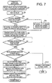
- Fig. 7 is a flowchart illustrating a main procedure executed on the main board M of the MFD 1 according to the first embodiment.
- the main procedure starts when the MFD 1 is powered ON as the input key 34a is operated.
- the procedure shown in Fig. 7 is stored as a part of programs in the ROM 14.
- control detects the ON/OFF states of the port A 12a and port B 12b, and identifies the category of the main board M (S1). Then, control reads the value output by the AD converted 66 (S2). In S3, control judges whether the model is identified based on the category of the main board M identified in S 1 and the AD value obtained in S2. If the model is identified (S3: YES), control sets the model of the MFD 1 as the identified model (S4).
- control sets the mode of the MFD 1 as a model that has the largest production number, which is stored in the substitution model memory 14b (S5).
- control After execution of S4 or S5, control transmits the operation panel model identifying signal and model information indicative of the identified model to the panel board P (S6), and judges whether information indicating the model of the operation panel CP (hereinafter, referred to as operation panel model information) is input through the panel board P (S7).
- control transmits an operation panel model identification instructing signal is transmitted to the panel board P.
- an operation panel model identifying procedure (Fig. 9), which will be described later, is executed.
- the model of the operation panel CP is identified, and operation panel model information related to the identified operation panel CP is transmitted to the main board M.
- control judges whether the operation panel model information is received. If the operation panel model information has not been received from the panel board P (S7: NO), control waits for the reception of the operation panel model information from the panel board P. If the operation panel model information is received (S7: YES), control judges whether the model of the MFD 1 identified in S4 or S5 corresponds to the operation panel CP indicated by the operation panel model information received form the panel board P (S8). For example, if the model identified in S4 or S5 is the model 8, and the operation panel CP indicated by the operation pane model information is the panel 51, control determines that both correspond to each other (see Fig. 5C).
- control selects the function table corresponding to the identified model of the MFD 1 from the function table memory 14a (S9), and carries our the initialization in accordance with the selected function table (S10). After execution of S10, control transmits function table information indicative of the selected function table to the panel board P (S11), and then the main board M operates in a standby state.
- control transmits an error signal to the panel board P (S12), and finishes the main procedure.
- an error procedure is executed by the panel board P (see Fig. 8), and an error state is notified through the LCD 36 and/or speaker unit 38 of the operation panel CP.
- the user is notified of the occurrence of the error condition. Accordingly, the user can deal with the error condition immediately by re-setting the main board M and/or the panel board P, or ask a manufacture of the MFD 1 to fix the error condition.
- Fig. 8 shows a flowchart illustrating a reception procedure to be executed by the panel board P.
- the reception procedure is started when the panel board P receives a signal or information from the main board M.
- control identifies what is represented by the signal or information received from the main board M. If the signal or information received from the main board M is the operation panel model identification instructing signal and model information, which are received as a result of execution ofS6 at the main board, control proceeds to S22. In this case, control executes the operation panel model identifying procedure, which will be described later, to identify the model of the operation panel CP. Then, control finishes the reception procedure.
- control selects, in accordance with the received function table information, a function table corresponding to the model identified in the main procedure (see Fig. 7) executed by the main board M from the function table memory 114a (S23), and carries out the initial setting of the operation panel CP in accordance with the thus selected function table (S24).
- a key matrix corresponding to the arrangement of the operation unit 34 of the operation panel CP in accordance with the key matrix setting of the function table, and in accordance with the setting of the line number of the LCD, a display setting of the LCD 36 is carried out. After execution of S24, control finishes the reception procedure.
- the signal or information received from the main board M is the error signal which is received as a result of execution of S 12 by the main board M (S21: ERROR SIGNAL), an error notifying operation such as an error display on the LCD 36, an alarm by the speaker unit 38 to notify the user of the error condition is executed (S25).
- control carries out a procedure corresponding to the received signal or information (S26) and finishes the reception procedure.
- control detects the ON/OFF states of the port C 112a and port D 112b to identify the category of the panel board P (S41). then, in S42, control obtains the value output by the AD converter 166. After execution of S42, control judges whether a model of the operation panel CP can be identified based on the category of the panel board P identified in S41 and the AD converted value obtained in S42 (S43). If the model of the operation panel CP can be identified (S43: YES), control sets the model of the operation panel CP to the mode thereof identified from the category of the panel board P identified in S41 and the AD converted value obtained in S42 (S44).
- control sets the model of the operation panel CP corresponding to the model of the MFD 1 input to the panel board P as a result of execution of S6 in the main procedure executed by the main board M as the model of the operation panel CP (S45).
- control After execution of S44 or S45, control transmits the model of the operation panel CP identified in S44 or S45 to the main board M (S46). Then, by the main board M, S8 of the main procedure (see Fig. 7) is executed. After execution of S46, control finishes the panel model identifying operation.
- substitute model memory 14b as the substitute model, one having the largest production number among the models corresponding to each model of the operation panels CP is stored as well as the model having the largest production number of all the models.
- Fig. 10 shows a flowchart of the main procedure executed by the main board M, according to the second embodiment.
- the procedure shown in Fig. 10 is stored as a part of programs executed by the main board M and stored in the ROM 14.
- steps S1-S3 are executed, which are similar to those of the first embodiment. If, in S3, the model of the MFD 1 is identified (S3: YES), S4 and S6 are executed similarly to the first embodiment. If the model is not identified (S3: NO), control skips S4, and proceeds to S6.
- control refers to the substitute model memory 14b, and sets the model of the MFD 1 as the model of the MFD having the largest production number among the model corresponding to the identified operation panel CP (S63). After execution of S63, control proceeds to S64. As S63 is executed, even if the model of the MFD 1 has not been identified in S3, if the operation panel CP is identified in the panel model identifying procedure (Fig. 11), which will be described later, the model of the MFD 1 can be identified based on the identified operation panel CP.
- the model having the largest production number is set as the model of the MFD 1, possibility that the basic functions do not work at all can be reduced. If at least the basic functions are available, re-setting thereafter can be carried out relatively easily.
- control skips S63, and proceeds to S64. In this case, control proceeds with the model of the MFD 1 and the model of the operation panel CP being unidentified.
- control judges whether both the model of the MFD 1 and model of the operation panel CP have been identified. If both the model of the MFD 1 and model of the operation panel CP have been identified (S64: YES), control judges whether the operation panel CP corresponding to the model of the MFD 1 identified in S4 or S63 corresponds to the operation panel CP indicated by the operation panel information received from the panel board P (S65).
- control executes S9-S 11 similarly to the first embodiment, and proceeds to operate in the standby state.
- control sets the model having the largest production number stored in the substitute model memory 14b as the model of the MFD 1 (S66), and proceeds to S9. Since the model having the largest production number is set as the model of the MFD 1 if at least one of the model of the MFD 1 or the model of the operation panel CP, a possibility that the basic functions do not work can be reduced. If the basic functions are available, a troublesome re-setting work can be made easier.
- control executes S9 similarly to the first embodiment, and finishes the main procedure.
- Fig. 11 shows a flowchart illustrating a panel model identifying procedure executed by the panel board P according to the second embodiment.
- the procedure is stored as a part of control program executed by the panel board P and stored in the ROM 114.
- control judges whether the model of the MFD 1 is identified in the model information which is input together with the operation panel model identification instruction from the main board M (S81). If the model of the MFD 1 has been identified (S81: YES), control sets the model of the operation panel CP to the operation panel CP corresponding to the model of the MFD 1 (S82). After execution of S82, control proceeds to S46.
- the function table corresponding to the identified model of the MFD 1 is obtained and set.
- the main board M and the panel board P are identified based on the hardware configuration, and the function table enabling the operation panel CP to operate correctly is selected and set. According to such an MFD, a variety of models can be controlled with a single program, which suppresses the manufacturing cost of the variety of MFDs.
- the AD converted values of the voltages output by the model identifying circuit and the panel identifying circuit are referred to. Since the AD converted values are used, a lot of models of MFDs and operation panels can be distinguished from each other.
- the model of the MFD is identified based on the output state of the main board category identifying circuit 62 and the AD converted value of the voltage output by the model identifying circuit 66.
- the operation panel CP is identified based on the output states of the panel board category identifying circuit 162 and the AD converted value of the voltage output by the panel identifying circuit 164. Further, when the operation panel corresponding to the identified model of the MFD and the operation panel as identified coincide with each other, the function table corresponding to the identified model is retrieved and set.
- the identification of the operation panel CP based on the output states of the panel board category identifying circuit 162 and the AD converted value of the voltage output by the panel identifying circuit 164 may be omitted, and a function table corresponding to the model of the MFD 1 identified in accordance with the output states of the main board category identifying circuit 62 and the AD value of the output by the model identifying circuit 64, and the thus obtained table may be set.
- the panel board category identifying circuit 162 and the panel identifying circuit 164 may not be provided on the panel board P, which reduces the manufacturing cost.
- the category of the main board M is determined based on the ON/OFF signals applied to the port A 12a and port B 12b from the main board category identifying circuit 62. This may be modified such that more than two signals respectively representing the ON/OFF state are applied from the main board category identifying circuit 62 to corresponding number of ports provided to the CPU 112. According to such a configuration, the number of distinguishable categories increases, and therefore, the number of identifiable models of the MFD 1 can be increased.
- the panel board category identifying circuit 16 may be configured to output more than two ON/OFF signals and the CPU 112 may be configured to have the corresponding number of ports to detect more than two ON/OFF signals, respectively.
- the CPU 112 of the panel board P identifies the model of the operation panel CP based on the outputs of the panel board category identifying circuit 162 and the panel identifying circuit 164.
- This configuration may be modified such that the outputs of the panel board category identifying circuit 162 and the panel identifying circuit 164 are input to predetermined ports of the CPU 12 of the main board M, and the operation panel CP may be identified while the main procedure of the main board M (see Fig. 7 or 10) is being executed.
- the main board M need not be limited to the main board M1 (see Fig. 1) but one of main boards M2-M4 can also be used.
- the panel board P need not be limited to the panel board P1, but can be replaced with one of the panel boards P2-P4. The same applies to the configuration shown in Fig. 2.
- the model of the MFD 1 is identified based on the model of the operation panel as identified. That is, in such a case, steps S61-S63 of Fig. 10 are executed.
- steps S61-S63 may be omitted and the model having the largest production number of all the MFDs may be selected as the model of the MFD 1 if neither the model of the MFD 1 nor the operation panel board has been identified.
- S61-S63 may be omitted, and an error signal may be transmitted to the panel board P if neither the model of the MFD 1 nor the operation panel board has been identified.
Landscapes
- Engineering & Computer Science (AREA)
- Multimedia (AREA)
- Signal Processing (AREA)
- Human Computer Interaction (AREA)
- Facsimiles In General (AREA)
- Stored Programmes (AREA)
- Accessory Devices And Overall Control Thereof (AREA)
- Control Or Security For Electrophotography (AREA)
Applications Claiming Priority (1)
| Application Number | Priority Date | Filing Date | Title |
|---|---|---|---|
| JP2004218757A JP4293083B2 (ja) | 2004-07-27 | 2004-07-27 | 多機能周辺装置 |
Publications (2)
| Publication Number | Publication Date |
|---|---|
| EP1622352A1 true EP1622352A1 (de) | 2006-02-01 |
| EP1622352B1 EP1622352B1 (de) | 2010-04-21 |
Family
ID=35262037
Family Applications (1)
| Application Number | Title | Priority Date | Filing Date |
|---|---|---|---|
| EP05254661A Ceased EP1622352B1 (de) | 2004-07-27 | 2005-07-27 | Mehrfach-Funktions-Gerät |
Country Status (5)
| Country | Link |
|---|---|
| US (1) | US7694028B2 (de) |
| EP (1) | EP1622352B1 (de) |
| JP (1) | JP4293083B2 (de) |
| CN (1) | CN1728757B (de) |
| DE (1) | DE602005020719D1 (de) |
Families Citing this family (8)
| Publication number | Priority date | Publication date | Assignee | Title |
|---|---|---|---|---|
| CN102119508B (zh) * | 2008-06-10 | 2015-04-08 | 惠普开发有限公司 | 将交换机层级结构后面的多功能设备呈现为单功能设备 |
| JP5241374B2 (ja) * | 2008-08-07 | 2013-07-17 | キヤノン株式会社 | 配信装置、配信方法、及びコンピュータプログラム |
| JP5298795B2 (ja) * | 2008-11-18 | 2013-09-25 | 富士ゼロックス株式会社 | 画像形成装置 |
| KR20130084092A (ko) * | 2012-01-16 | 2013-07-24 | 삼성전자주식회사 | 화상형성장치 |
| JP6953927B2 (ja) * | 2016-10-27 | 2021-10-27 | 株式会社リコー | 情報処理装置、情報処理方法、情報処理プログラム及び操作装置 |
| CN207766616U (zh) * | 2017-12-04 | 2018-08-24 | 欧普照明股份有限公司 | 产品类别识别系统及照明灯具 |
| JP7251313B2 (ja) * | 2019-05-24 | 2023-04-04 | セイコーエプソン株式会社 | 画像読取装置 |
| CN111322821A (zh) * | 2020-02-21 | 2020-06-23 | 海信容声(广东)冰箱有限公司 | 一种冰箱及其控制板机型的识别方法 |
Citations (6)
| Publication number | Priority date | Publication date | Assignee | Title |
|---|---|---|---|---|
| US5610725A (en) * | 1993-06-25 | 1997-03-11 | Ricoh Company, Ltd. | Communication system for managing data of resources of image forming unit |
| JPH10311984A (ja) | 1997-05-13 | 1998-11-24 | Seiko Epson Corp | 液晶表示パネル、液晶表示装置、液晶表示パネルの検査方法および液晶表示装置の製造方法 |
| EP0917006A2 (de) * | 1997-11-17 | 1999-05-19 | Xerox Corporation | Ein-/Ausgabe-Modell für Benutzeroberflächen mit mehreren Funktionen |
| US6204928B1 (en) * | 1995-10-11 | 2001-03-20 | Canon Kabushiki Kaisha | Data processing apparatus and a method for controlling the apparatus |
| US20030044185A1 (en) * | 2001-08-27 | 2003-03-06 | Hisanori Kawaura | Image forming apparatus, program updating method and recording medium |
| EP1292102A2 (de) * | 2001-08-27 | 2003-03-12 | Ricoh Company, Ltd. | Bilderzeugungsgerät, Verfahren zum Aktualisieren von Programmen und Informationsaufzeichnungsmedium |
Family Cites Families (5)
| Publication number | Priority date | Publication date | Assignee | Title |
|---|---|---|---|---|
| US6298421B1 (en) * | 1998-01-12 | 2001-10-02 | Brother Kogyo Kabushiki Kaisha | Data storage device |
| US6633931B2 (en) * | 2000-12-29 | 2003-10-14 | Hewlett-Packard Development Company, L.P. | Card identification system and method for an input/output interface |
| JP4279538B2 (ja) * | 2002-10-30 | 2009-06-17 | 富士ゼロックス株式会社 | 機器設定方法、機器設定システム、情報処理装置及びコンピュータプログラム |
| US20040207864A1 (en) * | 2003-04-18 | 2004-10-21 | Combs Steven Donald | Method for operating a printer and method for operating a printer controller |
| US20060070055A1 (en) * | 2004-09-24 | 2006-03-30 | Hodder Leonard B | Method of updating printer firmware and printing device employing the method |
-
2004
- 2004-07-27 JP JP2004218757A patent/JP4293083B2/ja not_active Expired - Lifetime
-
2005
- 2005-07-26 US US11/188,848 patent/US7694028B2/en active Active
- 2005-07-27 EP EP05254661A patent/EP1622352B1/de not_active Ceased
- 2005-07-27 DE DE602005020719T patent/DE602005020719D1/de not_active Expired - Lifetime
- 2005-07-27 CN CN2005100876276A patent/CN1728757B/zh not_active Expired - Fee Related
Patent Citations (6)
| Publication number | Priority date | Publication date | Assignee | Title |
|---|---|---|---|---|
| US5610725A (en) * | 1993-06-25 | 1997-03-11 | Ricoh Company, Ltd. | Communication system for managing data of resources of image forming unit |
| US6204928B1 (en) * | 1995-10-11 | 2001-03-20 | Canon Kabushiki Kaisha | Data processing apparatus and a method for controlling the apparatus |
| JPH10311984A (ja) | 1997-05-13 | 1998-11-24 | Seiko Epson Corp | 液晶表示パネル、液晶表示装置、液晶表示パネルの検査方法および液晶表示装置の製造方法 |
| EP0917006A2 (de) * | 1997-11-17 | 1999-05-19 | Xerox Corporation | Ein-/Ausgabe-Modell für Benutzeroberflächen mit mehreren Funktionen |
| US20030044185A1 (en) * | 2001-08-27 | 2003-03-06 | Hisanori Kawaura | Image forming apparatus, program updating method and recording medium |
| EP1292102A2 (de) * | 2001-08-27 | 2003-03-12 | Ricoh Company, Ltd. | Bilderzeugungsgerät, Verfahren zum Aktualisieren von Programmen und Informationsaufzeichnungsmedium |
Also Published As
| Publication number | Publication date |
|---|---|
| US7694028B2 (en) | 2010-04-06 |
| JP2006041909A (ja) | 2006-02-09 |
| DE602005020719D1 (de) | 2010-06-02 |
| JP4293083B2 (ja) | 2009-07-08 |
| CN1728757A (zh) | 2006-02-01 |
| US20060026306A1 (en) | 2006-02-02 |
| EP1622352B1 (de) | 2010-04-21 |
| CN1728757B (zh) | 2010-08-25 |
Similar Documents
| Publication | Publication Date | Title |
|---|---|---|
| JP5219431B2 (ja) | 無線通信システム及びその制御方法、画像入出力装置及びその制御方法、並びにプログラム | |
| US8289131B2 (en) | Security method and system using touch screen | |
| EP1777936B1 (de) | Multifunktionales Peripheriegerät | |
| JPH1098566A (ja) | 画像入出力システム及びスキャナ装置と画像形成装置とを備えた多機能周辺装置 | |
| EP1622352B1 (de) | Mehrfach-Funktions-Gerät | |
| US7721249B2 (en) | User interface apparatus, processing apparatus, user interface method, program for implementing the method, and storage medium storing the program | |
| CN100371175C (zh) | 控制图像传感器操作的方法 | |
| JP5500883B2 (ja) | 画像読取装置及びその制御方法とそのプログラム | |
| CN100473099C (zh) | 传真机 | |
| KR20020089744A (ko) | 팩스 데이터의 선택적 인쇄가 가능한 팩시밀리 겸용프린터 및 팩스 데이터의 선택적 인쇄방법 | |
| JP3689617B2 (ja) | 画像形成システム及びその制御方法及び記憶媒体 | |
| KR101324178B1 (ko) | 화상형성장치 및 화상형성장치의 제어방법 | |
| WO2005027507A1 (ja) | 画像処理装置、画像形成装置、及び画像処理方法 | |
| JP2002366287A (ja) | 無線インタフェース接続操作パネル | |
| JP4787144B2 (ja) | 表示制御装置および表示制御システム | |
| JP7655100B2 (ja) | 通信装置及びプログラム | |
| JP7243387B2 (ja) | 情報処理装置、情報処理方法及び情報処理プログラム | |
| JP7293806B2 (ja) | 情報処理装置、情報処理方法及び情報処理プログラム | |
| KR100472431B1 (ko) | 이중 원고 이송 검출 방법 | |
| JP2008186251A (ja) | 画像形成装置、プリントシステム、プリント枚数計数方法およびプリント枚数計数プログラム | |
| EP1928164B1 (de) | Faksimilegerät | |
| JP2018098544A (ja) | 画像形成装置、制御方法およびプログラム | |
| JP6568397B2 (ja) | 画像形成装置及びそれを含むシステム | |
| JP2024047174A (ja) | 画像処理装置、制御方法およびプログラム | |
| JP4062099B2 (ja) | 操作端末装置 |
Legal Events
| Date | Code | Title | Description |
|---|---|---|---|
| PUAI | Public reference made under article 153(3) epc to a published international application that has entered the european phase |
Free format text: ORIGINAL CODE: 0009012 |
|
| AK | Designated contracting states |
Kind code of ref document: A1 Designated state(s): AT BE BG CH CY CZ DE DK EE ES FI FR GB GR HU IE IS IT LI LT LU LV MC NL PL PT RO SE SI SK TR |
|
| AX | Request for extension of the european patent |
Extension state: AL BA HR MK YU |
|
| 17P | Request for examination filed |
Effective date: 20060725 |
|
| 17Q | First examination report despatched |
Effective date: 20060824 |
|
| AKX | Designation fees paid |
Designated state(s): DE FR GB |
|
| GRAP | Despatch of communication of intention to grant a patent |
Free format text: ORIGINAL CODE: EPIDOSNIGR1 |
|
| GRAS | Grant fee paid |
Free format text: ORIGINAL CODE: EPIDOSNIGR3 |
|
| GRAA | (expected) grant |
Free format text: ORIGINAL CODE: 0009210 |
|
| AK | Designated contracting states |
Kind code of ref document: B1 Designated state(s): DE FR GB |
|
| REG | Reference to a national code |
Ref country code: GB Ref legal event code: FG4D |
|
| REF | Corresponds to: |
Ref document number: 602005020719 Country of ref document: DE Date of ref document: 20100602 Kind code of ref document: P |
|
| PLBE | No opposition filed within time limit |
Free format text: ORIGINAL CODE: 0009261 |
|
| STAA | Information on the status of an ep patent application or granted ep patent |
Free format text: STATUS: NO OPPOSITION FILED WITHIN TIME LIMIT |
|
| 26N | No opposition filed |
Effective date: 20110124 |
|
| REG | Reference to a national code |
Ref country code: FR Ref legal event code: PLFP Year of fee payment: 12 |
|
| REG | Reference to a national code |
Ref country code: FR Ref legal event code: PLFP Year of fee payment: 13 |
|
| REG | Reference to a national code |
Ref country code: FR Ref legal event code: PLFP Year of fee payment: 14 |
|
| PGFP | Annual fee paid to national office [announced via postgrant information from national office to epo] |
Ref country code: FR Payment date: 20180620 Year of fee payment: 14 |
|
| PGFP | Annual fee paid to national office [announced via postgrant information from national office to epo] |
Ref country code: GB Payment date: 20180625 Year of fee payment: 14 |
|
| GBPC | Gb: european patent ceased through non-payment of renewal fee |
Effective date: 20190727 |
|
| PG25 | Lapsed in a contracting state [announced via postgrant information from national office to epo] |
Ref country code: GB Free format text: LAPSE BECAUSE OF NON-PAYMENT OF DUE FEES Effective date: 20190727 |
|
| PG25 | Lapsed in a contracting state [announced via postgrant information from national office to epo] |
Ref country code: FR Free format text: LAPSE BECAUSE OF NON-PAYMENT OF DUE FEES Effective date: 20190731 |
|
| PGFP | Annual fee paid to national office [announced via postgrant information from national office to epo] |
Ref country code: DE Payment date: 20220615 Year of fee payment: 18 |
|
| REG | Reference to a national code |
Ref country code: DE Ref legal event code: R119 Ref document number: 602005020719 Country of ref document: DE |
|
| PG25 | Lapsed in a contracting state [announced via postgrant information from national office to epo] |
Ref country code: DE Free format text: LAPSE BECAUSE OF NON-PAYMENT OF DUE FEES Effective date: 20240201 |