EP1624491B1 - Festkörperbildsensor mit elektronischer Kontrolle der Apertur - Google Patents
Festkörperbildsensor mit elektronischer Kontrolle der Apertur Download PDFInfo
- Publication number
- EP1624491B1 EP1624491B1 EP04405490A EP04405490A EP1624491B1 EP 1624491 B1 EP1624491 B1 EP 1624491B1 EP 04405490 A EP04405490 A EP 04405490A EP 04405490 A EP04405490 A EP 04405490A EP 1624491 B1 EP1624491 B1 EP 1624491B1
- Authority
- EP
- European Patent Office
- Prior art keywords
- electrodes
- photosensor
- charge
- charge carriers
- potential
- Prior art date
- Legal status (The legal status is an assumption and is not a legal conclusion. Google has not performed a legal analysis and makes no representation as to the accuracy of the status listed.)
- Expired - Lifetime
Links
Images


Classifications
-
- H—ELECTRICITY
- H10—SEMICONDUCTOR DEVICES; ELECTRIC SOLID-STATE DEVICES NOT OTHERWISE PROVIDED FOR
- H10F—INORGANIC SEMICONDUCTOR DEVICES SENSITIVE TO INFRARED RADIATION, LIGHT, ELECTROMAGNETIC RADIATION OF SHORTER WAVELENGTH OR CORPUSCULAR RADIATION
- H10F30/00—Individual radiation-sensitive semiconductor devices in which radiation controls the flow of current through the devices, e.g. photodetectors
- H10F30/20—Individual radiation-sensitive semiconductor devices in which radiation controls the flow of current through the devices, e.g. photodetectors the devices having potential barriers, e.g. phototransistors
- H10F30/21—Individual radiation-sensitive semiconductor devices in which radiation controls the flow of current through the devices, e.g. photodetectors the devices having potential barriers, e.g. phototransistors the devices being sensitive to infrared, visible or ultraviolet radiation
- H10F30/28—Individual radiation-sensitive semiconductor devices in which radiation controls the flow of current through the devices, e.g. photodetectors the devices having potential barriers, e.g. phototransistors the devices being sensitive to infrared, visible or ultraviolet radiation the devices being characterised by field-effect operation, e.g. junction field-effect phototransistors
- H10F30/2823—Individual radiation-sensitive semiconductor devices in which radiation controls the flow of current through the devices, e.g. photodetectors the devices having potential barriers, e.g. phototransistors the devices being sensitive to infrared, visible or ultraviolet radiation the devices being characterised by field-effect operation, e.g. junction field-effect phototransistors the devices being conductor-insulator-semiconductor devices, e.g. diodes or charge-coupled devices [CCD]
-
- H—ELECTRICITY
- H10—SEMICONDUCTOR DEVICES; ELECTRIC SOLID-STATE DEVICES NOT OTHERWISE PROVIDED FOR
- H10F—INORGANIC SEMICONDUCTOR DEVICES SENSITIVE TO INFRARED RADIATION, LIGHT, ELECTROMAGNETIC RADIATION OF SHORTER WAVELENGTH OR CORPUSCULAR RADIATION
- H10F39/00—Integrated devices, or assemblies of multiple devices, comprising at least one element covered by group H10F30/00, e.g. radiation detectors comprising photodiode arrays
- H10F39/10—Integrated devices
- H10F39/12—Image sensors
-
- H—ELECTRICITY
- H10—SEMICONDUCTOR DEVICES; ELECTRIC SOLID-STATE DEVICES NOT OTHERWISE PROVIDED FOR
- H10F—INORGANIC SEMICONDUCTOR DEVICES SENSITIVE TO INFRARED RADIATION, LIGHT, ELECTROMAGNETIC RADIATION OF SHORTER WAVELENGTH OR CORPUSCULAR RADIATION
- H10F39/00—Integrated devices, or assemblies of multiple devices, comprising at least one element covered by group H10F30/00, e.g. radiation detectors comprising photodiode arrays
- H10F39/10—Integrated devices
- H10F39/12—Image sensors
- H10F39/15—Charge-coupled device [CCD] image sensors
Definitions
- the present invention relates to all sensing and measuring techniques that require electrical control over the effective photosensitive area in a solid-state device that is sensitive to quasi-static or temporally modulated electromagnetic wavefields, preferably in the ultraviolet, visible or infrared spectral range.
- quasi-statically this capability is required for the dynamic control of the sensitivity of the photosensor, to replace or enhance the function of a shutter. In this way, the dynamic range of the photosensor is improved and can be adapted to the lighting conditions in a scene.
- the present invention relates specifically to all of these sensing and measurement techniques that require dense one- or two-dimensional arrays of pixels with electronic aperture control.
- the mechanical shutter For a long time, the traditional means of adapting the limited dynamic range of a film or an optoelectronic image sensor to the widely varying lighting conditions in a scene has been the mechanical shutter.
- a mechanical shutter one can control the effectively deposited amount of incident radiation on the photosensitive area by selecting different exposure times, during which the shutter is open, while it is closed for the rest of the time.
- the effective fraction of detected to incident radiation is therefore determined by the duty cycle of the pulse-width modulation of the incident light through the mechanical shutter function.
- An electronic shutter function that is equivalent to a mechanical shutter function can be obtained with interline-transfer charge-coupled devices (IT-CCD), as described by A.J.P. Theu Giveaway in “Solid-state imaging with charge-coupled devices", Kluwer, Dordrecht, 1995.
- the exposure time is started with an electrical reset operation, which clears the storage site from all previously accumulated photocharges.
- incident light is converted into photocharges, and these photocharges are accumulated.
- the exposure time is ended by transporting the accumulated photocharges under an optically shielded storage area.
- the effective fraction of detected to incident radiation is determined by the duty cycle of the pulse-width modulation of the incident light through the electronic shutter function. For this reason, the switching action is binary (on-off), and neither an electrically controllable optical attenuator nor the demodulation/mixing with a continuously varying time-function is possible.
- U.S. Patents Nos. 6,667,768 and 6,556,244 describe alternative electronic shutters in image sensors that can be purely realized with industry-standard complementary metal-oxide-semiconductor (CMOS) technology.
- CMOS complementary metal-oxide-semiconductor
- a proportional number of photocharges as a function of incident radiation energy is generated in photodiodes, and these photocharges are stored in capacitors, under the control of transistors that either electrically connect the capacitors to the photodiodes, or disconnect the electrical path between capacitors and photodiodes.
- the switching action is binary (on-off), and neither an electrically controllable optical attenuator nor a demodulation/mixing with a continuously varying time-function is possible.
- U.S. Patent No. 5,856,667 teaches the use of CCD photodetection, switching and storage devices for the binary demodulation/mixing with a binary time-function exhibiting low noise performance, in particular for applications in optical time-of-flight range imaging.
- the switching action is binary (on-off), and neither an electrically controllable optical attenuator nor a demodulation/mixing with a continuously varying time-function is possible.
- variable optical attenuators acting on a complete image at a time such as the one described in U.S. Patent No. 6,665,485 , employ an additional attenuating element, usually placed between the imaging lens and the surface of the image sensor. Examples include varying optical density (gradient) filters, or liquid-crystal-based attenuator elements. None of these electrically controllable optical attenuators can be implemented monolithically in the image sensor itself.
- the two major disadvantages of this technique are on one hand the charge or voltage noise contributed by the channels of the multiplying transistors, and on the other hand the low operation frequency of the mixing action that is limited to a few 10 kHz, because the transistors are operated in sub-threshold where their high effective resistance leads to a low-pass RC filter action with low cutoff frequency.
- WO-2004/001354 describes an optoelectronic sensing device for the local demodulation of a modulated electromagnetic wavefield.
- the device consists of a resistive, transparent electrode on top of an insulator layer that is produced over a semiconducting substrate whose surface is electrically kept in depletion.
- the electrode is connected with two or more contacts to a number of clock voltages that are operated synchronously with the frequency of the modulated wavefield.
- a lateral electric field is created that separates and transports photogenerated charge pairs in the semiconductor to respective diffusions close to the contacts.
- the lateral electric field is acting in one direction only.
- the device By repetitively storing and accumulating photocharges in the diffusions, electrical signals are generated that are subsequently read out for the determination of local phase shift, amplitude and offset of the modulated wavefield.
- the device does not provide any electrically controllable optical attenuator.
- a principle object of the invention is to provide an optoelectronic sensing device for electromagnetic radiation whose effective photosensitive aperture can be changed electrically.
- a second object of the invention is to provide an optoelectronic sensing device for the local mixing or demodulation of a modulated electromagnetic wavefield, preferably in the ultraviolet, the visible and the near infrared portion of the electromagnetic spectrum, using a continuously varying mixing or demodulation time-function.
- a further object of invention is to provide an architecture for a geometrical arrangement of the sensing device in one or two dimensions for the realization of line and image sensors with adaptable electronic aperture control and for the realization of line and image sensors capable of mixing or demodulating incident wavefields.
- the present invention is achieved with a multitude of transparent electrodes on top of a transparent insulating layer placed on a semiconductor substrate.
- Photogenerated charge carriers move laterally under the influence of the voltage distribution on the various electrodes, and they are collected at the two ends of the photosensor in diffusions or in MOS structures.
- the voltage distribution on the electrodes is such that the voltage at the two outermost electrodes is maximum (if photoelectrons are collected), the voltage is minimum at an interior electrode, and monotonously decreasing in between.
- the lateral position of the electrode with minimum voltage defines the effective photosensitive area of the photosensor.
- a lateral electric drift field is generated at the semiconductor surface, which drift field reverses its direction along at least one straight line in the plane surface.
- the potential of the drift field is non-monotonic and has a global extremity, i.e., a global minimum or maximum, in the interior of the active region of the photosensor.
- the photosensor according to the invention is formed in a semiconductor substrate with a plane surface. It comprises an active region for converting incident radiation into charge carriers of a first and a second charge type, separating the charge carriers of the first charge type from the charge carriers of the second charge type and accumulating charge carriers of at least one charge type.
- the active region has field-generating means for generating a lateral electric drift field at the semiconductor surface in the active region.
- the field-generating means comprise an insulator layer formed on the semiconductor substrate and at least three conductive electrodes. Each electrode has a contact for applying an electric potential to the electrode.
- the electrodes are arranged above the insulator layer such that a row of at least three electrodes is formed along at least one straight line in the plane surface.
- the method according to the invention for sensing incident radiation, modulated with a modulation frequency comprises the steps of:
- the drift field reverses its direction along at least one straight line in the plane surface.
- the photosensor according to the invention When used in a quasi-static way, the photosensor according to the invention is capable of dynamic exposure control. If the position is modulated sinusoidally from left to right at the frequency of incident modulated light, this incident light can be demodulated or mixed with very little non-harmonic distortions. Because of the compact nature of this photosensor with electronic aperture control, it can be used as picture element in image sensors with a large number of such pixels, either for dynamic exposure control, for optoelectronic mixing or for demodulation, such as required in optical time-of-flight range cameras.
- the photosensor with electronic aperture control according to the invention overcomes the disadvantages of the prior art in several respects.
- the effective geometric aperture of all pixels of an image detector can be changed with electrical signals, directly on the pixel level in the semiconductor domain, without resorting to electromechanical or optoelectronic shutters.
- the photosensor according to the invention makes it possible to employ a continuous mixing or demodulation time-function.
- the photosensor is simple to fabricate by employing standard CCD or CMOS process technology.
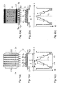
- a first embodiment of the photosensor according to the invention is shown in Figure 1(a) in a top view and in Figure 1(b) in a cross section.
- the photosensor makes use of a substrate S made of a semiconductor material such as silicon for the conversion of incident photons into electron-hole pairs.
- this semiconductor substrate material is p-doped, and that we want to detect photoelectrons as minority charge carriers in the semiconductor material. All subsequent arguments can be suitably modified to hold true for the detection of photogenerated holes as minority carriers in n-doped semiconductor material.
- the semiconductor substrate S is covered with a preferably transparent insulator layer O, preferably an oxide, as available in industry standard CMOS processes.
- the thickness of the insulator layer O may vary between 1 nm and 1 ⁇ m. Thinner insulator layers O let a larger part of electric surface fields pass through into the semiconductor substrate S, but these thinner oxide layers O are more difficult to fabricate.
- On top of the insulator layer O a multitude of preferably transparent, conductive electrode strips E 1 , ... E i , ... E n (n ⁇ 3) are arranged, as employed for example for the fabrication of charge-coupled devices (CCD).
- the preferred electrode material is poly-crystalline silicon, but any transparent conductive oxide (TCO), such as indium tin oxide (ITO) or zinc oxide (ZnO), or even metal can be used.
- TCO transparent conductive oxide
- ITO indium tin oxide
- ZnO zinc oxide
- the insulator material and the electrode material should be transparent for the incident radiation In, and/or it should have openings so that the incident radiation In can be transmitted into the bulk of the semiconductor substrate S. It is also possible to thin the semiconductor substrate S to a thickness of several micrometers, and to let the radiation impinge from the back of the device, as in so-called back-illuminated photosensors.
- n + diffusion volume D1, D2 is arranged, which can be preset to a given reference potential and to which an electronic charge-detection circuit (not shown) is connected.
- the potential distribution ⁇ (x) should preferably have the following properties for the detection of photoelectrons:
- the charge-dividing line L divides the straight line given by the coordinate x (or the straight line Ib-Ib in Fig. 1(a) ) in the plane surface of the substrate S into a first section A1 of length w and a second section A2 of length (a - w).
- the first and second sections A1, A2 are immediately adjacent to each other. In both sections A1, A2, the drift field is directed towards the dividing line L or is zero. Thus, the drift field reverses its direction along the straight line x.
- the exemplified potential distribution ⁇ (x) of Figure 1(c) has the form of a bi-directional staircase with equal steps.
- Incident electromagnetic radiation In is transmitted through the electrode strips E 1 -E n and the covering insulator layer O.
- the incident radiation In creates photoelectrons (represent by points in Fig. 1(c) ) in the bulk of the semiconductor substrate S. These photoelectrons are transported laterally either by electric field drift in areas where the potential ⁇ (x) varies as a function of distance, or the transport mechanism is diffusion in field-free regions in which the potential ⁇ (x) is constant.
- the effective photosensitive area of the photosensor can be changed accordingly.
- the diffusion wells D1, D2 have about the same length as the electrode strips E 1 -E n in the embodiment of Fig. 1(a) , their capacitance could become quite substantial. In some cases, it is desirable to collect the charge carriers in diffusion wells that have a small capacitance. Therefore, an alternative embodiment of the present invention is realized as illustrated in Figure 2 .
- the electrode strips E 1 -E n are short, leading to a form factor that is close to square.
- the length of the diffusion wells D1, D2 is also short, so that the diffusion wells D1, D2 have a correspondingly small capacitance.
- the active region In order to collect the charge carriers over a larger area, the active region is extended accordingly. Since it is necessary to transport the photoelectrons to the electrode-strip region without losing their lateral position, the transport mechanism employed must be drift in an electric field that is perpendicular to the electrode-strip arrangement.
- a resistive electrode surface H on top of a large zone of the insulator layer O consisting of a transparent, resistive material with an electrical sheet resistivity that surpasses 10 ⁇ / ⁇ , and preferably is more than 10 k ⁇ / ⁇ , e.g., many tens of k ⁇ / ⁇ , and up to about 1 M ⁇ / ⁇ .
- a preferred material for the realization of this resistive electrode H is poly-crystalline silicon.
- the resistive electrode H is contacted at its two edges with two contacts C1, C2 running along the width of the photosensor, and which are connected to a static or switchable voltage source.
- the voltage at the contact C2 close to the electrode strips E 1 -E n must be lower than their potential minimum, so that photocharges move from under this contact C2 to the electrode-strip zone.
- the voltage at the other contact C1 must be lower than the voltage at the first contact C2, leading to a current flow from the first contact C2 to the second contact C1, leading in turn to a linearly changing potential distribution perpendicular to the contacts C1, C2. This causes the desired linearly changing potential distribution at the semiconductor-insulator interface, due to which the photoelectrons move from their generation site in a perpendicular fashion to the electrode-strip zone.
- the photogenerated charges collected by one diffusion well D1 represent the fraction of total photocharges corresponding to the ratio "distance from the diffusion well to the electrode with minimum potential" w divided by "total width of the insulator region" a (cf. Fig. 1 ).
- the effective photosensitive area of the photosensor can be changed accordingly, irrespective of the length a of the total photosensitve area.
- Both embodiments discussed up to here lead to lateral potential distributions ⁇ (x) that are staircase-like. Since electric field drift is a faster charge transport mechanism than diffusion, it is desirable to employ a realization offering non-zero electric fields in the complete photosensitive (or active) area. This can be achieved with the photosensor illustrated in Figure 3 . It comprises a resistive electrode surface H on top of the insulator O, made of a transparent, highly resistive material with an electrical sheet resistivity that surpasses 10 ⁇ / ⁇ , and preferably is more than 10 k ⁇ / ⁇ , e.g., many tens of k ⁇ / ⁇ , and up to about 1 M ⁇ / ⁇ .
- a series of short contact electrodes E 1 -E n with small contact areas is fabricated in a straight line on each of the two edges of the resistive electrode H. If a pattern of voltage values is applied to the contact electrodes E 1 -E n , the resulting potential distribution ⁇ (x) at the semiconductor surface varies linearly between two contact electrodes E 1 -E n .
- the potential distribution ⁇ (x) linearly interpolates between the potential values beneath the contact electrodes E 1 -E n . As long as all voltages are different, the piecewise linear potential distribution ⁇ (x) has the desired effect of non-zero electric field and highspeed photoelectron transport in the complete photosensitive area.
- the position of the effective dividing line L for the photocharge separation i.e., the width of the effective w photosensitive area
- the position of the effective dividing line L for the photocharge separation is not limited to this number n and the respective discrete positions. It can rather be chosen arbitrarily by applying suitable analog voltage patterns to the electrodes E 1 -E n .
- This is illustrated in Figures 4 and 5 , showing two cases of voltage distributions for the photosensor structure of Fig. 3 .
- a selected electrode E 3 of the electrodes E 1 -E 4 is supplied with a minimum voltage, and the adjacent electrodes E 2 , E 4 to the left and to the right have an identical, higher voltage.
- the dividing line L for the photocharge separation is at the center of the selected electrode E 3 .
- two adjacent electrodes E 2 , E 3 are supplied with the same voltage, and their respective neighbors E 1 , E 4 to the left and to the right have an identical, higher voltage.
- the effective photocharge dividing line L is found to lie in the middle between the two electrodes E 2 , E 3 with minimum voltage. In the general case of arbitrary voltage distributions, it is possible, therefore, to realize any desired position of the photocharge dividing line L, i.e., any width w of the effective photosensitive area.
- the mixing or demodulation capability of the photosensor according to the invention can be exploited, for example, for the optical measurement of the three-dimensional shape of an object according to the time-of-flight ranging technique, as described in R. Lange and P. Seitz, "Solid-State Time-of-Flight Range Camera", IEEE J. Quantum Electronics, Vol. 37 (3), 390-397, 1 March 2001 .
- An object is illuminated with a modulated source of light, and the reflected light is imaged with an optical imaging lens on a two-dimensional detection and demodulation device according to the invention.
- the present invention allows to measure all modulation parameters of the incident modulated wavefield, in particular the local phase delay ⁇ in the following way.
- the position w(t) of the photocharge dividing line L in a photosensor is modulated with a periodic signal that has the same frequency as the modulated source of light.
- Preferred periodic signals are harmonic, rectangular or triangular functions of the time.
- the photogenerated charges Q1 and Q3 are collected in the two diffusion wells D1, D2 of the photosensor over one or many periods.
- a second photosensor which is illuminated with the same reflected modulated radiation r(t), has the same modulation of the dividing line w(t) as the first photosensor, but it is 90 degrees out of phase.
- Another possibility is to replace the second photosensitive photosensor with a second measurement by the first photosensitive photosensor, after the measurement values Q1 and Q3 have been stored.
- This assumes that the reflected modulated radiation r(t) does not change its modulation parameters during the complete exposure time required for the acquisition of Q1, Q2, Q3 and Q4.
- the depletion region in the semiconductor substrate S extends deeply into the semiconductor bulk, to depths of several tens of micrometers.
- vertical electric fields extend deeply into the semiconductor S, leading to fast and efficient drift transport of photogenerated charges also for longer wavelengths of the incident photons.
- the photosensor according to the invention can be arranged in a one- or two-dimensional arrangement, for the creation of line or image sensors with electronic aperture control.
- This is illustrated in Figure 6 for the example of an image sensor making use of a conventional active-pixel-sensor (APS) readout circuit.
- Each of the two diffusion wells D1, D2 for the accumulation of photocharges is connected to a charge-detection circuit, such as the illustrated source-follower circuit.
- each diffusion well D1, D2 is connected to the gate of a source-follower transistor SF.
- the source-follower transistor SF is in series with a row-select transistor RT, which is connected to a signal column SC that terminates in a load resistor or a current source.
- the diffusion well is reset to a reference voltage on a reference-voltage line V using a pixel-reset transistor PR.
- all pixel-reset transistors PR in a row are switched at the same time under the control of a row-reset signal on a row-reset-signal line RR.
- All row-select transistors RT in a row are switched at the same time under the control of a row-select signal on a row-select-signal line RS.
- the electrodes E i of all pixels in a column are electrically connected, and they are preferably realized as electrode strips having the length of the column. If the different columns should be controlled individually, each set of electrodes needs its own connections to the outside world.
- the corresponding column electrodes E i of all columns can be connected to the same control-signal line e i .
- the number of connections to the outside world is the same as the number of electrode strips E i in one column.
Landscapes
- Solid State Image Pick-Up Elements (AREA)
Claims (17)
- Photosensor, der in einem Halbleitersubstrat (S) mit einer ebenen Oberfläche gebildet ist, wobei der Photosensor umfasst:eine aktive Region eines Pixels zum:Umwandeln einer einfallenden Strahlung (In) in Ladungsträger einer ersten und zweiten Ladungsart,Trennen der Ladungsträger der ersten Ladungsart von den Ladungsträgern der zweiten Ladungsart; undAkkumulieren von Ladungsträgern mindestens einer Ladungsart,wobei die aktive Region Felderzeugungsmittel (0, E1-En) zum Erzeugen eines lateralen elektrischen Driftfeldes an der Halbleiteroberfläche in der aktiven Region aufweist,wobei das Felderzeugungsmittel umfasst:eine strahlungsdurchlässige Isolierschicht (O), die auf dem Halbleitersubstrat (S) gebildet ist,wobeidas Felderzeugungsmittel (O, E1-En) Folgendes umfasst:mindestens drei leitende und strahlungsdurchlässige Elektroden (E1-En),wobei jede Elektrode (E1-En) einen Kontakt zum Anlegen eines elektrischen Potenzials an die Elektrode (E1-En) aufweist,die Elektroden (E1-En) über der Isolierschicht (O) derart angeordnet sind, dass eine Reihe von mindestens drei Elektroden (E1-En) entlang mindestens einer geraden Linie in der ebenen Oberfläche gebildet ist,dadurch gekennzeichnet, dassmindestens eine Elektrode (Ei) zwischen den äußersten Elektroden (E1, En) einem globalen Potenzialminimum einer lateralen Potenzialverteilung (Φ) ausgesetzt ist,die Elektroden (Ei-E1, Ei-E1) zwischen dem globalen Minimum und den äußersten Elektroden einem erhöhten Potenzial ausgesetzt sind, so dass Spannungen von dem globalen Minimum monoton auf das jeweilige höchste Potenzial an den äußeren Elektroden (E1, En) ansteigen, unddie Potenzialverteilung (Φ) veränderbar ist, wodurch die Änderung der Größe der effektiven lichtempfindlichen Fläche des Pixels möglich ist.
- Photosensor nach Anspruch 1, wobei die Elektroden (E1-En) parallele Streifen sind, wobei sich jeder Streifen über die gesamte Länge der aktiven Region in einer Dimension der ebenen Oberfläche erstreckt.
- Photosensor nach Anspruch 1, wobei die Elektroden (E1-En) nur in einer ersten Zone der aktiven Region angeordnet sind und eine zweite Zone der aktiven Region, die neben der ersten Zone liegt, mit zweiten Felderzeugungsmitteln (0, H, C1, C2) zum Erzeugen eines zweiten lateralen elektrischen Driftfeldes an der Halbleiteroberfläche in der zweiten Zone bereitgestellt ist, wobei das zweite laterale elektrische Driftfeld zum Transportieren der Ladungsträger mindestens einer Ladungsart zu der ersten Zone geeignet ist.
- Photosensor nach einem der vorangehenden Ansprüche, wobei eine widerstandsfähige Schicht (H) zwischen der Isolierschicht (O) und den Elektroden (E1-En) angeordnet ist.
- Photosensor nach Anspruch 4, wobei die widerstandsfähige Schicht (H) einen Flächenwiderstand von mehr als 10 Ω/□ aufweist, und vorzugsweise mehr als 10 Ω/ Φ, z.B. mehre zehn kΩ/□ und bis zu etwa 1 MΩ/□.
- Photosensor nach einem der vorangehenden Ansprüche, wobei die Isolierschicht (O), die Elektroden (E1-En) und, falls vorhanden, die widerstandsfähige Schicht (H) für die einfallende Strahlung (In) transparent sind.
- Photosensor nach Anspruch 5 oder 6, wobei die Elektroden (E1-En) Polysilizium, ein transparentes leitendes Oxid, wie Indiumzinnoxid oder Zinkoxid, oder Metall umfassen.
- Photosensor nach einem der vorangehenden Ansprüche, wobei das Halbleitersubstrat (S) ein Siliziumsubstrat ist und vorzugsweise ein p-dotiertes Siliziumsubstrat.
- Photosensor nach einem der vorangehenden Ansprüche, wobei die Isolierschicht (O) eine Oxidschicht ist, z.B. eine Siliziumdioxidschicht, und eine Dicke zwischen 1 nm und 1000 nm aufweist.
- Photosensor nach einem der vorangehenden Ansprüche, wobei eine Diffusionswanne (D1, D2) oder ein Integrationsgate zum Akkumulieren von Ladungsträgern nahe mindestens einer der äußersten Elektroden (E1, En) der Reihe von mindestens drei Elektroden (E1, En) bereitgestellt ist.
- Photosensor nach einem der vorangehenden Ansprüche, des Weiteren umfassend eine elektronische Schaltung zum Auslesen der akkumulierten Ladungsträger, z.B. eine Ladungsintegrationsschaltung oder eine Aktiv-Pixel-Sensor-Schaltung.
- Photosensor nach einem der vorangehenden Ansprüche, wobei der Photosensor mit einem CMOS- oder einem CCD-Prozess hergestellt wurde.
- Bildsensor, umfassend mehrere Pixel, die in einer ein- oder zweidimensionalen Gruppe angeordnet sind, dadurch gekennzeichnet, dass die Pixel Photosensoren nach einem der vorangehenden Ansprüche sind.
- Bildsensor nach Anspruch 13, wobei die Elektroden (E1-En) parallele Streifen sind, wobei sich jeder Streifen über eine vollständige Spalte des Bildsensors erstreckt.
- Verfahren zum Erfassen einfallender Strahlung (In), umfassend die folgenden Schritte:Umwandeln der einfallenden Strahlung (In) in Ladungsträger einer ersten und einer zweiten Ladungsart in einer aktiven Region eines Photosensors, der in einem Halbleitersubstrat (S) mit einer ebenen Oberfläche gebildet ist,Erzeugen eines lateralen elektrischen Driftfeldes an der Halbleiteroberfläche in der aktiven Region, Trennen der Ladungsträger der ersten Ladungsart von den Ladungsträgern der zweiten Ladungsart mit Hilfe des Driftfeldes, undAkkumulieren von Ladungsträgern mindestens einer Ladungsart, dadurch gekennzeichnet, dass das Driftfeld seine Richtung entlang mindestens einer geraden Linie (x) in der ebenen Oberfläche umkehrt,wobei mindestens drei leitende Elektroden (E1-En), die von dem Halbleitersubstrat (S) isoliert sind, in der aktiven Region bereitgestellt sind, jede Elektrode mit einem Kontakt zum Anlegen eines elektrischen Potenzials an die Elektrode bereitgestellt ist und die Potenziale an die Kontakte angelegt werden,wobei das Driftfeld durch Anlegen von mindestens drei Potenzialen an die aktive Region erzeugt wird, wobei mindestens zwei der mindestens drei Potenziale voneinander unterschiedlich sind, undwobei die mindestens drei Potenziale die folgenden Eigenschaften aufweisen: (a) ein globales Potenzialminimum wird an einen oder mehrere benachbarte Kontakte (Ei) angelegt; (b) an jeder Seite des Potenzialminimums erhöhen sich die Potenziale monoton zu dem Kontakt der äußersten Elektrode (E1, En); (c) Potenziale, die an die äußersten Kontakte (E1, En) angelegt sind, sind geringer als Potenziale, die an Stellen (D1, D2) zum Akkumulieren von Ladungsträgern neben den äußersten Elektroden (E1, En) angelegt werden; (d) alle Potenziale, die an die Kontakte angelegt werden, sind höher als das Potenzial, bei dem das Halbleitersubstrat (S) gehalten wird.
- Verfahren nach Anspruch 15, wobei die gerade Linie (x) in einen ersten Abschnitt (A1) und einen zweiten Abschnitt (A2), die nebeneinander liegen, geteilt (L) ist, wobei in dem ersten Abschnitt (A1) das Driftfeld in eine erste Richtung (+x) gerichtet oder Null ist, und in dem zweiten Abschnitt (A2) das Driftfeld in eine zweite, entgegen gesetzte Richtung (-x) gerichtet oder Null ist.
- Verfahren nach Anspruch 16, wobei die Längen (w, a - w) des ersten (A1) und zweiten (S2) Abschnitts mit der Zeit geändert werden.
Priority Applications (4)
| Application Number | Priority Date | Filing Date | Title |
|---|---|---|---|
| DE602004021251T DE602004021251D1 (de) | 2004-08-04 | 2004-08-04 | Festkörperbildsensor mit elektronischer Kontrolle der Apertur |
| EP04405490A EP1624491B1 (de) | 2004-08-04 | 2004-08-04 | Festkörperbildsensor mit elektronischer Kontrolle der Apertur |
| PCT/CH2005/000445 WO2006012764A1 (en) | 2004-08-04 | 2005-07-27 | Solid-state photosensor with electronic aperture control |
| US11/659,313 US8436401B2 (en) | 2004-08-04 | 2005-07-27 | Solid-state photosensor with electronic aperture control |
Applications Claiming Priority (1)
| Application Number | Priority Date | Filing Date | Title |
|---|---|---|---|
| EP04405490A EP1624491B1 (de) | 2004-08-04 | 2004-08-04 | Festkörperbildsensor mit elektronischer Kontrolle der Apertur |
Publications (2)
| Publication Number | Publication Date |
|---|---|
| EP1624491A1 EP1624491A1 (de) | 2006-02-08 |
| EP1624491B1 true EP1624491B1 (de) | 2009-05-27 |
Family
ID=34932228
Family Applications (1)
| Application Number | Title | Priority Date | Filing Date |
|---|---|---|---|
| EP04405490A Expired - Lifetime EP1624491B1 (de) | 2004-08-04 | 2004-08-04 | Festkörperbildsensor mit elektronischer Kontrolle der Apertur |
Country Status (4)
| Country | Link |
|---|---|
| US (1) | US8436401B2 (de) |
| EP (1) | EP1624491B1 (de) |
| DE (1) | DE602004021251D1 (de) |
| WO (1) | WO2006012764A1 (de) |
Families Citing this family (16)
| Publication number | Priority date | Publication date | Assignee | Title |
|---|---|---|---|---|
| EP1624490B1 (de) * | 2004-08-04 | 2018-10-03 | Heptagon Micro Optics Pte. Ltd. | Grossflächiger Pixel für die Verwendung in einem Bildsensor |
| GB2446429A (en) | 2006-12-08 | 2008-08-13 | E2V Tech | Photosensor with variable sensing area |
| GB0803702D0 (en) | 2008-02-28 | 2008-04-09 | Isis Innovation | Transparent conducting oxides |
| DE102009001159A1 (de) * | 2009-02-25 | 2010-09-02 | Johann Wolfgang Goethe-Universität Frankfurt am Main | Elektrooptische Kamera mit demodulierendem Detektorarray |
| KR101623960B1 (ko) | 2009-06-04 | 2016-05-25 | 삼성전자주식회사 | 광전자 셔터, 이의 동작 방법 및 광전자 셔터를 채용한 광학 장치 |
| GB0915376D0 (en) | 2009-09-03 | 2009-10-07 | Isis Innovation | Transparent conducting oxides |
| US8464952B2 (en) * | 2009-11-18 | 2013-06-18 | Hand Held Products, Inc. | Optical reader having improved back-illuminated image sensor |
| FR2961347B1 (fr) * | 2010-06-15 | 2012-08-24 | E2V Semiconductors | Capteur d'image a multiplication d'electrons |
| ITUD20110149A1 (it) * | 2011-09-29 | 2013-03-30 | Monica Vatteroni | Dispositivo fotorilevatore per sensori elettro-ottici a dinamica di luce variabile |
| TWI465979B (zh) * | 2012-04-16 | 2014-12-21 | Au Optronics Corp | 觸控面板 |
| EP2867923B1 (de) | 2012-06-27 | 2020-01-15 | Teledyne Dalsa B.V. | Bildsensor und vorrichtung mit solch einem bildsensor |
| US9191637B2 (en) * | 2013-09-10 | 2015-11-17 | Kabushiki Kaisha Toshiba | Solid-state imaging apparatus |
| EP3193190B1 (de) * | 2016-01-15 | 2023-04-12 | Sony Depthsensing Solutions N.V. | Detektorvorrichtung mit majoritätsstrom und schaltung zur steuerung des stroms |
| CN109814083B (zh) * | 2018-11-14 | 2024-06-14 | 光微信息科技(合肥)有限公司 | 电流辅助光子解调型像素单元、背照式图像传感器芯片、成像系统、形成方法和测算方法 |
| CN112864183B (zh) * | 2021-01-18 | 2023-08-25 | 上海集成电路装备材料产业创新中心有限公司 | 一种改善传输迟滞的像元结构 |
| JP2026054829A (ja) * | 2024-09-17 | 2026-03-30 | 浜松ホトニクス株式会社 | 固体撮像装置 |
Family Cites Families (18)
| Publication number | Priority date | Publication date | Assignee | Title |
|---|---|---|---|---|
| US4481522A (en) * | 1982-03-24 | 1984-11-06 | Rca Corporation | CCD Imagers with substrates having drift field |
| US4994405A (en) * | 1989-11-21 | 1991-02-19 | Eastman Kodak Company | Area image sensor with transparent electrodes |
| JPH06140442A (ja) * | 1992-10-29 | 1994-05-20 | Matsushita Electric Ind Co Ltd | 電荷転送装置 |
| DE4440613C1 (de) | 1994-11-14 | 1996-07-25 | Leica Ag | Vorrichtung und Verfahren zur Detektion und Demodulation eines intensitätsmodulierten Strahlungsfeldes |
| US5591996A (en) * | 1995-03-24 | 1997-01-07 | Analog Devices, Inc. | Recirculating charge transfer magnetic field sensor |
| SE509569C2 (sv) | 1995-10-26 | 1999-02-08 | Hoernell International Ab | Vätskekristallslutarkonstruktion |
| JP4060365B2 (ja) * | 1996-09-05 | 2008-03-12 | ルドルフ シュヴァルト | 電磁波の位相情報および/または振幅情報を調べるための方法と装置 |
| KR100246358B1 (ko) | 1997-09-25 | 2000-03-15 | 김영환 | 전자셔터를 구비한 액티브 픽셀 센서 |
| US6667768B1 (en) | 1998-02-17 | 2003-12-23 | Micron Technology, Inc. | Photodiode-type pixel for global electronic shutter and reduced lag |
| DE10035135B4 (de) | 2000-07-19 | 2010-02-18 | Sick Ag | Verfahren und Vorrichtung zur Entfernungsmessung |
| US7352454B2 (en) * | 2000-11-09 | 2008-04-01 | Canesta, Inc. | Methods and devices for improved charge management for three-dimensional and color sensing |
| US6906793B2 (en) * | 2000-12-11 | 2005-06-14 | Canesta, Inc. | Methods and devices for charge management for three-dimensional sensing |
| KR20030003699A (ko) * | 2001-01-23 | 2003-01-10 | 코닌클리즈케 필립스 일렉트로닉스 엔.브이. | 전하 결합 소자 및 전하 결합 소자 제조 방법 |
| TW530951U (en) | 2001-05-30 | 2003-05-01 | Hon Hai Prec Ind Co Ltd | Manual tunable optical attenuator |
| GB2389960A (en) * | 2002-06-20 | 2003-12-24 | Suisse Electronique Microtech | Four-tap demodulation pixel |
| DE10228103A1 (de) | 2002-06-24 | 2004-01-15 | Bayer Cropscience Ag | Fungizide Wirkstoffkombinationen |
| EP1458087B1 (de) * | 2003-03-10 | 2005-10-12 | CSEM Centre Suisse d'Electronique et de Microtechnique SA | Elektrische Schaltung, Verfahren und Vorrichtung zur Demodulation eines intensitätsmodulierten Signals |
| JP4391145B2 (ja) * | 2003-06-27 | 2009-12-24 | 富士フイルム株式会社 | 固体撮像装置 |
-
2004
- 2004-08-04 EP EP04405490A patent/EP1624491B1/de not_active Expired - Lifetime
- 2004-08-04 DE DE602004021251T patent/DE602004021251D1/de not_active Expired - Lifetime
-
2005
- 2005-07-27 US US11/659,313 patent/US8436401B2/en not_active Expired - Fee Related
- 2005-07-27 WO PCT/CH2005/000445 patent/WO2006012764A1/en not_active Ceased
Also Published As
| Publication number | Publication date |
|---|---|
| US20090026508A1 (en) | 2009-01-29 |
| DE602004021251D1 (de) | 2009-07-09 |
| WO2006012764A1 (en) | 2006-02-09 |
| US8436401B2 (en) | 2013-05-07 |
| EP1624491A1 (de) | 2006-02-08 |
Similar Documents
| Publication | Publication Date | Title |
|---|---|---|
| EP1624490B1 (de) | Grossflächiger Pixel für die Verwendung in einem Bildsensor | |
| US8436401B2 (en) | Solid-state photosensor with electronic aperture control | |
| US8299504B2 (en) | Image sensing device and method of | |
| US8106472B2 (en) | Image sensor with large-area, high-sensitivity and high-speed pixels | |
| EP2284897B1 (de) | Demodulationspixel umfassender Majoritätsträgerstrom, eingegrabener Kanal und Hoch-Niedrig-Verbindung | |
| US6710370B2 (en) | Image sensor with performance enhancing structures | |
| US7622704B2 (en) | Optoelectronic detector with multiple readout nodes and its use thereof | |
| EP2863437B1 (de) | Festkörperbilderfassungsvorrichtung | |
| US11264521B2 (en) | Photosensitive field-effect transistor | |
| US8071410B2 (en) | Multi spectral sensor | |
| WO2018018026A1 (en) | Quantum film pixels with low readout noise | |
| TWI715538B (zh) | 背面入射型固體攝像裝置 | |
| KR20050023321A (ko) | 이미지 센싱 디바이스 및 그 방법 | |
| EP1909075A2 (de) | Fotosensor mit räumlicher Korrelation | |
| JPS63250171A (ja) | 密着型イメ−ジセンサ |
Legal Events
| Date | Code | Title | Description |
|---|---|---|---|
| PUAI | Public reference made under article 153(3) epc to a published international application that has entered the european phase |
Free format text: ORIGINAL CODE: 0009012 |
|
| AK | Designated contracting states |
Kind code of ref document: A1 Designated state(s): AT BE BG CH CY CZ DE DK EE ES FI FR GB GR HU IE IT LI LU MC NL PL PT RO SE SI SK TR |
|
| AX | Request for extension of the european patent |
Extension state: AL HR LT LV MK |
|
| 17P | Request for examination filed |
Effective date: 20060520 |
|
| AKX | Designation fees paid |
Designated state(s): CH DE FR GB LI |
|
| 17Q | First examination report despatched |
Effective date: 20080520 |
|
| GRAP | Despatch of communication of intention to grant a patent |
Free format text: ORIGINAL CODE: EPIDOSNIGR1 |
|
| RAP1 | Party data changed (applicant data changed or rights of an application transferred) |
Owner name: CSEM CENTRE SUISSE D'ELECTRONIQUE ET DE MICROTECHN |
|
| GRAS | Grant fee paid |
Free format text: ORIGINAL CODE: EPIDOSNIGR3 |
|
| GRAA | (expected) grant |
Free format text: ORIGINAL CODE: 0009210 |
|
| AK | Designated contracting states |
Kind code of ref document: B1 Designated state(s): CH DE FR GB LI |
|
| REG | Reference to a national code |
Ref country code: GB Ref legal event code: FG4D |
|
| REG | Reference to a national code |
Ref country code: CH Ref legal event code: EP |
|
| REF | Corresponds to: |
Ref document number: 602004021251 Country of ref document: DE Date of ref document: 20090709 Kind code of ref document: P |
|
| REG | Reference to a national code |
Ref country code: CH Ref legal event code: NV Representative=s name: SCHNEIDER FELDMANN AG PATENT- UND MARKENANWAELTE |
|
| PLBE | No opposition filed within time limit |
Free format text: ORIGINAL CODE: 0009261 |
|
| STAA | Information on the status of an ep patent application or granted ep patent |
Free format text: STATUS: NO OPPOSITION FILED WITHIN TIME LIMIT |
|
| 26N | No opposition filed |
Effective date: 20100302 |
|
| REG | Reference to a national code |
Ref country code: FR Ref legal event code: PLFP Year of fee payment: 12 |
|
| PGFP | Annual fee paid to national office [announced via postgrant information from national office to epo] |
Ref country code: CH Payment date: 20150820 Year of fee payment: 12 Ref country code: DE Payment date: 20150825 Year of fee payment: 12 Ref country code: GB Payment date: 20150827 Year of fee payment: 12 |
|
| PGFP | Annual fee paid to national office [announced via postgrant information from national office to epo] |
Ref country code: FR Payment date: 20150629 Year of fee payment: 12 |
|
| REG | Reference to a national code |
Ref country code: DE Ref legal event code: R119 Ref document number: 602004021251 Country of ref document: DE |
|
| REG | Reference to a national code |
Ref country code: CH Ref legal event code: PL |
|
| GBPC | Gb: european patent ceased through non-payment of renewal fee |
Effective date: 20160804 |
|
| PG25 | Lapsed in a contracting state [announced via postgrant information from national office to epo] |
Ref country code: LI Free format text: LAPSE BECAUSE OF NON-PAYMENT OF DUE FEES Effective date: 20160831 Ref country code: CH Free format text: LAPSE BECAUSE OF NON-PAYMENT OF DUE FEES Effective date: 20160831 |
|
| REG | Reference to a national code |
Ref country code: FR Ref legal event code: ST Effective date: 20170428 |
|
| PG25 | Lapsed in a contracting state [announced via postgrant information from national office to epo] |
Ref country code: FR Free format text: LAPSE BECAUSE OF NON-PAYMENT OF DUE FEES Effective date: 20160831 Ref country code: DE Free format text: LAPSE BECAUSE OF NON-PAYMENT OF DUE FEES Effective date: 20170301 Ref country code: GB Free format text: LAPSE BECAUSE OF NON-PAYMENT OF DUE FEES Effective date: 20160804 |