EP1624493A2 - Herstellungsverfahren eines optischen Moduls für Halbleiterbildaufnahmevorrichtung-Gehäuse - Google Patents
Herstellungsverfahren eines optischen Moduls für Halbleiterbildaufnahmevorrichtung-Gehäuse Download PDFInfo
- Publication number
- EP1624493A2 EP1624493A2 EP05106673A EP05106673A EP1624493A2 EP 1624493 A2 EP1624493 A2 EP 1624493A2 EP 05106673 A EP05106673 A EP 05106673A EP 05106673 A EP05106673 A EP 05106673A EP 1624493 A2 EP1624493 A2 EP 1624493A2
- Authority
- EP
- European Patent Office
- Prior art keywords
- lens
- diaphragm
- optical
- wafer
- module
- Prior art date
- Legal status (The legal status is an assumption and is not a legal conclusion. Google has not performed a legal analysis and makes no representation as to the accuracy of the status listed.)
- Withdrawn
Links
Images

Classifications
-
- H—ELECTRICITY
- H10—SEMICONDUCTOR DEVICES; ELECTRIC SOLID-STATE DEVICES NOT OTHERWISE PROVIDED FOR
- H10F—INORGANIC SEMICONDUCTOR DEVICES SENSITIVE TO INFRARED RADIATION, LIGHT, ELECTROMAGNETIC RADIATION OF SHORTER WAVELENGTH OR CORPUSCULAR RADIATION
- H10F77/00—Constructional details of devices covered by this subclass
- H10F77/50—Encapsulations or containers
-
- H—ELECTRICITY
- H10—SEMICONDUCTOR DEVICES; ELECTRIC SOLID-STATE DEVICES NOT OTHERWISE PROVIDED FOR
- H10F—INORGANIC SEMICONDUCTOR DEVICES SENSITIVE TO INFRARED RADIATION, LIGHT, ELECTROMAGNETIC RADIATION OF SHORTER WAVELENGTH OR CORPUSCULAR RADIATION
- H10F39/00—Integrated devices, or assemblies of multiple devices, comprising at least one element covered by group H10F30/00, e.g. radiation detectors comprising photodiode arrays
- H10F39/80—Constructional details of image sensors
- H10F39/804—Containers or encapsulations
-
- H—ELECTRICITY
- H10—SEMICONDUCTOR DEVICES; ELECTRIC SOLID-STATE DEVICES NOT OTHERWISE PROVIDED FOR
- H10F—INORGANIC SEMICONDUCTOR DEVICES SENSITIVE TO INFRARED RADIATION, LIGHT, ELECTROMAGNETIC RADIATION OF SHORTER WAVELENGTH OR CORPUSCULAR RADIATION
- H10F77/00—Constructional details of devices covered by this subclass
- H10F77/40—Optical elements or arrangements
-
- H—ELECTRICITY
- H10—SEMICONDUCTOR DEVICES; ELECTRIC SOLID-STATE DEVICES NOT OTHERWISE PROVIDED FOR
- H10F—INORGANIC SEMICONDUCTOR DEVICES SENSITIVE TO INFRARED RADIATION, LIGHT, ELECTROMAGNETIC RADIATION OF SHORTER WAVELENGTH OR CORPUSCULAR RADIATION
- H10F39/00—Integrated devices, or assemblies of multiple devices, comprising at least one element covered by group H10F30/00, e.g. radiation detectors comprising photodiode arrays
- H10F39/80—Constructional details of image sensors
- H10F39/806—Optical elements or arrangements associated with the image sensors
- H10F39/8063—Microlenses
Definitions
- the present invention relates to the field of optical sensors associated with semiconductor devices and, more particularly, to the manufacture of a semiconductor package with an optical sensor and in particular of the optical module thereof.
- optical module semiconductor packages are used, for example, for producing miniature cameras or imaging devices, for example in mobile telephones.
- Optical modules for optical sensor devices of semiconductor packages essentially consist of a hemispherical lens attached to a diaphragm placed at a focal distance of a microlens array made on an integrated circuit chip constituting the optical sensor.
- a first known family of optical modules consists of a rotatable plastic cover for suspending the lens and the diaphragm, and to be attached to the integrated circuit chip.
- the rotation of the cover serves, in particular, to adjust the focal length, therefore of Focus.
- This family of optical modules is generally intended for lenses made of plastic whose positioning and manufacturing tolerances (of the order of plus or minus 80 microns) are incompatible with the short focal length (a few millimeters) of this kind of lens. device.
- a second known family of optical modules consists of using a glass lens (generally hemispherical) reported on a diaphragm made on a glass spacer, itself based on the integrated circuit chip carrying the microsensors (phototransistors, microdiaphragms and microlenses).
- the present invention applies more particularly to this family of optical modules.
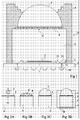
- FIG. 1 represents a conventional example of an optical sensor semiconductor package as described in the French patent application 03/12305 (03 / GR2 / 190) of the applicant.
- Such a housing 10 constituting a shooting element comprises an integrated circuit chip 1 constituting an optical sensor, on which have been represented hemispherical microlenses 2.
- these microlenses are integrated in the silicon of chip 1 above the phototransistors.
- the housing 10 also comprises a lens 3 disposed at a distance from the chip 1 and a diaphragm 4 against the lower face (facing the sensor) of the lens 3.
- a relatively thick glass spacer 6 (of the order of a few millimeters ) relative to the thickness of the chip 1, is interposed between the chip 1 and the diaphragm 4 and defines the focal length of the optical device.
- the assembly described above is made by batch in whole plates before being cut for individualization. The assembly then rests on a substrate 5.
- the electrical information provided by the integrated circuit chip 1 is reported, for example, from the upper surface of this chip carrying the microlenses 2 to means of son 52 of contact recovery to the pads 53 on the upper face of the substrate, the pads 53 being electrically connected to pads 54 on the back (free) of the substrate 5 via via 51 in its thickness.
- the pads 54 then generally receive conductive balls or bosses 55 for mounting the semiconductor package on a printed circuit in the manner of a BGA (Ball Grid Array) package.
- the spacer 6 is obtained by means of a glass plate against the respective faces of which are reported firstly a grid of diaphragms 4 and a lens plate 3 and secondly integrated circuit chips. 1 carried by the substrates 5, a spacer 7 of relatively small thickness relative to the thickness of the spacer 6 being provided to prevent the chip 1 touches the spacer 6 and is damaged during assembly.
- the optics 3 consists of a hemispherical glass lens.
- the final curvature of the focusing lens may be adapted by dipping the hemispherical lens into a cavity containing an optical resin which polymerizes by a replication process, to yield a surface layer (not shown) giving it the desired curvature .
- a casing 8 generally made of plastic material (resin) is reported around the assembly. to protect the system and to terminate the enclosure 10.
- FIGS. 2A to 2D illustrate the conventional assembly of the hemispherical lens 3 on the diaphragm 4, carried by the glass spacer 6. This assembly is generally performed after cutting of the integrated circuits 1 and spacers 6 carrying the diaphragms 4.
- a first step (FIG. 2A) consists in depositing a drop of glue on the diaphragm 4 carried by the spacer 6.
- the glue spreads over the diaphragm (FIG. 2B) and fills the opening 41 thereof.
- a layer g 'of glue is obtained on the structure.
- a hemispherical glass lens 3 is then reported (FIG. 2C) to the adhesive layer g 'and the assembly is subjected to ultraviolet treatment in order to polymerize the adhesive.
- the adhesive is chosen to be thixotropic, that is to say without capillary effect, so as not to go back on the lens which would modify its optical properties.
- the integrated circuit 1 is attached to the rear face of the glass spacer 6, the conductive bosses 54 are formed on the rear face and the entire module is surmounted by a plastic material to form the housing. 8.
- a problem of the assembly thus produced is that, when the lens 3 'is placed on the layer of glue g' not solidified, it floats on the latter, which considerably increases the tolerances in horizontal positioning. This phenomenon is particularly marked when trying to assemble the lenses on whole platelets.
- a disadvantage is that it causes resolution problems.
- the diaphragms 4 are formed of a metal grid attached to the glass plate constituting the spacers 6. In such a case, there is an additional problem of horizontal shift of the metal grids relative to the centers of the lenses.
- the etching tolerances of the openings 41 in these grids are greater (of the order of plus or minus 5 micrometers) with respect to the tolerances in the diameter of the lenses (plus or minus 3 micrometers for a diameter in the order of 3 millimeters).
- the floating of the lens on the glue mattress remains the most critical because it adds a much greater tolerance, of the order of plus or minus 100 microns.
- the present invention aims to overcome the disadvantages of conventional assemblies of hemispherical lenses on diaphragms of miniaturized optical modules.
- the invention aims in particular to provide an assembly method that optimizes the centering of the lenses relative to the centers of the apertures of the diaphragms and the centers of the sensors.
- the present invention also aims at providing a solution which improves the number of steps that can be performed per batch on whole wafers.
- a front face of a wafer containing the optical sensors is reported, before cutting, on a rear face of the glass wafer.
- conductive bosses of electrical connection are made, before cutting, on the rear face of the wafer carrying the optical sensors.
- a permanent holding casing is attached around the module.
- the temporary retention of the lens on the diaphragm is effected by molecular adhesion.
- the present invention also provides an optical module comprising a glass substrate having a diaphragm for receiving a circular-based lens, the surface of the diaphragm having one or more guide elements in horizontal positioning of the lens.
- At least three point elements are distributed at the periphery of a circle in which the circular base of the lens is inscribed.
- a feature of the present invention is to provide, in the constituent layer of the diaphragm or in a layer attached thereto, a positioning guide of the hemispherical lenses.
- the lenses deposited on the diaphragms are held temporarily by molecular bonding before they are permanently held by the housing of the module.
- FIGS. 3A, 3B and 3C illustrate, very schematically, the structure of an individual module according to the invention during its assembly.
- FIG. 3B The assembly of a hemispherical lens 3 (FIG. 3B) on a diaphragm 4 carried by a glass spacer 6 according to the invention is carried out on a structure such as represented in FIG. 3A in which one or more elements 9 for horizontal guidance of the lens protrude from the surface of the diaphragm 4.
- FIG. 4 illustrates, by a view from above of a diaphragm 4, a first embodiment of guide means according to the invention.
- This is a continuous circular section change (circle 91) whose inside diameter is slightly greater than the diameter of the hemispherical surface of the lens 3.
- slightly greater is meant a diameter allowing the engagement of this lens without however, that the play of the lens is greater than the desired positioning tolerances (a few micrometers).
- This game must be compatible with the manufacturing tolerances of the glass hemispherical lens (for example, plus or minus three micrometers for a lens of three millimeters in diameter).
- the guide element 9 is constituted by the periphery of the circle 91 in which the lens fits. To illustrate the change of plane in the diaphragm 4, different hatching was used for the two different planes around the opening 41.
- the height of the projecting element 9 relative to the plane of the diaphragm is, for example, between 50 and 100 micrometers.
- FIG. 5 illustrates, in a view from above of a diaphragm 4 ', a second preferred embodiment of guide means according to the invention.
- These are localized studs 9 'protruding from the surface of the diaphragm 4.
- the number of studs 9' is at least 3.
- These studs are positioned around an imaginary circle 91 inside which a lens must be positioned 3.
- the holding of the lens 3 on the surface of the diaphragm 4 is temporarily ensured by molecular bonding.
- This molecular adhesion is made possible by the fact that the surface of the lens 3 is polished for optical reasons and that the upper surface of the diaphragm 4 has a surface state of the optical type, obtained by etching, using techniques customary in semiconductor manufacturing.
- the present invention thus takes advantage of the fact that, in order to preserve the optical functioning of the device, the surfaces facing the diaphragm and the lens need to be as flat as possible, so as to obtain a solid seal. Such flatness makes it possible to obtain a molecular adhesion.
- the metal layer of the diaphragm will preferably be formed directly on the glass wafer in which will have been previously made islets for subsequently forming the openings 41 in the opaque layer.
- the molecular bonding obtained is sufficient to allow manipulation of the modules until their positioning in a mold for forming the casing 8 which ensures the final fixation.
- a small amount of glue can be used in place of molecular adhesion. However, it will be preferred to delete a temporary gluing step in the manufacturing process.
- FIGS. 6A, 6B and 6C illustrate, very schematically and in simplified form, one embodiment of the method of manufacturing semiconductor optical sensor housings according to the invention.
- FIG. 6A We start (FIG. 6A) a glass plate 11 on which a full plate (in one or more steps) is deposited a metal layer 12.
- the thickness of the layer 12 is chosen to be greater than the desired final thickness for the guiding or pre-positioning elements 9 (or 9 ').
- the layer 12 is then etched according to patterns defining the openings 41 of the diaphragms and the elements 9 or 9 'for guiding (FIG. 6B).
- This engraving uses the usual techniques of photogravure (using the deposit of photosensitive layers). Several successive etching steps will be necessary if necessary according to the techniques used.
- the plate thus produced is reported (Figure 6C) on a wafer 13 of integrated circuits containing the actual sensors.
- This plate is made in a conventional manner and comprises in particular the phototransistor array.
- FIG. 6C also shows the conductive bosses 54 of the finished housing. Indeed, the invention is compatible with the production of these bosses 54.
- the optical modules are individualized by conventional cutting means, for example at the saw, at the water or laser. We then find the structures shown in Figure 3A on which are then reported the hemispherical lenses (Figure 3B), and which are molded in a housing 8 ( Figure 3C).
- the temporary holding of the lens 3 is effected by molecular adhesion, it may be necessary to carry out an additional etching step at the beginning of the process in order to provide for the openings 41 of the diaphragms 4 to be formed by blocks or islets. made of glass or resin and thus ensure a solid connection between the lens and the diaphragm.
- a small amount of thixotropic glue is used to hold the lens and fill the gap of the opening of the diaphragm.
- this embodiment is however preferentially dedicated to the case where the temporary holding elements are punctual so as to avoid trapping the glue, which would cause a rise thereof on the edges of the lens 3.
- An advantage of the present invention is that it solves the problems of horizontal positioning of the hemispherical lenses on small optical modules.
- Another advantage of the invention is that it optimizes the number of manufacturing steps that can be made by whole wafers.
- the entire wafer treatment can go up to the realization of the conductive bosses on the rear face.
- Another advantage of the invention is that it is compatible with the other conventional manufacturing steps of semiconductor devices with optical sensors and in particular with the production of the phototransistor sensor itself.
- the present invention is susceptible of various variations and modifications which will be apparent to those skilled in the art.
- the dimensions to be given to the temporary holding elements 9 and 9 'and the clearance of the circle 91 around which they fit for the positioning of the lens are within the abilities of those skilled in the art as a function of the manufacturing tolerances. lenses themselves.
- the invention has been described in connection with hemispherical lenses, it is applicable to lenses of different curvature provided they have a circular base.
Landscapes
- Solid State Image Pick-Up Elements (AREA)
- Light Receiving Elements (AREA)
- Lens Barrels (AREA)
Applications Claiming Priority (1)
| Application Number | Priority Date | Filing Date | Title |
|---|---|---|---|
| FR0451640 | 2004-07-23 |
Publications (2)
| Publication Number | Publication Date |
|---|---|
| EP1624493A2 true EP1624493A2 (de) | 2006-02-08 |
| EP1624493A3 EP1624493A3 (de) | 2006-09-13 |
Family
ID=34946572
Family Applications (1)
| Application Number | Title | Priority Date | Filing Date |
|---|---|---|---|
| EP05106673A Withdrawn EP1624493A3 (de) | 2004-07-23 | 2005-07-20 | Herstellungsverfahren eines optischen Moduls für Halbleiterbildaufnahmevorrichtung-Gehäuse |
Country Status (2)
| Country | Link |
|---|---|
| US (1) | US7391576B2 (de) |
| EP (1) | EP1624493A3 (de) |
Families Citing this family (6)
| Publication number | Priority date | Publication date | Assignee | Title |
|---|---|---|---|---|
| US8540440B2 (en) * | 2010-04-27 | 2013-09-24 | Konica Minolta Opto, Inc. | Image capture lens, wafer lens, wafer lens laminate, method of manufacturing image capture lens, image capture lens intermediate product, method of manufacturing image capture lens intermediate product |
| EP3007228B1 (de) * | 2013-05-21 | 2021-03-17 | Photonic Sensors & Algorithms, S.L. | Monolithische integration von plenoptischen linsen auf fotosensorsubstraten |
| DE102015215833A1 (de) * | 2015-08-19 | 2017-02-23 | Fraunhofer-Gesellschaft zur Förderung der angewandten Forschung e.V. | Multiaperturabbildungsvorrichtung mit Optiksubstrat |
| US10697851B2 (en) | 2017-09-29 | 2020-06-30 | International Business Machines Corporation | Electro-mechanical fuse for detecting monitored component deflection |
| US10942088B2 (en) | 2018-11-27 | 2021-03-09 | International Business Machines Corporation | Opto-mechanical fuse |
| US20220173256A1 (en) * | 2020-12-02 | 2022-06-02 | Texas Instruments Incorporated | Optical sensor packages with glass members |
Family Cites Families (10)
| Publication number | Priority date | Publication date | Assignee | Title |
|---|---|---|---|---|
| JPS6221282A (ja) * | 1985-07-22 | 1987-01-29 | Nippon Telegr & Teleph Corp <Ntt> | 光伝導形検出器 |
| US5617131A (en) * | 1993-10-28 | 1997-04-01 | Kyocera Corporation | Image device having a spacer with image arrays disposed in holes thereof |
| JP2958225B2 (ja) * | 1993-11-11 | 1999-10-06 | 京セラ株式会社 | 画像装置 |
| JPH1168126A (ja) * | 1997-08-20 | 1999-03-09 | Nikon Corp | 紫外線検知装置 |
| JP3725012B2 (ja) * | 2000-08-17 | 2005-12-07 | シャープ株式会社 | レンズ一体型固体撮像装置の製造方法 |
| FR2835654B1 (fr) | 2002-02-06 | 2004-07-09 | St Microelectronics Sa | Boitier semi-conducteur optique a porte-lentille accouple |
| FR2849275B1 (fr) * | 2002-12-24 | 2005-04-15 | St Microelectronics Sa | Procede d'assemblage d'un systeme optique en avant sur un boitier optique |
| KR100539082B1 (ko) * | 2003-10-01 | 2006-01-10 | 주식회사 네패스 | 반도체 촬상소자의 패키지 구조 및 그 제조방법 |
| JP4198072B2 (ja) * | 2004-01-23 | 2008-12-17 | シャープ株式会社 | 半導体装置、光学装置用モジュール及び半導体装置の製造方法 |
| US7091469B2 (en) * | 2004-05-20 | 2006-08-15 | St Assembly Test Services Ltd. | Packaging for optoelectronic devices |
-
2005
- 2005-07-20 EP EP05106673A patent/EP1624493A3/de not_active Withdrawn
- 2005-07-22 US US11/187,691 patent/US7391576B2/en not_active Expired - Lifetime
Also Published As
| Publication number | Publication date |
|---|---|
| US7391576B2 (en) | 2008-06-24 |
| US20060018029A1 (en) | 2006-01-26 |
| EP1624493A3 (de) | 2006-09-13 |
Similar Documents
| Publication | Publication Date | Title |
|---|---|---|
| EP0982770B1 (de) | Physikalische Isolation von Gebieten eines Halbleitersubstrats | |
| JP2007053337A (ja) | 光学デバイス、光学デバイス装置、カメラモジュールおよび光学デバイスの製造方法 | |
| EP2448001A2 (de) | Optische Vorrichtung, Verfahren zu ihrer Herstellung und elektronischer Schaltkasten, der diese optische Vorrichtung enthält | |
| US7898071B2 (en) | Apparatus and method for housing micromechanical systems | |
| WO2021099713A1 (fr) | Procede de fabrication d'une puce fonctionnelle adaptee pour etre assemblee a des elements filaires | |
| FR3073322A1 (fr) | Procede de realisation d'au moins un circuit electronique courbe | |
| CA2587431C (fr) | Procede de fabrication collective de microstructures a elements superposes | |
| CN109103208B (zh) | 一种影像传感芯片的封装方法及封装结构 | |
| FR3075466A1 (fr) | Couvercle de boitier de circuit electronique | |
| FR3081256A1 (fr) | Circuit d'emission/reception optique | |
| JP4618639B2 (ja) | 半導体装置の製造方法 | |
| FR3075467A1 (fr) | Couvercle de boitier de circuit electronique | |
| EP1421624B1 (de) | Verfahren zur herstellung eines farbbildsensors mit ausgesparten kontaktaperturen vor der ausdünnung | |
| JP4486005B2 (ja) | 半導体撮像装置およびその製造方法 | |
| FR3075465A1 (fr) | Couvercle de boitier de circuit electronique | |
| FR3081257A1 (fr) | Circuit d'emission/reception optique | |
| EP3809467B1 (de) | Verfahren zur kollektiven biegung einer gesamtheit von elektronischen chips | |
| EP3770968B1 (de) | Verfahren zur kollektiven biegung einer gesamtheit von elektronischen chips | |
| EP3502045B1 (de) | Verfahren zur exposition einer region auf einer seite einer elektronischen vorrichtung | |
| US7391576B2 (en) | Manufacturing of optical units for semiconductor packages with optical sensors | |
| FR3118294A1 (fr) | Dispositif optoélectronique | |
| EP1870936A1 (de) | Herstellungsverfahren für Linsen, insbesonders für eine integrierte Bildaufnahmevorrichtung | |
| WO2000031686A1 (fr) | Procede de fabrication de carte a puce a contact affleurant utilisant une etape de gravure au laser et carte a puce obtenue par le procede | |
| EP2246890B1 (de) | Herstellungsmethode eines Bildgebermoduls | |
| FR3075991A1 (fr) | Procede de fabrication de structures de couplage et d'alignement d'une fibre optique |
Legal Events
| Date | Code | Title | Description |
|---|---|---|---|
| PUAI | Public reference made under article 153(3) epc to a published international application that has entered the european phase |
Free format text: ORIGINAL CODE: 0009012 |
|
| AK | Designated contracting states |
Kind code of ref document: A2 Designated state(s): AT BE BG CH CY CZ DE DK EE ES FI FR GB GR HU IE IS IT LI LT LU LV MC NL PL PT RO SE SI SK TR |
|
| AX | Request for extension of the european patent |
Extension state: AL BA HR MK YU |
|
| PUAL | Search report despatched |
Free format text: ORIGINAL CODE: 0009013 |
|
| AK | Designated contracting states |
Kind code of ref document: A3 Designated state(s): AT BE BG CH CY CZ DE DK EE ES FI FR GB GR HU IE IS IT LI LT LU LV MC NL PL PT RO SE SI SK TR |
|
| AX | Request for extension of the european patent |
Extension state: AL BA HR MK YU |
|
| 17P | Request for examination filed |
Effective date: 20070312 |
|
| AKX | Designation fees paid |
Designated state(s): DE FR GB IT |
|
| 17Q | First examination report despatched |
Effective date: 20070418 |
|
| STAA | Information on the status of an ep patent application or granted ep patent |
Free format text: STATUS: THE APPLICATION IS DEEMED TO BE WITHDRAWN |
|
| 18D | Application deemed to be withdrawn |
Effective date: 20150203 |