EP1624535A1 - Connecteur d'accueil - Google Patents
Connecteur d'accueil Download PDFInfo
- Publication number
- EP1624535A1 EP1624535A1 EP05107169A EP05107169A EP1624535A1 EP 1624535 A1 EP1624535 A1 EP 1624535A1 EP 05107169 A EP05107169 A EP 05107169A EP 05107169 A EP05107169 A EP 05107169A EP 1624535 A1 EP1624535 A1 EP 1624535A1
- Authority
- EP
- European Patent Office
- Prior art keywords
- connector
- locking
- housing
- circuit board
- cover housings
- Prior art date
- Legal status (The legal status is an assumption and is not a legal conclusion. Google has not performed a legal analysis and makes no representation as to the accuracy of the status listed.)
- Granted
Links
- 238000003032 molecular docking Methods 0.000 title claims abstract description 34
- 230000013011 mating Effects 0.000 claims abstract description 60
- MINPZZUPSSVGJN-UHFFFAOYSA-N 1,1,1,4,4,4-hexachlorobutane Chemical compound ClC(Cl)(Cl)CCC(Cl)(Cl)Cl MINPZZUPSSVGJN-UHFFFAOYSA-N 0.000 claims description 23
- 101150049492 DVR gene Proteins 0.000 claims description 23
- 239000002184 metal Substances 0.000 claims description 19
- 238000003780 insertion Methods 0.000 claims description 11
- 230000037431 insertion Effects 0.000 claims description 11
- 230000007246 mechanism Effects 0.000 abstract description 7
- 238000000034 method Methods 0.000 abstract description 5
- 230000008569 process Effects 0.000 abstract description 4
- AGCPZMJBXSCWQY-UHFFFAOYSA-N 1,1,2,3,4-pentachlorobutane Chemical compound ClCC(Cl)C(Cl)C(Cl)Cl AGCPZMJBXSCWQY-UHFFFAOYSA-N 0.000 description 17
- 230000009471 action Effects 0.000 description 7
- 238000010586 diagram Methods 0.000 description 5
- 238000010276 construction Methods 0.000 description 3
- 238000000465 moulding Methods 0.000 description 3
- 239000011347 resin Substances 0.000 description 3
- 229920005989 resin Polymers 0.000 description 3
- LAXBNTIAOJWAOP-UHFFFAOYSA-N 2-chlorobiphenyl Chemical compound ClC1=CC=CC=C1C1=CC=CC=C1 LAXBNTIAOJWAOP-UHFFFAOYSA-N 0.000 description 2
- 101710149812 Pyruvate carboxylase 1 Proteins 0.000 description 2
- 238000005452 bending Methods 0.000 description 2
- 230000006835 compression Effects 0.000 description 2
- 238000007906 compression Methods 0.000 description 2
- 238000005476 soldering Methods 0.000 description 2
- 230000004075 alteration Effects 0.000 description 1
- 238000004519 manufacturing process Methods 0.000 description 1
- 238000012986 modification Methods 0.000 description 1
- 230000004048 modification Effects 0.000 description 1
- 230000005405 multipole Effects 0.000 description 1
- 230000006855 networking Effects 0.000 description 1
Images







Classifications
-
- H—ELECTRICITY
- H01—ELECTRIC ELEMENTS
- H01R—ELECTRICALLY-CONDUCTIVE CONNECTIONS; STRUCTURAL ASSOCIATIONS OF A PLURALITY OF MUTUALLY-INSULATED ELECTRICAL CONNECTING ELEMENTS; COUPLING DEVICES; CURRENT COLLECTORS
- H01R13/00—Details of coupling devices of the kinds covered by groups H01R12/70 or H01R24/00 - H01R33/00
- H01R13/62—Means for facilitating engagement or disengagement of coupling parts or for holding them in engagement
-
- H—ELECTRICITY
- H01—ELECTRIC ELEMENTS
- H01R—ELECTRICALLY-CONDUCTIVE CONNECTIONS; STRUCTURAL ASSOCIATIONS OF A PLURALITY OF MUTUALLY-INSULATED ELECTRICAL CONNECTING ELEMENTS; COUPLING DEVICES; CURRENT COLLECTORS
- H01R12/00—Structural associations of a plurality of mutually-insulated electrical connecting elements, specially adapted for printed circuits, e.g. printed circuit boards [PCB], flat or ribbon cables, or like generally planar structures, e.g. terminal strips, terminal blocks; Coupling devices specially adapted for printed circuits, flat or ribbon cables, or like generally planar structures; Terminals specially adapted for contact with, or insertion into, printed circuits, flat or ribbon cables, or like generally planar structures
- H01R12/70—Coupling devices
- H01R12/7005—Guiding, mounting, polarizing or locking means; Extractors
-
- H—ELECTRICITY
- H01—ELECTRIC ELEMENTS
- H01R—ELECTRICALLY-CONDUCTIVE CONNECTIONS; STRUCTURAL ASSOCIATIONS OF A PLURALITY OF MUTUALLY-INSULATED ELECTRICAL CONNECTING ELEMENTS; COUPLING DEVICES; CURRENT COLLECTORS
- H01R12/00—Structural associations of a plurality of mutually-insulated electrical connecting elements, specially adapted for printed circuits, e.g. printed circuit boards [PCB], flat or ribbon cables, or like generally planar structures, e.g. terminal strips, terminal blocks; Coupling devices specially adapted for printed circuits, flat or ribbon cables, or like generally planar structures; Terminals specially adapted for contact with, or insertion into, printed circuits, flat or ribbon cables, or like generally planar structures
- H01R12/70—Coupling devices
- H01R12/71—Coupling devices for rigid printing circuits or like structures
-
- H—ELECTRICITY
- H01—ELECTRIC ELEMENTS
- H01R—ELECTRICALLY-CONDUCTIVE CONNECTIONS; STRUCTURAL ASSOCIATIONS OF A PLURALITY OF MUTUALLY-INSULATED ELECTRICAL CONNECTING ELEMENTS; COUPLING DEVICES; CURRENT COLLECTORS
- H01R13/00—Details of coupling devices of the kinds covered by groups H01R12/70 or H01R24/00 - H01R33/00
- H01R13/62—Means for facilitating engagement or disengagement of coupling parts or for holding them in engagement
- H01R13/629—Additional means for facilitating engagement or disengagement of coupling parts, e.g. aligning or guiding means, levers, gas pressure electrical locking indicators, manufacturing tolerances
-
- H—ELECTRICITY
- H01—ELECTRIC ELEMENTS
- H01R—ELECTRICALLY-CONDUCTIVE CONNECTIONS; STRUCTURAL ASSOCIATIONS OF A PLURALITY OF MUTUALLY-INSULATED ELECTRICAL CONNECTING ELEMENTS; COUPLING DEVICES; CURRENT COLLECTORS
- H01R13/00—Details of coupling devices of the kinds covered by groups H01R12/70 or H01R24/00 - H01R33/00
- H01R13/62—Means for facilitating engagement or disengagement of coupling parts or for holding them in engagement
- H01R13/639—Additional means for holding or locking coupling parts together, after engagement, e.g. separate keylock, retainer strap
-
- H—ELECTRICITY
- H01—ELECTRIC ELEMENTS
- H01R—ELECTRICALLY-CONDUCTIVE CONNECTIONS; STRUCTURAL ASSOCIATIONS OF A PLURALITY OF MUTUALLY-INSULATED ELECTRICAL CONNECTING ELEMENTS; COUPLING DEVICES; CURRENT COLLECTORS
- H01R2201/00—Connectors or connections adapted for particular applications
- H01R2201/06—Connectors or connections adapted for particular applications for computer periphery
Definitions
- the present invention relates to a docking connector for connecting an electronic device such as a personal computer and an extension unit to each other.
- An electronic device such as a personal computer is provided with a docking connector for the purpose of connecting this device and an extension unit to each other, and with an increase in the performance and networking of electronic devices, high-density (i.e., compact) docking connectors having numerous contacts have been developed.
- the docking connector shown in Fig. 16 (see also JP11-288760A), for example, is known as a docking connector which makes it possible to correctly position all of the contacts with respect to each other.
- This docking connector 101 consists of a first connector 110 and a second connector 120 that are adapted for mutual mating connection.
- the first connector 110 is mounted on a circuit board PCB 1 that is provided on the side of a personal computer (not shown in the figure), and comprises an insulating first housing 111 and a plurality of contacts 112 provided on this first housing 111.
- a pair of positioning guide pins 113 (constructed so that the guide pin on one end has a large diameter and so that the guide pin on the other end has a small diameter) that protrude from the mating surface are provided on either end of the first housing 111.
- the respective positioning guide pins 113 are attached to the first housing 111 by screw-fastening to attachment fittings 114 that are attached to the first housing 111.
- the second connector 120 is mounted on a circuit board PCB2 that is provided on the side of an extension unit (not shown in the figure), and comprises an insulating second housing 121 and a plurality of contacts 122 provided on this second housing 121.
- a pair of guide bushes 123 between which each positioning guide pin 113 of the first connector 110 is inserted are provided on each end of the second housing 121.
- the respective guide bushes 123 are attached to the second housing 121 by screw-fastening to attachment fittings 124 that are attached to the second housing 121.
- the positioning is performed by inserting the positioning guide pins 113 into the guide bushes 123 when mating the first connector 110 and the second connector 120, the positional deviation between the first connector 110 and the second connector 120 is absorbed, so that it is possible to correctly align all of the contacts to each other.
- Fig. 17 Although not called docking connectors, other connectors are known, such as the blind connection electrical connector shown in Fig. 17 is known, in which one connector is provided with positioning posts, and the other connector is provided with accommodating recessed parts that accommodate these positioning posts (see JP8-315910A).
- This electrical connector 201 consists of a first connector 210 and a second connector 220 that make mating connection with each other.
- the first connector 210 is mounted on a circuit board PCB1 on one side of mutually parallel circuit boards, and comprises an insulating first housing 211 and a plurality of contacts 212 provided on this first housing 211.
- a pair of positioning guide pins 213 that protrude from the mating surface are provided on either end of the first housing 211.
- the second connector 220 is mounted on a circuit board PCB2 on the other side of the mutually parallel circuit boards, and comprises an insulating second housing 221 and a plurality of contacts 222 provided on this second housing 221.
- a pair of accommodating recessed parts 223 into which the positioning guide pins 213 of the first connector 210 are inserted are bored in either end of the second housing 221.
- the connector shown in Figs. 18 and 19 is known as another example in which a docking connector is provided for the purpose of connecting a personal computer and an extension unit to each other.
- a first connector 302 is provided on a circuit board 303 on the side of the personal computer 301, and a second connector 311 that mates with the first connector 302 is provided on the side of the extension unit 310.
- Guide pins 312 that guide the first connector 302 and the second connector 311 to the docking position are provided on the extension unit 310 so that these guide pins protrude from an upper housing 310a of the extension unit 310, allowing the vertical movement of these guide pins.
- the guide pins 312 are urged upwards by spring members 314.
- a groove 312a is formed in the outer circumference of each guide pin 312, and a U-shaped release spring 316 fits into this groove 312a.
- an attachment fitting 318 that restricts the downward movement of this U-shaped release spring 316 is attached to the upper housing 310a by a screw 319, and a release pin 315 that releases the U-shaped release spring 316 from the groove 312a is installed so that this release pin 315 can move upward and downward.
- Each release pin 315 is urged upward by a spring member 317.
- a lower housing 310b is provided on the bottom portion of the extension unit 310, and grounding fittings 313, with which the guide pins 312 contact when the guide pins are lowered, are provided on this lower housing 310b.
- the guide pins 312 of the extension unit 310 enter guide holes 304 in the personal computer 301.
- the upper ends of the release pins 315 contact the undersurface of the personal computer 301.
- the U-shaped release springs 316 are entered in the grooves 312a in the guide pins 312, the downward movement of the guide pins 312 is restricted by the U-shaped release springs 316.
- the personal computer 301 provided with the first connector 302 is moved further downward, the U-shaped release springs 316 are spread out by the release pins 315 in a direction along the plate surface of the attachment fittings 318, so that the U-shaped release springs 316 are released from the grooves 312a.
- the downward movement of the guide pins 312 is made possible. Moreover, when the personal computer 301 is moved further downward, the guide pins 312 contact the grounding fittings 313, and the mating of the first connector 302 and the second connector 311 is accomplished.
- the docking connector 101 shown in Fig. 16 is constructed to be used in a right-angle-type connection in which the mating surfaces of the circuit board PCB1 and the first connector 110 and the mating surfaces of the circuit board PCB2 and the second connector 120 are perpendicular.
- this docking connector cannot be used when the connection in which the mating surfaces of the circuit board PCB1 and the first connector 110 and the mating surfaces of the circuit board PCB2 and the second connector 120 are parallel. Accordingly, this docking connector is not suitable for specifications requiring the connection in which the mating surfaces of the circuit board PCB1 and the first connector 110 and the mating surfaces of the circuit board PCB2 and the second connector 120 are parallel.
- the blind connection electrical connector 201 shown in Fig. 17 has a structure that is used in the connection in which the mating surfaces of the circuit board PCB1 and the first connector 210 and the mating surfaces of the circuit board PCB2 and the second connector 220 are parallel, the structure is such that the positioning guide pins 213 of the first connector 210 are accommodated inside the accommodating recessed parts 223 in the second connector 220 when the first connector 210 mates with the second connector 220. Accordingly, there is a problem in that the low height requirement is not satisfied. If the length of the positioning guide pins 213 is shortened in order to satisfy the low height requirement, it is impossible to achieve any adequate guiding function.
- the guide pins 312 that guide the first connector 302 and the second connector 311 to the docking position are provided so that these guide pins 312 can move upward and downward, and the U-shaped release springs 316, attachment fittings 318, release pins 315 and spring members 317 that lock and unlock the vertical movement of these guide pins 312 are provided.
- such mechanisms are provided in the extension unit 310 separately from the second connector 311. Accordingly, space for installing these mechanisms is taken on the side of the extension unit 310, resulting in the problem of reduced freedom in the design on the side of the extension unit 310.
- the mechanism that allows the vertical movement of the guide pins 312, and the mechanism that locks this vertical movement and that releases this locking are complex. Also, the number of parts constituting these mechanisms is large, so that there is a problem in that the manufacturing cost is increased.
- the present invention was devised in light of the problems described above. It is an object of the present invention to provide a docking connector with a simple structure in which the guide pin mechanism provided on the side of one connector is made movable upward and downward, and the locking of this vertical movement is made possible, thus eliminating the need for forming holes through which the guide pins are caused to pass in the circuit board on which the connector on the other side is mounted.
- a docking connector comprising first and second connectors that mate with each other, the first connector being mountable on one side of a first circuit board and includes a first housing provided with guide pins that protrude upward from a mating surface in the vicinity of connector ends, and the second connector being mountable on one side of a second circuit board and includes a second housing that is formed with guide holes for receiving the guide pins; wherein the guide pins comprise cover housings which are provided to be movable upward and downward with respect to the first housing, and which protrude upward from the mating surface and are insertable into the guide holes, and spring members that drive the cover housings upward, and wherein the docking connector further comprises locking means for locking the vertical movement of the cover housings and lock releasing means for releasing the locking of the cover housings by the locking means during insertion of the cover housings into the guide holes.
- the locking means comprise metal fastening fittings that are provided on the first housing and that are fastened to the first circuit board, and metal locking plates that are provided on the cover housings and that are locked with the fastening fittings, and the lock releasing means are constructed from metal shells that are provided on the second housing, that release the locking of the locking plates with respect to the fastening fittings, and that are connected to the second circuit board.
- the locking plates and the shells are constructed to contact with each other before the locking of the locking plates with respect to the fastening fittings is released by the shells.
- the guide pins are constructed from cover housings which are provided to be movable upward and downward with respect to the first housing, which protrude upward from the mating surface of the first housing, and which are inserted into the guide holes in the second housing, and spring members that drive these cover housings upward. Accordingly, when the mating of the first connector and the second connector is guided by the insertion of the cover housings of the guide pins into the guide holes, the cover housings extend upward, so that a sufficient amount of guiding can be ensured. Furthermore, following the completion of mating between the first connector and the second connector, the cover housings are compressed inside the guide holes in the second connector, and do not protrude beyond the attachment surface of the second connector with respect to the second circuit board. Accordingly, it is not necessary to form holes through which the guide pins (cover housings) are caused to pass in the second circuit board for mounting the second connector, thus making it possible to produce a docking connector that is suitable for high-density mounting.
- lock releasing means for releasing the locking of the cover housings by the locking means during insertion of the cover housings into the guide holes are provided, the locking of the cover housings by the locking means is released during insertion of the cover housings into the guide holes, allowing for vertical movement of the cover housings. Accordingly, after mating of the first connector and the second connector has been completed, the cover housings can be compressed inside the guide holes in the second connector.
- the locking means and lock releasing means can have simple constructions.
- the fastening fittings of the locking means can have both the function of fastening the first housing to the circuit board and the function of locking the locking plates.
- the shells can have both the function of shielding the second connector and the function of releasing the locking of the locking plates with respect to the fastening fittings.
- the locking plates and the shells first make contact, and the first and second connectors are grounded via the shells, locking plates, and fastening fittings; next, the locking of the locking plates with respect to the fastening fittings is released, and the mating of the first and second connectors is completed.
- a potential is constant between the two circuit boards, so that electrical failure can be eliminated.
- a tine plate is located in the initial position.
- the docking connector is constructed from a first connector 1 and a second connector 41 that mate with each other.
- the first connector 1 is designed to be mounted on a circuit board PCB 1 on one side, which is provided on the side of an extension unit (not shown in the figures); meanwhile, as is shown in Fig. 13B, the second connector 41 is designed to be mounted on a circuit board PCB2 on the other side, which is provided on the side of a personal computer (not shown in the figures).
- the circuit board PCB1 and the tine plate 30 are graphically represented as being overlapped with each other.
- the first connector 1 comprises an insulating first housing 10, a plurality of contacts 16 that are attached to the first housing 10, and a tine plate 30 for aligning the leg parts of the contacts 16.
- the contacts 16 are connected by soldering to the circuit board PCB1.
- the first housing 10 comprises a substantially rectangular base part 11 that extends in the direction of length (left-right direction in Fig. 1), board mounting parts 13 that are provided on both sides of the base part 11 in the direction of length and that are mounted on the circuit board PCB1, and a mating part 12 that protrudes upward from the base part 11; this first housing 10 is formed by molding an insulating resin.
- the mating part 12 comprises a center wall 12a that extends in the direction of length, and a front wall 12b and a rear wall 12c that are respectively located on the front and rear, sandwiching this center wall 12a in the center.
- the front wall 12b and rear wall 12c respectively extend in the direction of length.
- the contacts 16 are provided in four rows, i.e., both on the front and rear ends of the center wall 12a, on the rear end of the front wall 12b, and on the front end of the rear wall 12c.
- guide pin accommodating recessed parts 14 are formed on both sides of the mating part 12 in the direction of length as shown in Figs. 5B and 6B, and spring member accommodating recessed parts 15 are formed in the bottom portions of these guide pin accommodating recessed parts 14.
- a shell 25 made of metal is attached to the periphery of the mating part 12.
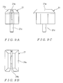
- a pair of guide pins 20 are provided on the first housing 10 in positions corresponding to the guide pin accommodating recessed parts 14. As is shown in Figs. 5A and 5B, and 8A through 8C, each of the guide pins 20 is provided so as to be movable upward and downward with respect to the corresponding guide pin accommodating recessed part 14 in the first housing 10, and is constructed from a cover housing 21 that protrudes upward from the mating surface of the mating part 12 (upper end surface of the mating part 12) and a spring member 22 that constantly drives the cover housing 21 upward. As is clearly shown in Figs.
- each cover housing 21 comprises a guide part 21 a whose tip end is tapered and a spring supporting part 21 c which protrudes downward from the guide part 21a, and is formed by molding an insulating resin.
- a locking plate accommodating groove 21b that extends in the forward-rearward direction and that opens on the front is formed in the guide part 21 a of the cover housing 21 of the guide pin 20 on the left side in the direction of length;
- a locking plate accommodating groove 21b that extends in the forward-rearward direction and that opens on the rear is formed in the guide part 21a of the cover housing 21 of the guide pin 20 on the right side in the direction of length.
- the spring members 22 are constructed from compression springs, and as is shown in Figs. 5B and 8A through 8C, the upper portions thereof are fitted over and supported by the spring supporting members 21c of the cover housings 22.
- the lower portions of the spring members 22 are accommodated inside the spring member accommodating recessed parts 15 in the first housing 10 as shown in Fig. 5B, and constantly drive the cover members 21 upward by means of the actions of the spring members 22.
- the locking plate 23 that is fastened to the cover housing 21 on the left side of the first housing 10 in the direction of length comprises a base plate part 23a that extends in the forward-rearward direction and that is accommodated in the corresponding locking plate accommodating groove 21b, and a press-fitting fastening part 23b that extends downward from the rear end of the base plate part 23a and that is press-fitted to the guide part 21a.
- a contact protruding part 23c is formed at the front end of the base plate part 23a via a flexible part that extends downward at an inclination toward the front, and a locking projection 23d that protrudes forward is formed below the contact protruding part 23c.
- the locking plate 23 is formed by stamping a metal plate.
- the locking plate 23 that is fastened to the cover housing 21 on the right side of the first housing 10 in the direction of length comprises a base plate part 23a that extends in the forward-rearward direction and that is accommodated in the corresponding locking plate accommodating groove 21b, and a press-fitting fastening part 23b that extends downward from the front end of the base plate part 23a and that is press-fitted to the guide part 21a.
- a contact protruding part 23c is formed at the rear end of the base plate part 23a via a flexible part that extends downward at an inclination toward the rear, and a locking projection 23d that protrudes rearward is formed below the contact protruding part 23c.
- metal fastening fittings 24 for fastening the first connector 1 to the circuit board PCB1 are attached to both ends of the mating part 12 of the first housing 10 in the direction of length. As is shown in Figs. 1 through 3, 5A and 5B, and 6A and 6B, metal fastening fittings 24 for fastening the first connector 1 to the circuit board PCB1 are attached to both ends of the mating part 12 of the first housing 10 in the direction of length. As is shown in Figs.
- These press-fitting fastening parts 24b are press-fitted to the corresponding board mounting part 13 of the first housing 10, and the board fastening parts 24f are fastened to the circuit board PCB1 by passing through the board mounting part 13.
- a locking piece 24c extends upward from the upper portion of the right end of the C-shaped bent part at the front end of the base plate part 24a.
- a locking hole 24d into which the locking projection 23d of the locking plate 23 is locked is formed in the upper portion of the locking piece 24c.
- a supporting part 24e for supporting the upper end of the locking piece 24c on the mating part 12 of the first housing 10 is provided on the upper end of the locking piece 24c. The supporting part 24e is provided in order to prevent the locking projection 23d from being easily disengaged from the locking hole 24d. The reason for this is that the positioning precision of the locking plate 23 inside the first housing 10 is required to cause the locking plate 23 to perform a locking action.
- the fastening fitting 24 is formed by stamping and forming a metal plate.
- the fastening fitting 24 that is attached to the right end of the mating part 12 in the direction of length comprises a C-shaped base plate part 24a that extends in the forward-rearward direction, a pair of press-fitting fastening parts 24b that extend downward from the two ends (front and rear ends) of the base plate part 24a, and a pair of board fastening parts 24f that extend downward from the portion of the base plate part 24a between the press-fitting fastening parts 24b.
- press-fitting fastening parts 24b are press-fitted to the corresponding board mounting part 13 of the first housing 10, and the board fastening parts 24f are fastened to the circuit board PCB1 by passing through the board mounting part 13.
- a locking piece 24c extends upward from the upper portion of the left end of the C-shaped bent part at the rear end of the base plate part 24a.
- a locking hole 24d into which the locking projection 23d of the locking plate 23 is locked is formed in the upper portion of the locking piece 24c.
- a supporting part 24e for supporting the upper end of the locking piece 24c on the mating part 12 of the first housing 10 is provided on the upper end of the locking piece 24c.
- the supporting part 24e is provided in order to prevent the locking projection 23d from being easily disengaged from the locking hole 24d.
- the reason for this is that the positioning precision of the locking plate 23 inside the first housing 10 is required to cause the locking plate 23 to perform a locking action.
- the fastening fitting 24 is formed by stamping and forming a metal plate.
- the system is constructed so that the vertical movement of the cover housings 21 is locked by the locking projections 23d of the locking plates 23 being locked into the locking holes 24d in the fastening fittings 24; thus, the locking plates 23 and fastening fittings 24 constitute the "locking means" referred to in Claims 1 and 2.
- the tine plate 30 comprises a base plate part 31 that extends in the direction of length, a pair of locking arms 32 that extend upward from either end of the base plate part 31 in the direction of length, and a plurality of positioning posts 33 that protrude downward from the vicinity of both ends of the base plate part 31 in the direction of length.
- a plurality of through-holes 31a through which these leg parts pass are formed in the base plate part 31.
- the tine plate 30 is designed to move between the initial position shown in Fig. 1 and the final position that is located above the initial position (although this final position is not shown in the figures).
- the second connector 41 that mates with the first connector 1 is designed to be mounted on a circuit board PCB2 that is provided on the other side, i.e., on the side of the personal computer (not shown in the figures). Furthermore, the second connector 41 comprises an insulating second housing 50, a plurality of contacts 54 that are attached to the second housing 50, and a tine plate 60 for aligning the leg parts of the contacts 54. The contacts 54 are connected by soldering to the circuit board PCB2.
- the second housing 50 extends in the direction of length (left-right direction in Fig. 11), and is formed by molding an insulating resin.
- a mating recessed part 51 that opens above and that extends in the direction of length is formed in the second housing 50, so that the mating part 12 of the first connector 1 is caused to mate into this mating recessed part 51.
- a front wall part 51a that extends in the direction of length and a rear wall part 51b that is provided on the rear with a specified space left from this front wall part 51a and that extends in the direction of length are provided in an upright attitude inside the mating recessed part 51.
- the contacts 54 are provided in four rows, i.e., both on the front and rear ends of the front wall part 51a and both on the front and rear ends of the rear wall part 51b, and are designed to make contact with the contacts 16 of the first connector 1 when the first connector 1 and the second connector 41 mate.
- a blind plate 52 that covers the mating recessed part 51 is provided in the mating recessed part 51 so that this blind plate 52 can move upward and downward as shown in Fig. 13D.
- the blind plate 52 is constantly driven upward by compression springs 59 that are installed inside the mating recessed part 51.
- a pair of guide holes 53 into which the housing covers 21 of the guide pins 20 are inserted are formed in either end of the second housing 50 in the direction of length.
- metal shells 55 for shielding the second connector 41 are attached to the front and rear surfaces of the second housing 50.
- a pair of temporary locking pieces 58 for temporary locking the tine plate 60 in the initial position are formed to protrude downward on either end of each shell 55 in the direction of length, and tongue pieces 57 that are grounded to the circuit board PCB2 are formed to protrude downward slightly on the inside of the temporary locking pieces 58.
- tongue pieces 57 that are grounded to the circuit board PCB2 are formed to protrude downward slightly on the inside of the temporary locking pieces 58.
- a lock releasing part 56 that releases the locking of the locking plate 23 with respect to the corresponding fastening fitting 24 is formed at the left end (in the direction of length) of the front-side shell 55 by bending this shell 55 from the upper end of the shell 55 toward the interior of the corresponding guide hole 53.
- a lock releasing part 56 that releases the locking of the locking plate 23 with the corresponding fastening fitting 24 is also formed at the right end (in the direction of length) of the rear-side shell 55 by bending this shell 55 from the upper end of the shell 55 toward the interior of the corresponding guide hole 53. As is shown in Fig.
- these lock releasing parts 56 contact the contact protruding parts 23c of the locking plates 23 at the initial stage of insertion of the cover housings 21 into the guide holes 15, and release the locking by contacting the locking projections 23d of the locking plates 23 and displacing the locking projections 23d in the direction of arrow A in the process of insertion of the cover housings 21 into the guide holes 53 as shown in Fig. 15B.
- the lock releasing parts 56 slide the outer surfaces of the fastening fittings 24 as shown in Fig. 15C.
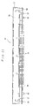
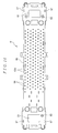
- the tine plate 60 is formed with a substantially rectangular shape that extends in the direction of length, and in order to align the leg parts of the respective contacts 54, a plurality of through-holes 60a through which these leg parts pass are formed.
- the tine plate 60 is designed to move between the initial position shown in Figs. 13A and 13D and the final position shown in Figs. 13B and 13C that is located above this initial position.
- the tine plate 60 is temporarily locked by the temporary locking pieces 58 in the initial position shown in Figs. 13A and 13D.
- a pair of openings 61 through which the cover housings 21 can pass are formed in either end portion of the tine plate 60 in the direction of length.
- a plurality of positioning posts 62 are formed to protrude downward on the undersurface of the tine plate 60 on both ends in the direction of length.
- the first connector 1 is mounted on the circuit board PCB1 that is provided on the side of the extension unit
- the second connector 41 is mounted on the circuit board PCB2 that is provided on the side of the personal computer. At this point, the tine plate 30 of the first connector 1 and the tine plate 60 of the second connector 41 are respectively located in the final position.
- the first connector 1 and the second connector 41 are caused to mate, with the first connector 1 on the side of the extension unit at the bottom and the second connector 41 on the side of the personal computer at the top while inserting the cover housings 21 of the first connector 1 into the guide holes 53 in the second connector 41. Then, the mating of the first connector 1 and the second connector 41 is guided by the cover housings 21 and the guide holes 53; since the vertical movement of the cover housings 21 is locked as a result of the locking projections 23d of the locking plates 23 being locked in the locking holes 24d in the fastening fittings 24, the mating of the first connector 1 and the second connector 41 is securely guided. Moreover, as is shown in Fig.
- the upper ends of the cover housings 21 pass through the openings 61 formed in the tine plate 60 of the second connector 41, and contact the circuit board PCB2.
- the cover housings 21 extend upward until this point, thus making it possible to ensure the sufficient amount of guiding.
- the lock releasing parts 56 slide the outer surfaces of the fastening fittings 24. Accordingly, the state of grounding of the first connector 1 and the second connector 41 is maintained.
- the cover housings 21 are compressed inside the guide holes 53 in the second connector 41 as a result of being pressed by the circuit board PCB2 as shown in Fig. 15C, so that portions of the cover housings 21 are positioned inside the guide pin accommodating recessed parts 14 in the first connector 1. Accordingly, the cover housings 21 do not protrude beyond the attachment surface of the second connector 41 with respect to the circuit board PCB2. Consequently, there is no need to form holes through which the guide pins (cover housings 21) are caused to pass in the circuit board PCB2 for mounting the second connector 41, thus making it possible to produce a docking connector that is suitable for high-density mounting.
- the locking means for locking the vertical movement of the cover housings 21 are constructed from the metal fastening fittings 24 that are provided on the first housing 10 and that are fastened to the circuit board PCB1 on one side, and the metal locking plates 23 that are provided on the cover housings 21 and that are locked with the fastening fittings 24.
- the lock releasing means for releasing the locking of the cover housings 21 by the locking means are constructed from the lock releasing parts 56 of the metal shells 55 that are provided on the second housing 50, that release the locking of the locking plates 23 with respect to the fastening fittings 24, and that are connected to the circuit board PCB2 on the other side. Accordingly, it is possible to constitute the locking means and lock releasing means with simple constructions.
- the fastening fittings 24 of the locking means have both the function of fastening the first housing 10 to the circuit board PCB1 and the function of locking the locking plates 23.
- the shells 55 have both the function of shielding the second connector 41 and the function of releasing the locking of the locking plates 23 with respect to the fastening fittings 24.
- the locking means from the metal fastening fittings that are provided on the first housing 10 and that are fastened to the circuit board PCB1 on one side, and the metal locking plates 23 that are provided on the cover housings 21 and that are locked with the fastening fittings 24.
- lock releasing means from the metal shells 55 that are provided on the second housing 50, that release the locking of the locking plates 23 with respect to the fastening fittings 24, and that are connected to the circuit board PCB2 on the other side.
Landscapes
- Details Of Connecting Devices For Male And Female Coupling (AREA)
- Coupling Device And Connection With Printed Circuit (AREA)
- Multi-Conductor Connections (AREA)
Applications Claiming Priority (1)
| Application Number | Priority Date | Filing Date | Title |
|---|---|---|---|
| JP2004226937A JP2006049036A (ja) | 2004-08-03 | 2004-08-03 | ドッキングコネクタ |
Publications (2)
| Publication Number | Publication Date |
|---|---|
| EP1624535A1 true EP1624535A1 (fr) | 2006-02-08 |
| EP1624535B1 EP1624535B1 (fr) | 2007-10-17 |
Family
ID=35044690
Family Applications (1)
| Application Number | Title | Priority Date | Filing Date |
|---|---|---|---|
| EP05107169A Expired - Fee Related EP1624535B1 (fr) | 2004-08-03 | 2005-08-03 | Connecteur d'accueil |
Country Status (7)
| Country | Link |
|---|---|
| US (1) | US7244138B2 (fr) |
| EP (1) | EP1624535B1 (fr) |
| JP (1) | JP2006049036A (fr) |
| KR (1) | KR20060049054A (fr) |
| CN (1) | CN1734853A (fr) |
| DE (1) | DE602005002885T2 (fr) |
| TW (1) | TWM288984U (fr) |
Cited By (2)
| Publication number | Priority date | Publication date | Assignee | Title |
|---|---|---|---|---|
| EP1701412A1 (fr) * | 2005-03-11 | 2006-09-13 | Huawei Technologies Co., Ltd. | Interface de connexion |
| US9743544B2 (en) | 2012-06-20 | 2017-08-22 | Lear Corporation | Positioning element |
Families Citing this family (14)
| Publication number | Priority date | Publication date | Assignee | Title |
|---|---|---|---|---|
| JP4971957B2 (ja) * | 2007-11-29 | 2012-07-11 | タイコエレクトロニクスジャパン合同会社 | コンタクト部材、コンタクト部材の保持構造及び電気コネクタ |
| CN101459297B (zh) * | 2007-12-14 | 2013-01-02 | 泰科电子(上海)有限公司 | 电气连接装置 |
| US20100195302A1 (en) * | 2009-02-03 | 2010-08-05 | Rigby William J | Flexible guiding module |
| KR100967354B1 (ko) * | 2009-03-19 | 2010-07-05 | 이성호 | 복합 입력 방식의 터치패널 |
| DE102009058616B4 (de) | 2009-12-17 | 2011-11-10 | Harting Electronics Gmbh & Co. Kg | Leiterplattensteckverbinder mit Verriegelungsvorrichtung |
| US8944697B2 (en) | 2012-09-28 | 2015-02-03 | Positronic Industries, Inc. | Fiber optic connector assembly |
| US9361601B2 (en) * | 2012-10-02 | 2016-06-07 | Kiosk Information Systems, Inc. | Systems and methods for locking and docking |
| CN103105911A (zh) * | 2013-01-30 | 2013-05-15 | 华一精密机械(昆山)有限公司 | 计算机用导电弹片装置 |
| WO2014121216A1 (fr) * | 2013-02-04 | 2014-08-07 | Siemens Healthcare Diagnostics Inc. | Appareil, systèmes et procédés d'accueil d'instruments |
| JP6317557B2 (ja) * | 2013-09-27 | 2018-04-25 | 株式会社エンプラス | 取付部材および電気部品用ソケット |
| CN109546417B (zh) * | 2017-09-21 | 2020-03-31 | 正凌精密工业(广东)有限公司 | 可顺利解锁的连接器壳体装置 |
| CN108134223B (zh) * | 2017-12-21 | 2019-06-18 | 郑州云海信息技术有限公司 | 一种pcba制备用直插式元件组合装置 |
| FR3108203B1 (fr) * | 2020-03-11 | 2023-06-02 | Axon Cable Sa | Ensemble de connexion à fixation rapide et sécurisée |
| US11158966B2 (en) * | 2020-03-26 | 2021-10-26 | TE Connectivity Services Gmbh | Collapsable alignment member |
Citations (7)
| Publication number | Priority date | Publication date | Assignee | Title |
|---|---|---|---|---|
| US5478253A (en) * | 1994-09-21 | 1995-12-26 | The Whitaker Corporation | Electrostatic discharge contacts for blind mating connectors |
| JPH08315910A (ja) | 1994-09-19 | 1996-11-29 | Molex Inc | ブラインド接続電気コネクタ |
| US5961337A (en) * | 1996-11-27 | 1999-10-05 | Norand Corporation | Universal charging and data communication apparatus |
| JPH11288760A (ja) | 1998-03-31 | 1999-10-19 | Jst Mfg Co Ltd | ドッキングコネクタ |
| JP2000089850A (ja) | 1998-09-09 | 2000-03-31 | Matsushita Electric Ind Co Ltd | ガイド機構を有する電子機器及び拡張ユニット |
| US20010031570A1 (en) * | 2000-04-17 | 2001-10-18 | International Business Machines Corporation | Flap actuation mechanism for an electronic unit |
| US6358067B1 (en) * | 1998-01-16 | 2002-03-19 | Molex Incorporated | Docking-style intermediate connector |
Family Cites Families (5)
| Publication number | Priority date | Publication date | Assignee | Title |
|---|---|---|---|---|
| JP3057546B2 (ja) * | 1995-02-23 | 2000-06-26 | モレックス インコーポレーテッド | ガイド機構付きコネクタ組立 |
| JP3148855B2 (ja) * | 1996-03-01 | 2001-03-26 | モレックス インコーポレーテッド | 電気コネクタ |
| US6074235A (en) * | 1998-04-07 | 2000-06-13 | The Whitaker Corporation | Alignment post having an improved locking feature |
| TW389402U (en) * | 1998-11-17 | 2000-05-01 | Hon Hai Prec Ind Co Ltd | Guiding device for connector |
| TWM266609U (en) * | 2004-07-16 | 2005-06-01 | Hon Hai Prec Ind Co Ltd | Electrical connector assembly |
-
2004
- 2004-08-03 JP JP2004226937A patent/JP2006049036A/ja active Pending
-
2005
- 2005-07-14 TW TW094211953U patent/TWM288984U/zh not_active IP Right Cessation
- 2005-08-02 CN CNA200510091906XA patent/CN1734853A/zh active Pending
- 2005-08-03 EP EP05107169A patent/EP1624535B1/fr not_active Expired - Fee Related
- 2005-08-03 KR KR1020050070879A patent/KR20060049054A/ko not_active Withdrawn
- 2005-08-03 DE DE602005002885T patent/DE602005002885T2/de not_active Expired - Lifetime
- 2005-08-03 US US11/196,648 patent/US7244138B2/en not_active Expired - Fee Related
Patent Citations (7)
| Publication number | Priority date | Publication date | Assignee | Title |
|---|---|---|---|---|
| JPH08315910A (ja) | 1994-09-19 | 1996-11-29 | Molex Inc | ブラインド接続電気コネクタ |
| US5478253A (en) * | 1994-09-21 | 1995-12-26 | The Whitaker Corporation | Electrostatic discharge contacts for blind mating connectors |
| US5961337A (en) * | 1996-11-27 | 1999-10-05 | Norand Corporation | Universal charging and data communication apparatus |
| US6358067B1 (en) * | 1998-01-16 | 2002-03-19 | Molex Incorporated | Docking-style intermediate connector |
| JPH11288760A (ja) | 1998-03-31 | 1999-10-19 | Jst Mfg Co Ltd | ドッキングコネクタ |
| JP2000089850A (ja) | 1998-09-09 | 2000-03-31 | Matsushita Electric Ind Co Ltd | ガイド機構を有する電子機器及び拡張ユニット |
| US20010031570A1 (en) * | 2000-04-17 | 2001-10-18 | International Business Machines Corporation | Flap actuation mechanism for an electronic unit |
Non-Patent Citations (1)
| Title |
|---|
| PATENT ABSTRACTS OF JAPAN vol. 2000, no. 01 31 January 2000 (2000-01-31) * |
Cited By (3)
| Publication number | Priority date | Publication date | Assignee | Title |
|---|---|---|---|---|
| EP1701412A1 (fr) * | 2005-03-11 | 2006-09-13 | Huawei Technologies Co., Ltd. | Interface de connexion |
| US7713085B2 (en) | 2005-03-11 | 2010-05-11 | Huawei Technologies Co., Ltd. | Connector interface |
| US9743544B2 (en) | 2012-06-20 | 2017-08-22 | Lear Corporation | Positioning element |
Also Published As
| Publication number | Publication date |
|---|---|
| DE602005002885D1 (de) | 2007-11-29 |
| JP2006049036A (ja) | 2006-02-16 |
| US20060030196A1 (en) | 2006-02-09 |
| KR20060049054A (ko) | 2006-05-18 |
| DE602005002885T2 (de) | 2008-05-21 |
| EP1624535B1 (fr) | 2007-10-17 |
| US7244138B2 (en) | 2007-07-17 |
| CN1734853A (zh) | 2006-02-15 |
| TWM288984U (en) | 2006-03-21 |
Similar Documents
| Publication | Publication Date | Title |
|---|---|---|
| EP1624535B1 (fr) | Connecteur d'accueil | |
| US7273382B2 (en) | Electrical connector and electrical connector assembly | |
| KR100480196B1 (ko) | 전선 접속기구 | |
| US7134895B1 (en) | PC board assembly | |
| US20220181811A1 (en) | Card edge connector with a locking system | |
| US7186126B2 (en) | Floating electrical connector | |
| US10243305B1 (en) | Electrical connector assembly | |
| CN114784552B (zh) | 电连接器以及连接器组件 | |
| USRE38089E1 (en) | Card connector | |
| JP2002139652A (ja) | 可動接続部を有する光コネクタと印刷回路基板の装置 | |
| CN210015997U (zh) | 板对板连接器组件 | |
| JPH1032060A (ja) | モジュール形コネクタ | |
| US20090111296A1 (en) | Latching device used for locking two daughter printed circuit boards in connector set | |
| EP0974176B1 (fr) | Connecteur guide flottant et son procede d'utilisation | |
| US7056136B2 (en) | Floating connector and method for manufacturing therefor | |
| CN117220081A (zh) | 连接器组件 | |
| JP3282802B2 (ja) | 中継コネクタ組立体及びそれに使用されるケーブル側コネクタ | |
| US12519257B2 (en) | Electrical connector to achieve required coplanarity of terminal parts of receptacle, method for manufacturing electrical connector, and method for mounting electrical connector | |
| JP3748787B2 (ja) | 可動型コネクタ | |
| US20240006789A1 (en) | Electrical connector and method for manufacturing electrical connector | |
| JP3467427B2 (ja) | コネクタの装着構造 | |
| KR200438442Y1 (ko) | 래치를 구비한 커넥터 안내부와 커넥터 | |
| CN120109565A (zh) | 一种高速电连接器及其制造方法 | |
| US7165985B2 (en) | Connector apparatus provided with a lever having a rotating end used in coupling of the connector apparatus | |
| WO2003055006A1 (fr) | Structure de broche de renfort de connecteur electrique |
Legal Events
| Date | Code | Title | Description |
|---|---|---|---|
| PUAI | Public reference made under article 153(3) epc to a published international application that has entered the european phase |
Free format text: ORIGINAL CODE: 0009012 |
|
| AK | Designated contracting states |
Kind code of ref document: A1 Designated state(s): AT BE BG CH CY CZ DE DK EE ES FI FR GB GR HU IE IS IT LI LT LU LV MC NL PL PT RO SE SI SK TR |
|
| AX | Request for extension of the european patent |
Extension state: AL BA HR MK YU |
|
| GRAP | Despatch of communication of intention to grant a patent |
Free format text: ORIGINAL CODE: EPIDOSNIGR1 |
|
| 17P | Request for examination filed |
Effective date: 20060803 |
|
| AKX | Designation fees paid |
Designated state(s): DE FR GB |
|
| GRAS | Grant fee paid |
Free format text: ORIGINAL CODE: EPIDOSNIGR3 |
|
| GRAA | (expected) grant |
Free format text: ORIGINAL CODE: 0009210 |
|
| AK | Designated contracting states |
Kind code of ref document: B1 Designated state(s): DE FR GB |
|
| REG | Reference to a national code |
Ref country code: GB Ref legal event code: FG4D |
|
| REF | Corresponds to: |
Ref document number: 602005002885 Country of ref document: DE Date of ref document: 20071129 Kind code of ref document: P |
|
| ET | Fr: translation filed | ||
| PLBE | No opposition filed within time limit |
Free format text: ORIGINAL CODE: 0009261 |
|
| STAA | Information on the status of an ep patent application or granted ep patent |
Free format text: STATUS: NO OPPOSITION FILED WITHIN TIME LIMIT |
|
| 26N | No opposition filed |
Effective date: 20080718 |
|
| PGFP | Annual fee paid to national office [announced via postgrant information from national office to epo] |
Ref country code: FR Payment date: 20090817 Year of fee payment: 5 |
|
| PGFP | Annual fee paid to national office [announced via postgrant information from national office to epo] |
Ref country code: GB Payment date: 20090825 Year of fee payment: 5 |
|
| PGFP | Annual fee paid to national office [announced via postgrant information from national office to epo] |
Ref country code: DE Payment date: 20090827 Year of fee payment: 5 |
|
| REG | Reference to a national code |
Ref country code: FR Ref legal event code: CD |
|
| GBPC | Gb: european patent ceased through non-payment of renewal fee |
Effective date: 20100803 |
|
| REG | Reference to a national code |
Ref country code: FR Ref legal event code: ST Effective date: 20110502 |
|
| REG | Reference to a national code |
Ref country code: DE Ref legal event code: R119 Ref document number: 602005002885 Country of ref document: DE Effective date: 20110301 |
|
| PG25 | Lapsed in a contracting state [announced via postgrant information from national office to epo] |
Ref country code: DE Free format text: LAPSE BECAUSE OF NON-PAYMENT OF DUE FEES Effective date: 20110301 Ref country code: FR Free format text: LAPSE BECAUSE OF NON-PAYMENT OF DUE FEES Effective date: 20100831 |
|
| PG25 | Lapsed in a contracting state [announced via postgrant information from national office to epo] |
Ref country code: GB Free format text: LAPSE BECAUSE OF NON-PAYMENT OF DUE FEES Effective date: 20100803 |