EP1625663B1 - Circuit integre et procede de programmation d'un circuit integre - Google Patents
Circuit integre et procede de programmation d'un circuit integre Download PDFInfo
- Publication number
- EP1625663B1 EP1625663B1 EP04727877.5A EP04727877A EP1625663B1 EP 1625663 B1 EP1625663 B1 EP 1625663B1 EP 04727877 A EP04727877 A EP 04727877A EP 1625663 B1 EP1625663 B1 EP 1625663B1
- Authority
- EP
- European Patent Office
- Prior art keywords
- circuit arrangement
- component
- integrated circuit
- comparator
- external
- Prior art date
- Legal status (The legal status is an assumption and is not a legal conclusion. Google has not performed a legal analysis and makes no representation as to the accuracy of the status listed.)
- Expired - Lifetime
Links
- 238000000034 method Methods 0.000 title claims description 13
- 239000003990 capacitor Substances 0.000 claims description 20
- 230000006870 function Effects 0.000 claims description 14
- 230000003213 activating effect Effects 0.000 claims description 3
- 230000003139 buffering effect Effects 0.000 claims 1
- 230000004913 activation Effects 0.000 description 5
- 238000004519 manufacturing process Methods 0.000 description 5
- 238000001465 metallisation Methods 0.000 description 3
- 230000008901 benefit Effects 0.000 description 1
- 238000005266 casting Methods 0.000 description 1
- 238000006243 chemical reaction Methods 0.000 description 1
- 238000010276 construction Methods 0.000 description 1
- 230000001419 dependent effect Effects 0.000 description 1
- 238000012986 modification Methods 0.000 description 1
- 230000004048 modification Effects 0.000 description 1
- 229910021420 polycrystalline silicon Inorganic materials 0.000 description 1
- 229920005591 polysilicon Polymers 0.000 description 1
- 230000008569 process Effects 0.000 description 1
- 230000009467 reduction Effects 0.000 description 1
- 230000004044 response Effects 0.000 description 1
Images

Classifications
-
- H—ELECTRICITY
- H03—ELECTRONIC CIRCUITRY
- H03K—PULSE TECHNIQUE
- H03K19/00—Logic circuits, i.e. having at least two inputs acting on one output; Inverting circuits
- H03K19/02—Logic circuits, i.e. having at least two inputs acting on one output; Inverting circuits using specified components
- H03K19/173—Logic circuits, i.e. having at least two inputs acting on one output; Inverting circuits using specified components using elementary logic circuits as components
-
- H—ELECTRICITY
- H03—ELECTRONIC CIRCUITRY
- H03K—PULSE TECHNIQUE
- H03K19/00—Logic circuits, i.e. having at least two inputs acting on one output; Inverting circuits
- H03K19/02—Logic circuits, i.e. having at least two inputs acting on one output; Inverting circuits using specified components
- H03K19/173—Logic circuits, i.e. having at least two inputs acting on one output; Inverting circuits using specified components using elementary logic circuits as components
- H03K19/1731—Optimisation thereof
- H03K19/1732—Optimisation thereof by limitation or reduction of the pin/gate ratio
Definitions
- the present invention relates to an integrated circuit device and a method for programming an integrated circuit device.
- the described programming of an integrated component could, for example, subsequently be determined by fuse banks, DIP switches or the like.
- the document US 6,351,175 B1 relates to a mode selection circuit.
- a mode select terminal is selectively connected to a configuration element to bias the mode select terminal to one of a plurality of predetermined voltages.
- a voltage divider provides several voltages.
- the object of the present invention is to provide an integrated circuit arrangement which, after the end of production, can be programmed with little effort, ie can be put into a desired operating mode.
- a further object of the invention is to specify a method for programming an integrated circuit arrangement which can be carried out with little effort and enables the operation of the integrated circuit arrangement in an operating mode which can be selected after the end of production.
- the programming for example the selection of one of several predetermined operating modes, of the integrated circuit arrangement takes place in that an external, readable component is connected to the connection of the integrated circuit arrangement.
- This component has a readable value, for example a specific resistance value, which is compared with a reference value of a reference component.
- the integrated circuit arrangement is set by the control unit in a specific mode, that is programmed.
- the external, readable component is preferably a passive component.
- a signal source is provided, for example, in the integrated circuit arrangement, which generates a reference signal with which the external, readable component is applied.
- the further connection of the external, readable component is preferably connectable to a reference potential terminal, for example ground.
- the comparator which compares the value of the external readable component with the value of the reference component, preferably comprises an analogue to digital converter for outputting the comparison result in digital form.
- an A / D converter with a resolution of 3 bits can be provided, so that a total of 8 different operating states can be activated by simply selecting the value of the readable component to be connected.
- the analog / digital converter has according to a preferred development of the circuit arrangement a logarithmic characteristic.
- a logarithmic characteristic As a result, the requirements for the tolerance of the external, readable component and the tolerances in the Further processing of the read value significantly reduced.
- an external readable component with a tolerance of 30% due to the logarithmic characteristic can still be reliably read and reliably select one of several predetermined modes.
- the reference component can be provided as an externally connectable component or as a component integrated on the circuit arrangement.
- an external reference component which is connected to a terminal pin (pin) of the integrated circuit arrangement, is anyway often provided to generate high-precision reference signals, for example bias currents.
- This may be, for example, an external filter capacitor.
- This component is also used as a reference component for the programming of the integrated circuit arrangement according to the proposed principle. For determining the comparison result, the external reference component is also acted upon by the reference signal output by the signal source, and the value of the reference component is read out.
- An external reference component has lower tolerances than an integrated reference component.
- the embodiment of the reference component as an integrated component is advantageous in particular if an external reference component is not required anyway for the functionality of the integrated circuit and / or a particularly small number of pins of the circuit arrangement is required.
- the reference component and the readable, programming component are designed as a capacitor.
- the integrated circuit arrangement can comprise a plurality of functional blocks, wherein the control unit can control these function blocks with different supply voltage, reference voltage and / or switch-on sequence depending on the comparison result of the comparator.
- a so-called latch for latching the comparison result of the comparator.
- the readout of the readable value of the external, readable component and the comparison of this value with the value of the reference component preferably takes place during a switch-on phase of the integrated circuit arrangement.
- a memory block is preferably provided for storing control parameters for the respective operating modes. This memory block is coupled to the control unit in such a way that one of the stored operating modes is activated as a function of the comparison result of the comparator.
- the memory block is preferably designed as a so-called boot ROM (Read Only Memory) and is read when switching on the integrated circuit arrangement.
- boot ROM Read Only Memory
- the boot ROM may be programmable, for example, by selecting masks for the metallization levels of the programmable boot ROM during manufacture.
- the described principle is preferably applicable to so-called power management units, PMU, in order to control the power-on sequence.
- PMU power management units
- the various predeterminable sequences may be stored and defined in the ROM and are selected in the application by the value of the programmable, readable component.
- a still further increase in flexibility is obtained by providing a programmable ROM with so-called zener or poly-fuses, ie programmable connections, instead of the metal-mask programmable ROM.
- a programmable ROM with so-called zener or poly-fuses, ie programmable connections, instead of the metal-mask programmable ROM.
- the conductivity state of the fuse is determined by applying an energy pulse, wherein the conductivity state can be switched between high-impedance and low-impedance.
- the reference component is provided as an integrated component, then it may be advantageous to increase the accuracy by a simple adjustment possibility of the integrated reference component.
- an activation circuit which is coupled to respective activation inputs of the comparator and / or signal source.
- the activation circuit is designed to activate the comparator and, if appropriate, the signal source after switching on the integrated circuit and switches them off again as soon as the comparison, if appropriate with analog / digital conversion, is ended and the comparison result is stored.
- the object is achieved by a method for programming an integrated circuit arrangement, comprising the method steps of claim 11.
- an external, readable component is connected to the integrated circuit arrangement and then the value of this external readable component is read out. This value is then compared with the likewise read value of a reference component, ie a reference value, and a comparison result is determined. In response to this comparison result, a selection signal is output for controlling the integrated circuit.
- the integrated circuit arrangement is offset in one of a plurality of predetermined operating states as a function of the selection signal.
- the reference value is determined by reading an external or integrated reference component.
- the comparison of reference value and the value of the external readable component is preferably carried out with the aid of an analog / digital converter.
- the values of the readable external component and the reference component are read out by applying the same to a reference signal provided by a signal source, preferably during a switch-on operation of the integrated circuit arrangement.
- the comparison result is cached after its determination in a volatile memory so that it is ready even after the end of the power-on.
- the comparison is activated during a switch-on process, and then the comparator, which carries out the comparison and, if appropriate, the signal source which is used to read out the readable component values, are deactivated again.
- the reference signal provided by the signal source may be, for example, a reference voltage or a reference current.
- an external filter capacitor or a similar external passive component is provided anyway, this can preferably be used as a reference component.
- two pins are provided, to which the external readable component and the reference component can be connected in each case.
- the respective free end of such passive components is preferably connected to a reference potential terminal, such as ground.
- the described method makes it possible with little effort that, depending on the value of a passive component which can be connected to a pin of the integrated circuit arrangement, the integrated circuit arrangement can be put into one of a plurality of predetermined operating modes.
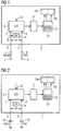
- FIG. 1 shows an integrated circuit arrangement 1, which among other things has two terminals 2, 3, so-called pins.
- To the terminal 2 of the integrated circuit arrangement 1 is an external, readable component in the form of a resistor 4 against a reference potential terminal 5 is turned on.
- the resistor 4 is used, as explained in more detail later, for programming the circuit arrangement 1.
- the terminals 2, 3 of the circuit arrangement 1 are connected internally to a first or a second input 7, 8 of a comparator 9.
- the comparator 9 comprises an analog / digital converter.
- the comparator 9 has an enable input 10 for activating the comparator 9 during a switch-on phase.
- To the digital output of the A / D converter using the Output of the comparator 9 is connected via a volatile memory 11, a control unit 12 which controls a plurality of functional blocks 13 a, 13 b in the circuit arrangement 1.
- a signal source 14 is provided, which is designed to generate a reference signal and which is connected to the terminals 2, 3 of the circuit arrangement.
- the reference component 6 serves not only as a reference component for the comparator 9 according to the proposed principle, but also as a reference resistor for generating a bias signal, which is required for the function of at least one of the function blocks 13a, 13b anyway.
- the readable, programmable resistor 4 and the reference resistor 6 are supplied with a reference signal which generates the reference source 14, ie with a reference voltage or a reference current.
- the comparator 9 compares the signals which occur at its inputs 7, 8, which of course depend on the component values Rprog, Rref of the resistors 4, 6, with each other.
- the A / D converter determines the ratio of the values Rprog, Rref of the two external components 4, 6, and outputs a corresponding comparison result at the output in digital form. This comparison result is buffered in the latch 11. Subsequently, the comparator 9 with the A / D converter and the signal source 14 are deactivated.
- control unit 12 With the comparison result stored in the memory 11, it is now possible for the control unit 12 to control the function blocks 13a, 13b of the circuit arrangement. This is done according to the proposed principle as a function of the value of the programming resistor 4.
- the additional resistor 4 may be a simple and inexpensive external resistor to which low tolerance requirements are to be placed.
- a further reduction in the requirements for the tolerance accuracy of the resistor 4 is achieved in that the A / D converter in the comparator 9 has a logarithmic characteristic.
- boot ROM for each adjustable operating mode, a plurality of parameters, such as e.g. Supply voltage levels for certain functional blocks 13a, 13b, reference voltage level, Einschalt Holn Kunststoff etc. stored in boot ROM.
- the boot ROM is mask-programmable by varying the metallization. This ROM is addressed by the result of the comparator 9.
- the available power up sequences, one of which can be selected with the resistor 4 are thus defined by metallization masks and selected in the application by the value of the programming device 4.
- ROM is implemented in the control unit 12 as a programmable ROM and this zener or polysilicon fuses has.
- the described principle is applicable for controlling the power-up sequence in power supply units, English Power Management Units, PMU.
- FIG. 2 shows an alternative embodiment of the integrated circuit of FIG. 1 ,
- the circuit of Figure 2 corresponds in structure and in its advantageous operation largely that of FIG. 1 and should not be described again at this point.
- a programming capacitor 15 and a reference capacitance 16 are provided. These are also connected between external terminals 2, 3 of the chip 1 and reference potential 5.
- the reference capacitor 16 is on the chip 1 of FIG. 2 anyway for the operation of at least one functional block 13a, 13b provided as a filter capacitor.
- the capacitors 15, 16 are charged by the signal source 14 upon activation of the comparator 9 and the signal source 14 at the input 10 and the self-adjusting signals applied to inputs 7, 8 of the comparator 9 and the capacitance values Cprog, Cref of the capacitors 15, 16 are evaluated by this.
- the remaining functionality corresponds to that in FIG. 1 already explained.
- FIG. 3 shows an alternative embodiment FIG. 1 , which largely coincides with this in construction and advantageous operation. In that regard, the description of the figures will not be repeated here.
- an integrated reference resistor 17 which is connected between the input 8 of the comparator 9 and an internal reference potential terminal 5 '. This eliminates the external pin 3 on the chip. 1
- the described embodiment has the advantage that fewer connection pins are required on the chip and is then preferably used, for example, if an external reference component is not required anyway, for example for generating a precise reference signal or as a filter component.
- FIG. 4 shows an alternative embodiment of the circuit of FIG. 2 , Instead of the external reference capacitor 16 of FIG. 2 is at the circuit of FIG. 4 an integrated capacitor 18 is provided. The capacitor 18 is connected between the input 8 of the comparator 9 and reference potential 5 '.
- FIG. 3 eliminates a pin, namely the terminal 3.
- the embodiment shown is advantageously used, if not anyway an external filter capacitor is required as a reference component.
- reference components 17, 18 of FIGS. 3, 4 may be advantageous to provide an adjustment possibility for the adjustment of the respective internal, passive reference component 17, 18th
- resistors and capacitors shown in the exemplary embodiments as a reference component and as a programmable, readable component, it is also possible to provide other, passive components.
Landscapes
- Physics & Mathematics (AREA)
- Engineering & Computer Science (AREA)
- Computer Hardware Design (AREA)
- Computing Systems (AREA)
- General Engineering & Computer Science (AREA)
- Mathematical Physics (AREA)
- Semiconductor Integrated Circuits (AREA)
- Design And Manufacture Of Integrated Circuits (AREA)
- Logic Circuits (AREA)
Claims (13)
- Agencement de circuit (1) intégré, présentant- un comparateur (9) doté d'une première entrée (7) qui est reliée à une connexion (2) de l'agencement de circuit intégré, conçu pour la connexion d'un composant (15) externe lisible constitué comme condensateur avec une valeur (Cprog) issue d'une quantité de valeurs prédéterminée, doté d'une deuxième entrée (8) à laquelle un composant de référence (16, 18) lisible est connecté, lequel est un condensateur de référence externe de toute façon prévu comme condensateur de filtrage pour le fonctionnement d'au moins un bloc fonctionnel, ou une capacité intégrée, et doté d'une sortie,- l'agencement de circuit (1) présentant en outre une unité de commande (12) qui est couplée à la sortie du comparateur (9) pour la commande de l'agencement de circuit (1) intégré en fonction d'un résultat de comparaison du comparateur (9), sachant que- une source de signal (14) destinée à générer un signal de référence est prévue, laquelle est couplée à la connexion (2) destinée à connecter un composant (15) externe lisible et au composant de référence (16, 18) pour la lecture de la valeur de composant respective (Cprog, Cref).
- Agencement de circuit selon la revendication 1,
caractérisé en ce que
le composant (15) externe lisible est couplé à une connexion de potentiel de référence (5) via une connexion supplémentaire. - Agencement de circuit selon l'une des revendications 1 à 2,
caractérisé en ce que
le comparateur (9) comprend un convertisseur analogique-numérique destiné à délivrer le résultat de comparaison sous forme numérique. - Agencement de circuit selon la revendication 3,
caractérisé en ce que
le convertisseur analogique-numérique a une courbe caractéristique logarithmique. - Agencement de circuit selon l'une des revendications 1 à 4,
caractérisé en ce que
le composant de référence est apte à être connecté comme composant (16) externe au niveau d'une connexion (3) supplémentaire de l'agencement de circuit (1) intégré. - Agencement de circuit selon l'une des revendications 1 à 4,
caractérisé en ce que
le composant de référence est prévu comme composant intégré (18) de l'agencement de circuit (1) intégré. - Agencement de circuit selon l'une des revendications 1 à 6,
caractérisé en ce que
plusieurs blocs fonctionnels (13a, 13b) sont prévus, lesquels sont pilotés par l'unité de commande (12) en matière de tension d'alimentation, de tension de référence et/ou de séquence de mise en marche. - Agencement de circuit selon l'une des revendications 1 à 7,
caractérisé en ce que
une mémoire volatile (11) est montée entre la sortie du comparateur (9) et l'unité de commande (12) pour la mise en mémoire tampon du résultat de comparaison du comparateur (9). - Agencement de circuit selon l'une des revendications 1 à 8,
caractérisé en ce que
un bloc mémoire (19) destiné à classer des paramètres de commande selon plusieurs modes de fonctionnement de l'au moins un bloc fonctionnel (13a, 13b) de l'agencement de circuit (1) est prévu, lequel est couplé à l'unité de commande (12) ou inclus par celle-ci, sachant qu'en fonction du résultat de comparaison du comparateur (9), l'un des modes de fonctionnement mémorisés est activé. - Agencement de circuit selon l'une des revendications 1 à 9,
caractérisé en ce que
le comparateur (9) présente une entrée d'activation (10) destinée à activer le comparateur (9) après la mise en marche du circuit (1) intégré. - Procédé de programmation d'un agencement de circuit intégré, comprenant les étapes de procédé suivantes:- lecture d'une valeur (Cprog) d'un composant (15) externe constitué comme condensateur et connecté à l'agencement de circuit intégré,- comparaison de la valeur (Cprog) lue avec une valeur de référence (Cref) d'un composant de référence, lequel est un condensateur de référence externe de toute façon prévu comme condensateur de filtrage pour le fonctionnement d'au moins un bloc fonctionnel, ou une capacité intégrée, et détermination d'un résultat de comparaison,- délivrance d'un signal de sélection pour la commande de l'agencement de circuit (1) intégré en fonction du résultat de comparaison,- dans lequel la valeur (Cprog) du composant (15) externe connecté à l'agencement de circuit intégré est lue par application d'un signal de référence au composant et- dans lequel la valeur de référence (Cref) est représentée par la valeur d'un composant de référence (16, 18) qui est également lue par application du signal de référence.
- Procédé selon la revendication 11,
dans lequel l'agencement de circuit (1) est mis dans un état de fonctionnement prédéterminé issu d'une quantité d'états de fonctionnement prédéterminés en fonction du signal de sélection. - Procédé selon l'une des revendications 11 à 12,
dans lequel le résultat de comparaison est déterminé pendant une opération de mise en marche de l'agencement de circuit intégré et mis en mémoire tampon dans une mémoire volatile (11).
Applications Claiming Priority (2)
| Application Number | Priority Date | Filing Date | Title |
|---|---|---|---|
| DE10323012A DE10323012B4 (de) | 2003-05-21 | 2003-05-21 | Programmierbare, integrierte Schaltungsanordnung und Verfahren zur Programmierung einer integrierten Schaltungsanordnung |
| PCT/EP2004/004079 WO2004105246A2 (fr) | 2003-05-21 | 2004-04-16 | Circuit integre et procede de programmation d'un circuit integre |
Publications (2)
| Publication Number | Publication Date |
|---|---|
| EP1625663A2 EP1625663A2 (fr) | 2006-02-15 |
| EP1625663B1 true EP1625663B1 (fr) | 2017-03-22 |
Family
ID=33441102
Family Applications (1)
| Application Number | Title | Priority Date | Filing Date |
|---|---|---|---|
| EP04727877.5A Expired - Lifetime EP1625663B1 (fr) | 2003-05-21 | 2004-04-16 | Circuit integre et procede de programmation d'un circuit integre |
Country Status (7)
| Country | Link |
|---|---|
| US (1) | US7724167B2 (fr) |
| EP (1) | EP1625663B1 (fr) |
| JP (1) | JP4286283B2 (fr) |
| KR (1) | KR100734590B1 (fr) |
| CN (1) | CN100361391C (fr) |
| DE (1) | DE10323012B4 (fr) |
| WO (1) | WO2004105246A2 (fr) |
Families Citing this family (6)
| Publication number | Priority date | Publication date | Assignee | Title |
|---|---|---|---|---|
| DE102005055886B4 (de) * | 2005-11-23 | 2015-03-26 | Austriamicrosystems Ag | Halbleiterkörper, Schaltungsanordnung mit dem Halbleiterkörper und Verfahren |
| US9077365B2 (en) | 2010-10-15 | 2015-07-07 | S.C. Johnson & Son, Inc. | Application specific integrated circuit including a motion detection system |
| JP2015106900A (ja) * | 2013-12-03 | 2015-06-08 | ダイヤモンド電機株式会社 | Ad変換処理装置 |
| US9843338B1 (en) | 2017-03-20 | 2017-12-12 | Silanna Asia Pte Ltd | Resistor-based configuration system |
| CN113704170B (zh) * | 2021-07-30 | 2024-02-09 | 浪潮电子信息产业股份有限公司 | 一种芯片工作模式控制方法、系统及介质 |
| US20250077243A1 (en) * | 2023-09-05 | 2025-03-06 | Xilinx, Inc. | Randomization of instruction execution flow for glitch protection |
Family Cites Families (23)
| Publication number | Priority date | Publication date | Assignee | Title |
|---|---|---|---|---|
| JP2623000B2 (ja) | 1989-01-19 | 1997-06-25 | 三洋電機株式会社 | マイクロコンピュータのリセット機構 |
| JP2839288B2 (ja) | 1989-07-15 | 1998-12-16 | 旭化成工業株式会社 | ビスコースレーヨンフィラメント糸 |
| US5157397A (en) * | 1991-01-28 | 1992-10-20 | Trw Inc. | Quantizer and related method for improving linearity |
| KR950002162B1 (ko) * | 1992-02-12 | 1995-03-14 | 삼성전자주식회사 | Cpu 로직의 자동 절환 장치 |
| JPH08147076A (ja) * | 1994-11-22 | 1996-06-07 | Seiko Epson Corp | 情報処理装置 |
| DE69514783T2 (de) * | 1995-03-23 | 2000-06-08 | Stmicroelectronics S.R.L., Agrate Brianza | Leseschaltung für serielle dichotomische Abfühlung von mehrschichtigen nichtflüchtigen Speicherzellen |
| US5608341A (en) * | 1995-05-09 | 1997-03-04 | Level One Communications, Inc. | Electrical circuit for setting internal chip functions without dedicated configuration pins |
| US5862351A (en) * | 1996-11-07 | 1999-01-19 | He; Zhi Qiang | Motherboard with automatic configuration |
| JP4030076B2 (ja) | 1997-07-18 | 2008-01-09 | ローム株式会社 | 処理機能付記憶装置 |
| SE516157C2 (sv) * | 1999-05-28 | 2001-11-26 | Ericsson Telefon Ab L M | Rättning av statiska fel i en AD-omvandlare |
| JP2001094412A (ja) | 1999-09-22 | 2001-04-06 | Rohm Co Ltd | プログラム可能な信号処理セルおよびプログラム可能な信号処理装置 |
| US6359578B1 (en) * | 2000-02-04 | 2002-03-19 | Delphi Technologies | System for externally referenced ratiometric signal processing |
| US6351175B1 (en) * | 2000-09-13 | 2002-02-26 | Fairchild Semiconductor Corporation | Mode select circuit |
| US6717393B2 (en) * | 2002-04-11 | 2004-04-06 | Texas Instruments Incorporated | System for difference calculation using a quad slope converter |
| US6967591B1 (en) * | 2002-04-15 | 2005-11-22 | Linear Technology Corporation | Multi-bit digital input using a single pin |
| US6891490B2 (en) * | 2002-06-05 | 2005-05-10 | Slicex, Inc. | Analog-to-digital converter with digital signal processing functionality to emulate many different sample frequencies, resolutions, and architectures |
| US7132849B2 (en) * | 2004-05-24 | 2006-11-07 | Vitesse Semiconductor Corporation | Method and apparatus for configuring the operation of an integrated circuit |
| DE102004057239B4 (de) | 2004-11-26 | 2024-06-06 | Austriamicrosystems Ag | Vorrichtung und Verfahren zum Laden und zur Ladungskontrolle eines Akkumulators |
| DE102005012663B4 (de) | 2005-03-18 | 2018-08-23 | Austriamicrosystems Ag | Anordnung mit einem Spannungskonverter zur Spannungsversorgung einer elektrischen Last und Verfahren zum Einstellen der Anordnung mit Spannungskonverter |
| GB2431739A (en) | 2005-10-27 | 2007-05-02 | Wolfson Microelectronics Plc | Switch current sensing circuit |
| GB2437556B (en) | 2006-04-26 | 2011-03-23 | Wolfson Microelectronics Plc | Improvements in switching regulator circuits |
| GB2442494A (en) | 2006-10-06 | 2008-04-09 | Wolfson Microelectronics Plc | Voltage reference start-up circuit |
| GB2449914B (en) | 2007-06-07 | 2012-01-18 | Wolfson Microelectronics Plc | Improved buck-boost converter |
-
2003
- 2003-05-21 DE DE10323012A patent/DE10323012B4/de not_active Expired - Fee Related
-
2004
- 2004-04-16 WO PCT/EP2004/004079 patent/WO2004105246A2/fr not_active Ceased
- 2004-04-16 JP JP2006508150A patent/JP4286283B2/ja not_active Expired - Fee Related
- 2004-04-16 EP EP04727877.5A patent/EP1625663B1/fr not_active Expired - Lifetime
- 2004-04-16 KR KR1020057022165A patent/KR100734590B1/ko not_active Expired - Fee Related
- 2004-04-16 US US10/558,149 patent/US7724167B2/en not_active Expired - Fee Related
- 2004-04-16 CN CNB2004800134250A patent/CN100361391C/zh not_active Expired - Fee Related
Non-Patent Citations (1)
| Title |
|---|
| None * |
Also Published As
| Publication number | Publication date |
|---|---|
| DE10323012B4 (de) | 2005-06-02 |
| HK1087256A1 (zh) | 2006-10-06 |
| KR100734590B1 (ko) | 2007-07-02 |
| US7724167B2 (en) | 2010-05-25 |
| JP4286283B2 (ja) | 2009-06-24 |
| EP1625663A2 (fr) | 2006-02-15 |
| WO2004105246A3 (fr) | 2005-03-03 |
| DE10323012A1 (de) | 2004-12-16 |
| JP2006526339A (ja) | 2006-11-16 |
| WO2004105246A2 (fr) | 2004-12-02 |
| CN100361391C (zh) | 2008-01-09 |
| CN1792037A (zh) | 2006-06-21 |
| KR20060019549A (ko) | 2006-03-03 |
| US20070277141A1 (en) | 2007-11-29 |
Similar Documents
| Publication | Publication Date | Title |
|---|---|---|
| DE2708636C2 (de) | Schaltung zur Erzeugung einer binär abgestuften Folge elektrischer Signale | |
| DE69621068T2 (de) | Analog-Digitalwandler nach dem Verfahren der sukzessiven Approximation | |
| DE3650058T2 (de) | Nichtflüchtiger wiederprogrammierbarer elektronischer potentiometer. | |
| WO2007115710A1 (fr) | Dispositif convertisseur analogique-numérique et procédé correspondant | |
| DE3621533A1 (de) | Integrierte halbleiterschaltungsanordnung | |
| DE2310267C2 (de) | Digital/Analog-Umsetzer | |
| DE69500086T2 (de) | Schaltungsanordnung zur Spannungsbegrenzung mit Hysteresiskomparator | |
| DE19809405C2 (de) | Konstantspannungserzeugungsschaltung | |
| DE102015101614A1 (de) | Vorlade-Abtast- und Halteschaltung und Verfahren zum Vorladen einer Abtast- und Halteschaltung | |
| DE69510413T2 (de) | Komparator und Mehrfachvergleichs-A/D-Wandler unter Anwendung des Interpolationsprinzips | |
| DE19928309C2 (de) | Gleichspannungswandler | |
| DE10323012B4 (de) | Programmierbare, integrierte Schaltungsanordnung und Verfahren zur Programmierung einer integrierten Schaltungsanordnung | |
| DE19518348C1 (de) | Speicher mit dynamischen Speicherzellen | |
| DE10341320B4 (de) | Differenzverstärkerschaltung | |
| EP1384323B1 (fr) | Procede et dispositif de reglage d'un filtre actif | |
| EP0769224B1 (fr) | Procede de conversion analogique/numerique d'un signal electrique et dispositif de mise en uvre dudit procede | |
| DE10351016B3 (de) | Pseudo-dynamische Off-Chip-Treiber-Kalibrierung | |
| WO2001054278A1 (fr) | Circuit d'attaque | |
| EP0734009A2 (fr) | Circuit pour la génération d'une tension de sortie réglable plus grande que la tension d'entrée, notamment pour la fourniture de tension de contraste pour des dispositifs d'affichage à cristaux liquides | |
| DE19602121C1 (de) | Strombegrenzungsschaltung | |
| DE2504138A1 (de) | Nichtlinearer analog/digital- umsetzer | |
| DE19755737A1 (de) | Pufferschaltung und integrierte Speicherschaltung mit einer Pufferschaltung | |
| DE102008026019B4 (de) | Digital-Analog-Wandler-Schaltungsanordnung | |
| DE3734874C2 (fr) | ||
| DE69705217T2 (de) | Integrierte Anordnung für Schaltsysteme mit gefilterten Bezugsgrössen |
Legal Events
| Date | Code | Title | Description |
|---|---|---|---|
| PUAI | Public reference made under article 153(3) epc to a published international application that has entered the european phase |
Free format text: ORIGINAL CODE: 0009012 |
|
| 17P | Request for examination filed |
Effective date: 20051121 |
|
| AK | Designated contracting states |
Kind code of ref document: A2 Designated state(s): AT BE BG CH CY CZ DE DK EE ES FI FR GB GR HU IE IT LI LU MC NL PL PT RO SE SI SK TR |
|
| DAX | Request for extension of the european patent (deleted) | ||
| 17Q | First examination report despatched |
Effective date: 20061020 |
|
| RIN1 | Information on inventor provided before grant (corrected) |
Inventor name: JESSENIG, THOMAS Inventor name: BUEHLER, TOBIAS Inventor name: HAIPLIK, HOLGER Inventor name: LUEGER, MANFRED |
|
| GRAP | Despatch of communication of intention to grant a patent |
Free format text: ORIGINAL CODE: EPIDOSNIGR1 |
|
| INTG | Intention to grant announced |
Effective date: 20161007 |
|
| GRAS | Grant fee paid |
Free format text: ORIGINAL CODE: EPIDOSNIGR3 |
|
| GRAA | (expected) grant |
Free format text: ORIGINAL CODE: 0009210 |
|
| RAP1 | Party data changed (applicant data changed or rights of an application transferred) |
Owner name: AMS AG |
|
| RIN1 | Information on inventor provided before grant (corrected) |
Inventor name: JESSENIG, THOMAS Inventor name: LUEGER, MANFRED Inventor name: HAIPLIK, HOLGER Inventor name: BUEHLER, TOBIAS |
|
| AK | Designated contracting states |
Kind code of ref document: B1 Designated state(s): AT BE BG CH CY CZ DE DK EE ES FI FR GB GR HU IE IT LI LU MC NL PL PT RO SE SI SK TR |
|
| REG | Reference to a national code |
Ref country code: GB Ref legal event code: FG4D Free format text: NOT ENGLISH |
|
| REG | Reference to a national code |
Ref country code: CH Ref legal event code: EP |
|
| REG | Reference to a national code |
Ref country code: AT Ref legal event code: REF Ref document number: 878658 Country of ref document: AT Kind code of ref document: T Effective date: 20170415 |
|
| REG | Reference to a national code |
Ref country code: IE Ref legal event code: FG4D Free format text: LANGUAGE OF EP DOCUMENT: GERMAN |
|
| REG | Reference to a national code |
Ref country code: DE Ref legal event code: R096 Ref document number: 502004015489 Country of ref document: DE |
|
| GRAT | Correction requested after decision to grant or after decision to maintain patent in amended form |
Free format text: ORIGINAL CODE: EPIDOSNCDEC |
|
| RAP2 | Party data changed (patent owner data changed or rights of a patent transferred) |
Owner name: AMS AG |
|
| REG | Reference to a national code |
Ref country code: NL Ref legal event code: MP Effective date: 20170322 |
|
| PG25 | Lapsed in a contracting state [announced via postgrant information from national office to epo] |
Ref country code: GR Free format text: LAPSE BECAUSE OF FAILURE TO SUBMIT A TRANSLATION OF THE DESCRIPTION OR TO PAY THE FEE WITHIN THE PRESCRIBED TIME-LIMIT Effective date: 20170623 Ref country code: FI Free format text: LAPSE BECAUSE OF FAILURE TO SUBMIT A TRANSLATION OF THE DESCRIPTION OR TO PAY THE FEE WITHIN THE PRESCRIBED TIME-LIMIT Effective date: 20170322 |
|
| PG25 | Lapsed in a contracting state [announced via postgrant information from national office to epo] |
Ref country code: BG Free format text: LAPSE BECAUSE OF FAILURE TO SUBMIT A TRANSLATION OF THE DESCRIPTION OR TO PAY THE FEE WITHIN THE PRESCRIBED TIME-LIMIT Effective date: 20170622 Ref country code: SE Free format text: LAPSE BECAUSE OF FAILURE TO SUBMIT A TRANSLATION OF THE DESCRIPTION OR TO PAY THE FEE WITHIN THE PRESCRIBED TIME-LIMIT Effective date: 20170322 |
|
| PG25 | Lapsed in a contracting state [announced via postgrant information from national office to epo] |
Ref country code: NL Free format text: LAPSE BECAUSE OF FAILURE TO SUBMIT A TRANSLATION OF THE DESCRIPTION OR TO PAY THE FEE WITHIN THE PRESCRIBED TIME-LIMIT Effective date: 20170322 |
|
| PG25 | Lapsed in a contracting state [announced via postgrant information from national office to epo] |
Ref country code: CZ Free format text: LAPSE BECAUSE OF FAILURE TO SUBMIT A TRANSLATION OF THE DESCRIPTION OR TO PAY THE FEE WITHIN THE PRESCRIBED TIME-LIMIT Effective date: 20170322 Ref country code: EE Free format text: LAPSE BECAUSE OF FAILURE TO SUBMIT A TRANSLATION OF THE DESCRIPTION OR TO PAY THE FEE WITHIN THE PRESCRIBED TIME-LIMIT Effective date: 20170322 Ref country code: SK Free format text: LAPSE BECAUSE OF FAILURE TO SUBMIT A TRANSLATION OF THE DESCRIPTION OR TO PAY THE FEE WITHIN THE PRESCRIBED TIME-LIMIT Effective date: 20170322 Ref country code: IT Free format text: LAPSE BECAUSE OF FAILURE TO SUBMIT A TRANSLATION OF THE DESCRIPTION OR TO PAY THE FEE WITHIN THE PRESCRIBED TIME-LIMIT Effective date: 20170322 Ref country code: ES Free format text: LAPSE BECAUSE OF FAILURE TO SUBMIT A TRANSLATION OF THE DESCRIPTION OR TO PAY THE FEE WITHIN THE PRESCRIBED TIME-LIMIT Effective date: 20170322 Ref country code: RO Free format text: LAPSE BECAUSE OF FAILURE TO SUBMIT A TRANSLATION OF THE DESCRIPTION OR TO PAY THE FEE WITHIN THE PRESCRIBED TIME-LIMIT Effective date: 20170322 |
|
| PG25 | Lapsed in a contracting state [announced via postgrant information from national office to epo] |
Ref country code: PL Free format text: LAPSE BECAUSE OF FAILURE TO SUBMIT A TRANSLATION OF THE DESCRIPTION OR TO PAY THE FEE WITHIN THE PRESCRIBED TIME-LIMIT Effective date: 20170322 Ref country code: PT Free format text: LAPSE BECAUSE OF FAILURE TO SUBMIT A TRANSLATION OF THE DESCRIPTION OR TO PAY THE FEE WITHIN THE PRESCRIBED TIME-LIMIT Effective date: 20170724 |
|
| REG | Reference to a national code |
Ref country code: CH Ref legal event code: PL |
|
| REG | Reference to a national code |
Ref country code: DE Ref legal event code: R097 Ref document number: 502004015489 Country of ref document: DE |
|
| REG | Reference to a national code |
Ref country code: IE Ref legal event code: MM4A |
|
| PLBE | No opposition filed within time limit |
Free format text: ORIGINAL CODE: 0009261 |
|
| REG | Reference to a national code |
Ref country code: FR Ref legal event code: ST Effective date: 20171229 |
|
| STAA | Information on the status of an ep patent application or granted ep patent |
Free format text: STATUS: NO OPPOSITION FILED WITHIN TIME LIMIT |
|
| PG25 | Lapsed in a contracting state [announced via postgrant information from national office to epo] |
Ref country code: DK Free format text: LAPSE BECAUSE OF FAILURE TO SUBMIT A TRANSLATION OF THE DESCRIPTION OR TO PAY THE FEE WITHIN THE PRESCRIBED TIME-LIMIT Effective date: 20170322 Ref country code: MC Free format text: LAPSE BECAUSE OF FAILURE TO SUBMIT A TRANSLATION OF THE DESCRIPTION OR TO PAY THE FEE WITHIN THE PRESCRIBED TIME-LIMIT Effective date: 20170322 Ref country code: FR Free format text: LAPSE BECAUSE OF NON-PAYMENT OF DUE FEES Effective date: 20170522 |
|
| 26N | No opposition filed |
Effective date: 20180102 |
|
| GBPC | Gb: european patent ceased through non-payment of renewal fee |
Effective date: 20170622 |
|
| PG25 | Lapsed in a contracting state [announced via postgrant information from national office to epo] |
Ref country code: SI Free format text: LAPSE BECAUSE OF FAILURE TO SUBMIT A TRANSLATION OF THE DESCRIPTION OR TO PAY THE FEE WITHIN THE PRESCRIBED TIME-LIMIT Effective date: 20170322 Ref country code: LU Free format text: LAPSE BECAUSE OF NON-PAYMENT OF DUE FEES Effective date: 20170416 Ref country code: LI Free format text: LAPSE BECAUSE OF NON-PAYMENT OF DUE FEES Effective date: 20170430 Ref country code: CH Free format text: LAPSE BECAUSE OF NON-PAYMENT OF DUE FEES Effective date: 20170430 |
|
| REG | Reference to a national code |
Ref country code: BE Ref legal event code: MM Effective date: 20170430 |
|
| PG25 | Lapsed in a contracting state [announced via postgrant information from national office to epo] |
Ref country code: IE Free format text: LAPSE BECAUSE OF NON-PAYMENT OF DUE FEES Effective date: 20170416 Ref country code: GB Free format text: LAPSE BECAUSE OF NON-PAYMENT OF DUE FEES Effective date: 20170622 |
|
| PG25 | Lapsed in a contracting state [announced via postgrant information from national office to epo] |
Ref country code: BE Free format text: LAPSE BECAUSE OF NON-PAYMENT OF DUE FEES Effective date: 20170430 |
|
| REG | Reference to a national code |
Ref country code: AT Ref legal event code: MM01 Ref document number: 878658 Country of ref document: AT Kind code of ref document: T Effective date: 20170416 |
|
| PG25 | Lapsed in a contracting state [announced via postgrant information from national office to epo] |
Ref country code: AT Free format text: LAPSE BECAUSE OF NON-PAYMENT OF DUE FEES Effective date: 20170416 |
|
| PG25 | Lapsed in a contracting state [announced via postgrant information from national office to epo] |
Ref country code: HU Free format text: LAPSE BECAUSE OF FAILURE TO SUBMIT A TRANSLATION OF THE DESCRIPTION OR TO PAY THE FEE WITHIN THE PRESCRIBED TIME-LIMIT; INVALID AB INITIO Effective date: 20040416 |
|
| REG | Reference to a national code |
Ref country code: DE Ref legal event code: R082 Ref document number: 502004015489 Country of ref document: DE Representative=s name: EPPING HERMANN FISCHER PATENTANWALTSGESELLSCHA, DE |
|
| PG25 | Lapsed in a contracting state [announced via postgrant information from national office to epo] |
Ref country code: CY Free format text: LAPSE BECAUSE OF NON-PAYMENT OF DUE FEES Effective date: 20170322 |
|
| PG25 | Lapsed in a contracting state [announced via postgrant information from national office to epo] |
Ref country code: TR Free format text: LAPSE BECAUSE OF FAILURE TO SUBMIT A TRANSLATION OF THE DESCRIPTION OR TO PAY THE FEE WITHIN THE PRESCRIBED TIME-LIMIT Effective date: 20170322 |
|
| PGFP | Annual fee paid to national office [announced via postgrant information from national office to epo] |
Ref country code: DE Payment date: 20200420 Year of fee payment: 17 |
|
| REG | Reference to a national code |
Ref country code: DE Ref legal event code: R119 Ref document number: 502004015489 Country of ref document: DE |
|
| PG25 | Lapsed in a contracting state [announced via postgrant information from national office to epo] |
Ref country code: DE Free format text: LAPSE BECAUSE OF NON-PAYMENT OF DUE FEES Effective date: 20211103 |