EP1627557B1 - Ballast a tension de circuit ouvert limitee - Google Patents
Ballast a tension de circuit ouvert limitee Download PDFInfo
- Publication number
- EP1627557B1 EP1627557B1 EP04731976A EP04731976A EP1627557B1 EP 1627557 B1 EP1627557 B1 EP 1627557B1 EP 04731976 A EP04731976 A EP 04731976A EP 04731976 A EP04731976 A EP 04731976A EP 1627557 B1 EP1627557 B1 EP 1627557B1
- Authority
- EP
- European Patent Office
- Prior art keywords
- ballast
- output stage
- ballast output
- stage
- oscillating frequency
- Prior art date
- Legal status (The legal status is an assumption and is not a legal conclusion. Google has not performed a legal analysis and makes no representation as to the accuracy of the status listed.)
- Expired - Lifetime
Links
- 230000003071 parasitic effect Effects 0.000 claims abstract description 18
- 238000004804 winding Methods 0.000 claims description 19
- 239000003990 capacitor Substances 0.000 claims description 12
- 230000001939 inductive effect Effects 0.000 claims description 3
- 230000035945 sensitivity Effects 0.000 description 5
- 230000035559 beat frequency Effects 0.000 description 4
- 230000001419 dependent effect Effects 0.000 description 4
- 238000000034 method Methods 0.000 description 4
- 238000011835 investigation Methods 0.000 description 3
Images

Classifications
-
- H—ELECTRICITY
- H05—ELECTRIC TECHNIQUES NOT OTHERWISE PROVIDED FOR
- H05B—ELECTRIC HEATING; ELECTRIC LIGHT SOURCES NOT OTHERWISE PROVIDED FOR; CIRCUIT ARRANGEMENTS FOR ELECTRIC LIGHT SOURCES, IN GENERAL
- H05B41/00—Circuit arrangements or apparatus for igniting or operating discharge lamps
- H05B41/14—Circuit arrangements
- H05B41/24—Circuit arrangements in which the lamp is fed by high frequency AC, or with separate oscillator frequency
- H05B41/245—Circuit arrangements in which the lamp is fed by high frequency AC, or with separate oscillator frequency for a plurality of lamps
-
- H—ELECTRICITY
- H05—ELECTRIC TECHNIQUES NOT OTHERWISE PROVIDED FOR
- H05B—ELECTRIC HEATING; ELECTRIC LIGHT SOURCES NOT OTHERWISE PROVIDED FOR; CIRCUIT ARRANGEMENTS FOR ELECTRIC LIGHT SOURCES, IN GENERAL
- H05B41/00—Circuit arrangements or apparatus for igniting or operating discharge lamps
- H05B41/14—Circuit arrangements
- H05B41/26—Circuit arrangements in which the lamp is fed by power derived from DC by means of a converter, e.g. by high-voltage DC
- H05B41/28—Circuit arrangements in which the lamp is fed by power derived from DC by means of a converter, e.g. by high-voltage DC using static converters
- H05B41/282—Circuit arrangements in which the lamp is fed by power derived from DC by means of a converter, e.g. by high-voltage DC using static converters with semiconductor devices
- H05B41/2821—Circuit arrangements in which the lamp is fed by power derived from DC by means of a converter, e.g. by high-voltage DC using static converters with semiconductor devices by means of a single-switch converter or a parallel push-pull converter in the final stage
- H05B41/2822—Circuit arrangements in which the lamp is fed by power derived from DC by means of a converter, e.g. by high-voltage DC using static converters with semiconductor devices by means of a single-switch converter or a parallel push-pull converter in the final stage using specially adapted components in the load circuit, e.g. feed-back transformers, piezoelectric transformers; using specially adapted load circuit configurations
-
- H—ELECTRICITY
- H05—ELECTRIC TECHNIQUES NOT OTHERWISE PROVIDED FOR
- H05B—ELECTRIC HEATING; ELECTRIC LIGHT SOURCES NOT OTHERWISE PROVIDED FOR; CIRCUIT ARRANGEMENTS FOR ELECTRIC LIGHT SOURCES, IN GENERAL
- H05B41/00—Circuit arrangements or apparatus for igniting or operating discharge lamps
- H05B41/14—Circuit arrangements
- H05B41/26—Circuit arrangements in which the lamp is fed by power derived from DC by means of a converter, e.g. by high-voltage DC
- H05B41/28—Circuit arrangements in which the lamp is fed by power derived from DC by means of a converter, e.g. by high-voltage DC using static converters
- H05B41/282—Circuit arrangements in which the lamp is fed by power derived from DC by means of a converter, e.g. by high-voltage DC using static converters with semiconductor devices
- H05B41/285—Arrangements for protecting lamps or circuits against abnormal operating conditions
- H05B41/2851—Arrangements for protecting lamps or circuits against abnormal operating conditions for protecting the circuit against abnormal operating conditions
- H05B41/2855—Arrangements for protecting lamps or circuits against abnormal operating conditions for protecting the circuit against abnormal operating conditions against abnormal lamp operating conditions
Definitions
- the present invention generally relates to lamp ballasts.
- the present invention specifically relates to a limitation of an open circuit voltage of a plurality of ballast output stages connected in series.
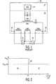
- FIG. 1 illustrates a known lamp ballast 20 for igniting and powering a pair of lamps 10.
- Ballast 20 has a ballast input stage 21 employing an oscillator 22 for driving a ballast output stage 23 having a known arrangement of a tank resonant capacitor C1, a current limiting capacitor C2, and a tank resonant transformer including a primary winding PW1 and secondary windings SW1-SW4.
- a no-load condition i.e., lamps 10 are switched out of ballast 20 or in a pre-ignition phase
- an open circuit voltage across ballast output stage 23 complies with UL requirements.
- ballast output stages 23 of two or more lamp ballasts 20 in series to thereby power additional lamps 10.
- ballast output stages 23 in dependence upon a topology of balance input stages 21, there may be need to limit an open circuit voltage across the series connection of ballast output stages 23 to ensure compliance with UL requirements and any other applicable safety standards.
- the present invention provides an open circuit voltage limiting technique for a series connection of ballast output stages.
- One form of the present invention is a lighting system employing a pair of ballast input stages operable to oscillate at different oscillating frequencies upon an initial powering of the ballast input stages.
- the lighting system further employs a pair of ballast output stages for establishing an open circuit voltage across the ballast output stages in response to an absence of a loading of lamps across the ballast output stages.
- the light system further employ means for, subsequent to the initial powering of the ballast input stages, impeding any parasitic loading across the ballast output stages from phase locking the oscillating frequencies in response to the absence of the loading of the lamps across the ballast output stages.
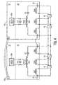
- FIG. 2 the inventor discovered two distinct operation regions 30 and 31 of lamp ballasts 20 (FIG. 1) having a series connection of ballast output stages 23 (FIG. 1) due a sensitivity of oscillator 21 (FIG. 1) to parasitic loading.
- Operation regions 30 and 31 will subsequently be described in the context of a series connection of two (2) output ballast stages 23 to facilitate an understanding of operation regions 30 and 31. From this description, those having ordinary skill in the art will appreciate the how a series connection of three (3) output ballast stages 23 function in the operation regions 30 and 31.
- Operation region 30 is defined by an absolute difference between an oscillating frequency f 1 and an oscillating frequency f 2 of a pair of ballast input stages 21 (FIG. 1) upon initial powering being within a range extending between 0 Hz to a cutoff frequency differential ⁇ f .
- a total rms of an open circuit voltage across the ballast output stages 23 during a no-load condition of the lamps is an open circuit voltage V OC supplied individually by the ballast output stages 23.
- Operation region 31 is defined by the absolute difference between oscillating frequency f 1 and oscillating frequency f 2 of a pair of ballast input stages 21 (FIG. 1) upon initial powering being greater than the cutoff frequency differential ⁇ f .
- total rms of an open circuit voltage across the ballast output stages 23 during a no-load condition of the lamps is less than the open circuit voltage 2V OC by a voltage differential ⁇ V.
- the inventor ascertained that the total rms 2V OC - ⁇ V of the open circuit voltage within operation region 31 resulted from the leakage current from the parasitic loading of the output leads 24, 25 of the series connected ballast output stages 23 being unable to force a phase lock of oscillating frequency f 1 and oscillating frequency f 2 .
- FIGS. 3-6 illustrate various embodiments for implementing the open circuit voltage limiting technique of the present invention for series connected ballast output stages 23.
- FIG. 3 illustrates a version 20a and a version 20b of lamp ballast 20 (FIG. 1) for powering four lamps 10.
- Lamp ballasts 20a and 20b have their ballast input stages 21 coupled in parallel and their ballast output stages 23 coupled in series.
- Ballast input stages 21 employ a pair of self-resonating, free-running oscillators (“SRFRO”) 22a of any type having an absolute oscillating frequency differential greater than zero (0) upon an initial powering of oscillators 22a.
- SRFRO self-resonating, free-running oscillators
- ballast output stage 23 of lamp ballast 20a employs a tank resonant capacitor C1a and ballast output stage 23 of lamp ballast 20b employs a tank resonant capacitor C1b.
- a capacitive differential between capacitors C1a and C1b is chosen to impede any parasitic loading across ballast output stages 23 during a no-load condition of lamps 10 from phase locking the oscillating frequencies of ballast input stages 21.
- the capacitive differential between capacitors C1a and C1b is dependent upon the sensitivity of oscillators 22a to the parasitic loading.
- the inventor is incapable of describing a preferred capacitance differential between capacitors C1a and C1b due to the essentially unlimited number of topologies of oscillators 22a as would be appreciated by those having ordinary skill in the art.
- a minimal capacitance differential between capacitors C1a and C1b can be ascertained by the generation of a beat frequency waveform at no load that shows the oscillating frequencies are not phase locked as would be appreciated by those having ordinary skill in the art.
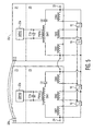
- FIG. 4 illustrates version 20a and a version 20c of lamp ballast 20 (FIG. 1) for powering four lamps 10.
- Lamp ballasts 20a and 20c have their ballast input stages 21 coupled in parallel and their ballast output stages 23 coupled in series.
- Ballast input stages 21 employ a pair of self-resonating, free-running oscillators ("SRFRO") 22a of any type having an absolute oscillating frequency differential greater than zero (0) upon an initial powering of oscillators 22a.
- SRFRO self-resonating, free-running oscillators
- ballast output stage 23 of lamp ballast 20a employs a primary winding PW1a
- ballast output stage 23 of lamp ballast 20b employs a primary winding PW1b.
- a inductive differential between primary windings PW1a and PW1b is chosen to impede any parasitic loading across ballast output stages 23 during a no-load condition of lamps 10 from phase locking the oscillating frequencies of ballast input stages 21.
- the inductive differential between PW1a and PW1b is dependent upon the sensitivity of oscillators 22a to the parasitic loading.
- the inventor is incapable of describing a preferred inductance differential between PW1a and PW1b due to the essentially unlimited number of topologies of oscillators 22a as would be appreciated by those having ordinary skill in the art.
- a minimal inductance differential between PW1a and PW1b can be ascertained by the generation of a beat frequency waveform at no load that shows the oscillating frequencies are not phase locked as would be appreciated by those having ordinary skill in the art.
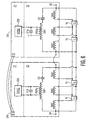
- FIG. 5 illustrates version 20a and a version 20d of lamp ballast 20 (FIG. 1) for powering four lamps 10.
- Lamp ballasts 20a and 20d have their ballast input stages 21 coupled in parallel and their ballast output stages 23 coupled in series.
- Ballast input stages 21 employ a pair of self-resonating, free-running oscillators (“SRFRO”) 22a of any type having an absolute oscillating frequency differential greater than zero (0) upon an initial powering of oscillators 22a.
- SRFRO self-resonating, free-running oscillators
- an air gap between primary winding PW1a and secondary windings SW1-SW4 of lamp ballast 20a is less than the air gap between primary winding PW1a and secondary windings SW1-SW4 of lamp ballast 20d.
- a air gap differential between resonant transformers is chosen to impede any parasitic loading across ballast output stages 23 during a no-load condition of lamps 10 from phase locking the oscillating frequencies of ballast input stages 21.
- the air gap differential between the resonant transformers is dependent upon the sensitivity of oscillators 22a to the parasitic loading.
- the inventor is incapable of describing a preferred air gap differential between the resonant transformers due to the essentially unlimited number of topologies of oscillators 22a as would be appreciated by those having ordinary skill in the art.
- a minimal air gap differential between the resonant transformers can be ascertained by the generation of a beat frequency waveform at no load that shows the oscillating frequencies are not phase locked as would be appreciated by those having ordinary skill in the art.
- FIG. 6 illustrates a version 20e and a version 20f of lamp ballast 20 (FIG. 1) for powering four lamps 10.
- Lamp ballasts 20e and 20f have their input stages 21 coupled in parallel and their output stages 23 coupled in series.
- Lamp ballasts 20ae and 20f both employ a digitally controlled oscillator (“DSCO") 22b of any type.
- the oscillators 22b are programmed to maintain an oscillating frequency differential between the oscillators 22b upon and subsequent to the powering of ballast input stages 21.
- the oscillating frequency differential is chosen to impede any parasitic loading across ballast output stages 23 during a no-load condition of lamps 10 from phase locking the oscillating frequencies of ballast input stages 21.
- the oscillating frequency differential is dependent upon the sensitivity of oscillators 22b to the parasitic loading.
- the inventor is incapable of describing a preferred oscillating frequency differential due to the essentially unlimited number of topologies of oscillators 22b as would be appreciated by those having ordinary skill in the art.
- a minimal oscillating frequency differential can be ascertained by the generation of a beat frequency waveform at no load that shows the oscillating frequencies are not phase locked as would be appreciated by those having ordinary skill in the art.
Landscapes
- Engineering & Computer Science (AREA)
- Power Engineering (AREA)
- Circuit Arrangements For Discharge Lamps (AREA)
- Circuit Arrangement For Electric Light Sources In General (AREA)
Claims (5)
- Système d'éclairage comprenant :- un premier étage d'entrée de ballast (21) et un deuxième étage d'entrée de ballast (21), ledit premier étage d'entrée de ballast (21) pouvant fonctionner pour osciller à une première fréquence d'oscillations (f 1) et ledit deuxième étage d'entrée de ballast (21) pouvant fonctionner pour osciller à une deuxième fréquence d'oscillation (f 2), la première fréquence d'oscillation (f 1) et la deuxième fréquence d'oscillation (f 2) étant dissemblables lors de l'alimentation initiale dudit premier étage d'entrée de ballast (21) et dudit deuxième étage d'entrée de ballast (21);- un premier étage de sortie de ballast (23) et un deuxième étage de sortie de ballast (23) raccordés en série, ledit premier étage de sortie de ballast (23) en communication électrique avec ledit premier étage de ballast (21) et ledit deuxième étage de sortie de ballast (23) en communication électrique avec ledit deuxième étage de ballast (21) pour établir une tension de circuit ouvert aux bornes dudit premier étage de sortie de ballast (23) et dudit deuxième étage de sortie de ballast (23) en réponse à une absence d'une charge d'une pluralité de lampes (10) aux bornes dudit premier étage de sortie de ballast (23) et dudit deuxième étage de sortie de ballast (23); et- un moyen pour, consécutivement à l'alimentation initiale dudit premier étage d'entrée de ballast (21) et dudit deuxième étage d'entrée de ballast (21) et en réponse à l'absence de la charge par la pluralité de lampes (10) aux bornes dudit premier étage de sortie de ballast (23) et dudit deuxième étage de sortie de ballast (23), empêcher toute charge parasite aux bornes dudit premier étage de sortie de ballast (23) et dudit deuxième étage de sortie de ballast (23) de mettre en verrouillage de phase la première fréquence d'oscillation (f 1) et la deuxième fréquence d'oscillation (f 2).
- Système d'éclairage selon la revendication 1,
dans lequel ledit premier étage de sortie de ballast (23) inclut un premier condensateur résonnant d'oscillateur (C1a);
dans lequel ledit deuxième étage de sortie de ballast (23) inclut un deuxième condensateur résonnant d'oscillateur (C1b); et
dans lequel, consécutivement à l'alimentation initiale dudit premier étage d'entrée de ballast (21) et dudit deuxième étage d'entrée de ballast (21) et en réponse à l'absence de charge de la pluralité de lampes (10) aux bornes dudit premier étage de sortie de ballast (23) et dudit deuxième étage de sortie de ballast (23), un différentiel de capacité entre ledit premier condensateur résonnant d'oscillateur (C1a) et ledit deuxième condensateur résonnant d'oscillateur (C1b) empêche toute charge parasite aux bornes dudit premier étage de sortie de ballast (23) et dudit deuxième étage de sortie de ballast (23) de mettre en verrouillage de phase la première fréquence d'oscillation (f 1) et la deuxième fréquence d'oscillation (f 2). - Système d'éclairage selon la revendication 1,
dans lequel ledit premier étage de sortie de ballast (23) inclut un premier enroulement primaire (PW1a);
dans lequel ledit deuxième étage de sortie de ballast (23) inclut un deuxième enroulement primaire (PW1b); et
dans lequel, consécutivement à l'alimentation initiale dudit premier étage d'entrée de ballast (21) et dudit deuxième étage d'entrée de ballast (21) et en réponse à l'absence de la charge de la pluralité de lampes (10) aux bornes dudit premier étage de sortie de ballast (23) et dudit deuxième étage de sortie de ballast (23), un différentiel inductif entre ledit premier enroulement primaire (PW1a) et ledit deuxième enroulement primaire (PW1b) empêche toute charge parasite aux bornes dudit premier étage de sortie de ballast (23) et dudit deuxième étage de sortie (23) de mettre en verrouillage de phase la première fréquence d'oscillation (f 1) et la deuxième fréquence d'oscillation (f 2). - Système d'éclairage selon la revendication 1,
dans lequel ledit premier étage de sortie de ballast (23) inclut un premier enroulement (PW1a) et un premier au moins un enroulement secondaire (SW1-SW4) espacé dudit premier enroulement primaire (PW1a) par un premier intervalle d'air;
dans lequel ledit deuxième étage de sortie (23) inclut un deuxième enroulement primaire (PW1b) et un deuxième au moins un enroulement secondaire (SW1-SW4) espacé dudit premier enroulement primaire (PW1a) par un intervalle d'air; et
dans lequel, consécutivement à l'alimentation initiale dudit premier étage d'entrée de ballast (21) et dudit deuxième étage d'entrée de ballast (21) et en réponse à l'absence de la charge de la pluralité de lampes (10) aux bornes dudit premier étage de sortie de ballast (23) et dudit deuxième étage de sortie de ballast (23), un différentiel entre le premier intervalle d'air et le deuxième intervalle d'air empêche toute charge parasite aux bornes dudit premier étage de sortie de ballast (23) et dudit deuxième étage de sortie de ballast (23) de mettre en verrouillage de phase la première fréquence d'oscillation (f 1) et la deuxième fréquence d'oscillation (f 2). - Système d'éclairage selon la revendication 1,
dans lequel ledit premier étage de sortie de ballast (23) inclut un premier oscillateur (22b) fonctionnant à une première fréquence d'oscillation (f 1);
dans lequel ledit deuxième étage de sortie de ballast (23) inclut un deuxième oscillateur (22b) fonctionnant à une deuxième fréquence d'oscillation (f 2); et
dans lequel, consécutivement à l'alimentation initiale dudit premier étage d'entrée de ballast (21) et dudit deuxième étage d'entrée de ballast (21) et en réponse à l'absence de la charge de la pluralité de lampes (10) aux bornes dudit premier étage de sortie de ballast (23) et dudit deuxième étage de sortie de ballast (23), un différentiel entre la première fréquence d'oscillation (f 1) et la deuxième fréquence d'oscillation (f 2) est conservé par ledit premier oscillateur (22b) et par ledit deuxième oscillateur (22b) pour empêcher toute charge parasite aux bornes dudit premier étage de sortie de ballast (23) et dudit deuxième étage de sortie de ballast (23) de mettre en verrouillage de phase la première fréquence d'oscillation (f 1) et la deuxième fréquence d'oscillation (f 2).
Applications Claiming Priority (2)
| Application Number | Priority Date | Filing Date | Title |
|---|---|---|---|
| US47170103P | 2003-05-19 | 2003-05-19 | |
| PCT/IB2004/001588 WO2004103031A1 (fr) | 2003-05-19 | 2004-05-10 | Ballast a tension de circuit ouvert limitee |
Publications (2)
| Publication Number | Publication Date |
|---|---|
| EP1627557A1 EP1627557A1 (fr) | 2006-02-22 |
| EP1627557B1 true EP1627557B1 (fr) | 2007-07-04 |
Family
ID=33452455
Family Applications (1)
| Application Number | Title | Priority Date | Filing Date |
|---|---|---|---|
| EP04731976A Expired - Lifetime EP1627557B1 (fr) | 2003-05-19 | 2004-05-10 | Ballast a tension de circuit ouvert limitee |
Country Status (7)
| Country | Link |
|---|---|
| US (1) | US7239092B2 (fr) |
| EP (1) | EP1627557B1 (fr) |
| JP (1) | JP2006529051A (fr) |
| CN (1) | CN1792121A (fr) |
| AT (1) | ATE366507T1 (fr) |
| DE (1) | DE602004007384T2 (fr) |
| WO (1) | WO2004103031A1 (fr) |
Families Citing this family (3)
| Publication number | Priority date | Publication date | Assignee | Title |
|---|---|---|---|---|
| US20060037018A1 (en) * | 2004-08-16 | 2006-02-16 | Dell Products L.P. | System, method and software providing an adaptive job dispatch algorithm for large distributed jobs |
| DE102006062205B4 (de) * | 2006-08-25 | 2012-07-19 | Minebea Co., Ltd. | Hochspannungstransformator |
| US8274239B2 (en) | 2010-06-09 | 2012-09-25 | General Electric Company | Open circuit voltage clamp for electronic HID ballast |
Family Cites Families (14)
| Publication number | Priority date | Publication date | Assignee | Title |
|---|---|---|---|---|
| US4819146A (en) * | 1986-10-10 | 1989-04-04 | Nilssen Ole K | Resonant inverter having frequency control |
| US5512801A (en) * | 1980-08-14 | 1996-04-30 | Nilssen; Ole K. | Ballast for instant-start parallel-connected lamps |
| US5216332A (en) * | 1982-08-25 | 1993-06-01 | Nilssen Ole K | Magnetic-electronic ballast for fluorescent lamps |
| US5270618A (en) * | 1987-01-09 | 1993-12-14 | Nilssen Ole K | Magnetic-electronic dual-frequency ballast |
| US4902942A (en) * | 1988-06-02 | 1990-02-20 | General Electric Company | Controlled leakage transformer for fluorescent lamp ballast including integral ballasting inductor |
| US5115347A (en) * | 1990-08-20 | 1992-05-19 | Nilssen Ole K | Electronically power-factor-corrected ballast |
| US5117158A (en) * | 1991-02-04 | 1992-05-26 | Abe Arbel | Electronic ballast for fluorescent lights |
| US6121733A (en) * | 1991-06-10 | 2000-09-19 | Nilssen; Ole K. | Controlled inverter-type fluorescent lamp ballast |
| US6181085B1 (en) * | 1995-02-22 | 2001-01-30 | Ole K. Nilssen | Electronic ballast with output control feature |
| US6072282A (en) * | 1997-12-02 | 2000-06-06 | Power Circuit Innovations, Inc. | Frequency controlled quick and soft start gas discharge lamp ballast and method therefor |
| US5925990A (en) * | 1997-12-19 | 1999-07-20 | Energy Savings, Inc. | Microprocessor controlled electronic ballast |
| US6194840B1 (en) * | 1998-12-28 | 2001-02-27 | Philips Electronics North America Corporation | Self-oscillating resonant converter with passive filter regulator |
| DE10244412A1 (de) * | 2001-09-25 | 2003-05-28 | Toshiba Lighting & Technology | Elektronisches Vorschaltgerät und Leuchte |
| US6667585B2 (en) * | 2002-02-20 | 2003-12-23 | Northrop Grumman Corporation | Fluorescent lamp brightness control process by ballast frequency adjustment |
-
2004
- 2004-05-10 US US10/557,976 patent/US7239092B2/en not_active Expired - Fee Related
- 2004-05-10 AT AT04731976T patent/ATE366507T1/de not_active IP Right Cessation
- 2004-05-10 CN CNA2004800136858A patent/CN1792121A/zh active Pending
- 2004-05-10 JP JP2006530657A patent/JP2006529051A/ja not_active Withdrawn
- 2004-05-10 EP EP04731976A patent/EP1627557B1/fr not_active Expired - Lifetime
- 2004-05-10 WO PCT/IB2004/001588 patent/WO2004103031A1/fr not_active Ceased
- 2004-05-10 DE DE602004007384T patent/DE602004007384T2/de not_active Expired - Fee Related
Also Published As
| Publication number | Publication date |
|---|---|
| CN1792121A (zh) | 2006-06-21 |
| WO2004103031A1 (fr) | 2004-11-25 |
| US20060261758A1 (en) | 2006-11-23 |
| JP2006529051A (ja) | 2006-12-28 |
| US7239092B2 (en) | 2007-07-03 |
| ATE366507T1 (de) | 2007-07-15 |
| DE602004007384D1 (de) | 2007-08-16 |
| EP1627557A1 (fr) | 2006-02-22 |
| DE602004007384T2 (de) | 2008-03-06 |
Similar Documents
| Publication | Publication Date | Title |
|---|---|---|
| US6534934B1 (en) | Multi-lamp driving system | |
| FI69740B (fi) | Foerkopplingsanordning foer anvaendning vid laogtrycksurladdningslampor | |
| US4782268A (en) | Low-pressure discharge lamp, particularly fluorescent lamp high-frequency operating circuit with low-power network interference | |
| EP1330943B1 (fr) | Onduleur de ballast auto-oscillant a retroaction de tension commandee en phase | |
| EP1814367B1 (fr) | Onduleur de retroeclairage et son procede d'attaque | |
| US6069455A (en) | Ballast having a selectively resonant circuit | |
| FI111791B (fi) | Liitäntälaite vähintään yhdelle rinnankäyttöiselle kaasupurkauslamppuparille | |
| US5677601A (en) | Operating circuit for low-power low-pressure discharge lamps, particularly compact fluorescent lamps | |
| WO2009029334A2 (fr) | Limitation thermique pour ballasts de lampe fluorescente linéaire | |
| EP1627557B1 (fr) | Ballast a tension de circuit ouvert limitee | |
| EP1464208A1 (fr) | Dispositif de circuit pour faire fonctionner une ou plusieurs lampes | |
| WO2006082849A1 (fr) | Dispositif de mise en oeuvre de lampe a decharge | |
| KR100427466B1 (ko) | 방전등 점등 장치 | |
| US6861811B2 (en) | Half bridge with constant amplitude drive signal | |
| JP2006012660A (ja) | 放電灯点灯回路 | |
| US7304441B2 (en) | Method and apparatus for driving discharge lamps in a floating configuration | |
| JP2006012659A (ja) | 放電灯点灯回路 | |
| KR960006610B1 (ko) | 방전등용 전자식 안정기의 점등회로 | |
| KR100848758B1 (ko) | 방전등 점등 장치 | |
| JPH048915B2 (fr) | ||
| US5818176A (en) | Circuit arrangement for the operation of discharge lamps | |
| US20110291579A1 (en) | Discharge lamp starting circuit and discharge lamp lighting device | |
| JP2009054413A (ja) | 放電灯点灯装置 | |
| JPH02162699A (ja) | 放電灯点灯装置 | |
| JP2000021585A (ja) | ギャップ付き電流トランスによる高周波定電流蛍光灯 点灯方式 |
Legal Events
| Date | Code | Title | Description |
|---|---|---|---|
| PUAI | Public reference made under article 153(3) epc to a published international application that has entered the european phase |
Free format text: ORIGINAL CODE: 0009012 |
|
| 17P | Request for examination filed |
Effective date: 20051219 |
|
| AK | Designated contracting states |
Kind code of ref document: A1 Designated state(s): AT BE BG CH CY CZ DE DK EE ES FI FR GB GR HU IE IT LI LU MC NL PL PT RO SE SI SK TR |
|
| DAX | Request for extension of the european patent (deleted) | ||
| GRAP | Despatch of communication of intention to grant a patent |
Free format text: ORIGINAL CODE: EPIDOSNIGR1 |
|
| GRAS | Grant fee paid |
Free format text: ORIGINAL CODE: EPIDOSNIGR3 |
|
| GRAA | (expected) grant |
Free format text: ORIGINAL CODE: 0009210 |
|
| AK | Designated contracting states |
Kind code of ref document: B1 Designated state(s): AT BE BG CH CY CZ DE DK EE ES FI FR GB GR HU IE IT LI LU MC NL PL PT RO SE SI SK TR |
|
| REG | Reference to a national code |
Ref country code: GB Ref legal event code: FG4D |
|
| REG | Reference to a national code |
Ref country code: CH Ref legal event code: EP |
|
| REG | Reference to a national code |
Ref country code: IE Ref legal event code: FG4D |
|
| REF | Corresponds to: |
Ref document number: 602004007384 Country of ref document: DE Date of ref document: 20070816 Kind code of ref document: P |
|
| REG | Reference to a national code |
Ref country code: GB Ref legal event code: 746 Effective date: 20070916 |
|
| ET | Fr: translation filed | ||
| NLV1 | Nl: lapsed or annulled due to failure to fulfill the requirements of art. 29p and 29m of the patents act | ||
| REG | Reference to a national code |
Ref country code: CH Ref legal event code: PL |
|
| PG25 | Lapsed in a contracting state [announced via postgrant information from national office to epo] |
Ref country code: SI Free format text: LAPSE BECAUSE OF FAILURE TO SUBMIT A TRANSLATION OF THE DESCRIPTION OR TO PAY THE FEE WITHIN THE PRESCRIBED TIME-LIMIT Effective date: 20070704 Ref country code: BG Free format text: LAPSE BECAUSE OF FAILURE TO SUBMIT A TRANSLATION OF THE DESCRIPTION OR TO PAY THE FEE WITHIN THE PRESCRIBED TIME-LIMIT Effective date: 20071004 Ref country code: NL Free format text: LAPSE BECAUSE OF FAILURE TO SUBMIT A TRANSLATION OF THE DESCRIPTION OR TO PAY THE FEE WITHIN THE PRESCRIBED TIME-LIMIT Effective date: 20070704 Ref country code: ES Free format text: LAPSE BECAUSE OF FAILURE TO SUBMIT A TRANSLATION OF THE DESCRIPTION OR TO PAY THE FEE WITHIN THE PRESCRIBED TIME-LIMIT Effective date: 20071015 Ref country code: PT Free format text: LAPSE BECAUSE OF FAILURE TO SUBMIT A TRANSLATION OF THE DESCRIPTION OR TO PAY THE FEE WITHIN THE PRESCRIBED TIME-LIMIT Effective date: 20071204 Ref country code: FI Free format text: LAPSE BECAUSE OF FAILURE TO SUBMIT A TRANSLATION OF THE DESCRIPTION OR TO PAY THE FEE WITHIN THE PRESCRIBED TIME-LIMIT Effective date: 20070704 |
|
| PG25 | Lapsed in a contracting state [announced via postgrant information from national office to epo] |
Ref country code: AT Free format text: LAPSE BECAUSE OF FAILURE TO SUBMIT A TRANSLATION OF THE DESCRIPTION OR TO PAY THE FEE WITHIN THE PRESCRIBED TIME-LIMIT Effective date: 20070704 Ref country code: PL Free format text: LAPSE BECAUSE OF FAILURE TO SUBMIT A TRANSLATION OF THE DESCRIPTION OR TO PAY THE FEE WITHIN THE PRESCRIBED TIME-LIMIT Effective date: 20070704 Ref country code: LI Free format text: LAPSE BECAUSE OF FAILURE TO SUBMIT A TRANSLATION OF THE DESCRIPTION OR TO PAY THE FEE WITHIN THE PRESCRIBED TIME-LIMIT Effective date: 20070704 Ref country code: CH Free format text: LAPSE BECAUSE OF FAILURE TO SUBMIT A TRANSLATION OF THE DESCRIPTION OR TO PAY THE FEE WITHIN THE PRESCRIBED TIME-LIMIT Effective date: 20070704 |
|
| PG25 | Lapsed in a contracting state [announced via postgrant information from national office to epo] |
Ref country code: BE Free format text: LAPSE BECAUSE OF FAILURE TO SUBMIT A TRANSLATION OF THE DESCRIPTION OR TO PAY THE FEE WITHIN THE PRESCRIBED TIME-LIMIT Effective date: 20070704 |
|
| PG25 | Lapsed in a contracting state [announced via postgrant information from national office to epo] |
Ref country code: GR Free format text: LAPSE BECAUSE OF FAILURE TO SUBMIT A TRANSLATION OF THE DESCRIPTION OR TO PAY THE FEE WITHIN THE PRESCRIBED TIME-LIMIT Effective date: 20071005 Ref country code: DK Free format text: LAPSE BECAUSE OF FAILURE TO SUBMIT A TRANSLATION OF THE DESCRIPTION OR TO PAY THE FEE WITHIN THE PRESCRIBED TIME-LIMIT Effective date: 20070704 |
|
| PLBE | No opposition filed within time limit |
Free format text: ORIGINAL CODE: 0009261 |
|
| STAA | Information on the status of an ep patent application or granted ep patent |
Free format text: STATUS: NO OPPOSITION FILED WITHIN TIME LIMIT |
|
| PG25 | Lapsed in a contracting state [announced via postgrant information from national office to epo] |
Ref country code: CZ Free format text: LAPSE BECAUSE OF FAILURE TO SUBMIT A TRANSLATION OF THE DESCRIPTION OR TO PAY THE FEE WITHIN THE PRESCRIBED TIME-LIMIT Effective date: 20070704 Ref country code: SK Free format text: LAPSE BECAUSE OF FAILURE TO SUBMIT A TRANSLATION OF THE DESCRIPTION OR TO PAY THE FEE WITHIN THE PRESCRIBED TIME-LIMIT Effective date: 20070704 |
|
| 26N | No opposition filed |
Effective date: 20080407 |
|
| PG25 | Lapsed in a contracting state [announced via postgrant information from national office to epo] |
Ref country code: SE Free format text: LAPSE BECAUSE OF FAILURE TO SUBMIT A TRANSLATION OF THE DESCRIPTION OR TO PAY THE FEE WITHIN THE PRESCRIBED TIME-LIMIT Effective date: 20071004 Ref country code: RO Free format text: LAPSE BECAUSE OF FAILURE TO SUBMIT A TRANSLATION OF THE DESCRIPTION OR TO PAY THE FEE WITHIN THE PRESCRIBED TIME-LIMIT Effective date: 20070704 |
|
| PGFP | Annual fee paid to national office [announced via postgrant information from national office to epo] |
Ref country code: DE Payment date: 20080716 Year of fee payment: 5 |
|
| PGFP | Annual fee paid to national office [announced via postgrant information from national office to epo] |
Ref country code: FR Payment date: 20080528 Year of fee payment: 5 |
|
| PG25 | Lapsed in a contracting state [announced via postgrant information from national office to epo] |
Ref country code: MC Free format text: LAPSE BECAUSE OF NON-PAYMENT OF DUE FEES Effective date: 20080531 |
|
| PGFP | Annual fee paid to national office [announced via postgrant information from national office to epo] |
Ref country code: GB Payment date: 20080616 Year of fee payment: 5 |
|
| PG25 | Lapsed in a contracting state [announced via postgrant information from national office to epo] |
Ref country code: EE Free format text: LAPSE BECAUSE OF FAILURE TO SUBMIT A TRANSLATION OF THE DESCRIPTION OR TO PAY THE FEE WITHIN THE PRESCRIBED TIME-LIMIT Effective date: 20070704 |
|
| PG25 | Lapsed in a contracting state [announced via postgrant information from national office to epo] |
Ref country code: IE Free format text: LAPSE BECAUSE OF NON-PAYMENT OF DUE FEES Effective date: 20080512 |
|
| PG25 | Lapsed in a contracting state [announced via postgrant information from national office to epo] |
Ref country code: CY Free format text: LAPSE BECAUSE OF FAILURE TO SUBMIT A TRANSLATION OF THE DESCRIPTION OR TO PAY THE FEE WITHIN THE PRESCRIBED TIME-LIMIT Effective date: 20070704 |
|
| GBPC | Gb: european patent ceased through non-payment of renewal fee |
Effective date: 20090510 |
|
| REG | Reference to a national code |
Ref country code: FR Ref legal event code: ST Effective date: 20100129 |
|
| PG25 | Lapsed in a contracting state [announced via postgrant information from national office to epo] |
Ref country code: FR Free format text: LAPSE BECAUSE OF NON-PAYMENT OF DUE FEES Effective date: 20090602 |
|
| PG25 | Lapsed in a contracting state [announced via postgrant information from national office to epo] |
Ref country code: GB Free format text: LAPSE BECAUSE OF NON-PAYMENT OF DUE FEES Effective date: 20090510 |
|
| PG25 | Lapsed in a contracting state [announced via postgrant information from national office to epo] |
Ref country code: DE Free format text: LAPSE BECAUSE OF NON-PAYMENT OF DUE FEES Effective date: 20091201 |
|
| PG25 | Lapsed in a contracting state [announced via postgrant information from national office to epo] |
Ref country code: LU Free format text: LAPSE BECAUSE OF NON-PAYMENT OF DUE FEES Effective date: 20080510 Ref country code: HU Free format text: LAPSE BECAUSE OF FAILURE TO SUBMIT A TRANSLATION OF THE DESCRIPTION OR TO PAY THE FEE WITHIN THE PRESCRIBED TIME-LIMIT Effective date: 20080105 |
|
| PG25 | Lapsed in a contracting state [announced via postgrant information from national office to epo] |
Ref country code: TR Free format text: LAPSE BECAUSE OF FAILURE TO SUBMIT A TRANSLATION OF THE DESCRIPTION OR TO PAY THE FEE WITHIN THE PRESCRIBED TIME-LIMIT Effective date: 20070704 |
|
| PG25 | Lapsed in a contracting state [announced via postgrant information from national office to epo] |
Ref country code: IT Free format text: LAPSE BECAUSE OF NON-PAYMENT OF DUE FEES Effective date: 20080531 |