EP1629543B1 - Films barrieres pour substrats polymers flexibles fabriques par depot de couches atomiques - Google Patents
Films barrieres pour substrats polymers flexibles fabriques par depot de couches atomiques Download PDFInfo
- Publication number
- EP1629543B1 EP1629543B1 EP04785558.0A EP04785558A EP1629543B1 EP 1629543 B1 EP1629543 B1 EP 1629543B1 EP 04785558 A EP04785558 A EP 04785558A EP 1629543 B1 EP1629543 B1 EP 1629543B1
- Authority
- EP
- European Patent Office
- Prior art keywords
- article
- substrate
- barrier
- nanometers
- atomic layer
- Prior art date
- Legal status (The legal status is an assumption and is not a legal conclusion. Google has not performed a legal analysis and makes no representation as to the accuracy of the status listed.)
- Revoked
Links
Images


Classifications
-
- H—ELECTRICITY
- H10—SEMICONDUCTOR DEVICES; ELECTRIC SOLID-STATE DEVICES NOT OTHERWISE PROVIDED FOR
- H10K—ORGANIC ELECTRIC SOLID-STATE DEVICES
- H10K50/00—Organic light-emitting devices
- H10K50/80—Constructional details
- H10K50/84—Passivation; Containers; Encapsulations
- H10K50/844—Encapsulations
-
- C—CHEMISTRY; METALLURGY
- C23—COATING METALLIC MATERIAL; COATING MATERIAL WITH METALLIC MATERIAL; CHEMICAL SURFACE TREATMENT; DIFFUSION TREATMENT OF METALLIC MATERIAL; COATING BY VACUUM EVAPORATION, BY SPUTTERING, BY ION IMPLANTATION OR BY CHEMICAL VAPOUR DEPOSITION, IN GENERAL; INHIBITING CORROSION OF METALLIC MATERIAL OR INCRUSTATION IN GENERAL
- C23C—COATING METALLIC MATERIAL; COATING MATERIAL WITH METALLIC MATERIAL; SURFACE TREATMENT OF METALLIC MATERIAL BY DIFFUSION INTO THE SURFACE, BY CHEMICAL CONVERSION OR SUBSTITUTION; COATING BY VACUUM EVAPORATION, BY SPUTTERING, BY ION IMPLANTATION OR BY CHEMICAL VAPOUR DEPOSITION, IN GENERAL
- C23C16/00—Chemical coating by decomposition of gaseous compounds, without leaving reaction products of surface material in the coating, i.e. chemical vapour deposition [CVD] processes
- C23C16/22—Chemical coating by decomposition of gaseous compounds, without leaving reaction products of surface material in the coating, i.e. chemical vapour deposition [CVD] processes characterised by the deposition of inorganic material, other than metallic material
- C23C16/30—Deposition of compounds, mixtures or solid solutions, e.g. borides, carbides, nitrides
- C23C16/40—Oxides
- C23C16/403—Oxides of aluminium, magnesium or beryllium
-
- C—CHEMISTRY; METALLURGY
- C23—COATING METALLIC MATERIAL; COATING MATERIAL WITH METALLIC MATERIAL; CHEMICAL SURFACE TREATMENT; DIFFUSION TREATMENT OF METALLIC MATERIAL; COATING BY VACUUM EVAPORATION, BY SPUTTERING, BY ION IMPLANTATION OR BY CHEMICAL VAPOUR DEPOSITION, IN GENERAL; INHIBITING CORROSION OF METALLIC MATERIAL OR INCRUSTATION IN GENERAL
- C23C—COATING METALLIC MATERIAL; COATING MATERIAL WITH METALLIC MATERIAL; SURFACE TREATMENT OF METALLIC MATERIAL BY DIFFUSION INTO THE SURFACE, BY CHEMICAL CONVERSION OR SUBSTITUTION; COATING BY VACUUM EVAPORATION, BY SPUTTERING, BY ION IMPLANTATION OR BY CHEMICAL VAPOUR DEPOSITION, IN GENERAL
- C23C16/00—Chemical coating by decomposition of gaseous compounds, without leaving reaction products of surface material in the coating, i.e. chemical vapour deposition [CVD] processes
- C23C16/44—Chemical coating by decomposition of gaseous compounds, without leaving reaction products of surface material in the coating, i.e. chemical vapour deposition [CVD] processes characterised by the method of coating
- C23C16/455—Chemical coating by decomposition of gaseous compounds, without leaving reaction products of surface material in the coating, i.e. chemical vapour deposition [CVD] processes characterised by the method of coating characterised by the method used for introducing gases into reaction chamber or for modifying gas flows in reaction chamber
- C23C16/45523—Pulsed gas flow or change of composition over time
- C23C16/45525—Atomic layer deposition [ALD]
-
- C—CHEMISTRY; METALLURGY
- C23—COATING METALLIC MATERIAL; COATING MATERIAL WITH METALLIC MATERIAL; CHEMICAL SURFACE TREATMENT; DIFFUSION TREATMENT OF METALLIC MATERIAL; COATING BY VACUUM EVAPORATION, BY SPUTTERING, BY ION IMPLANTATION OR BY CHEMICAL VAPOUR DEPOSITION, IN GENERAL; INHIBITING CORROSION OF METALLIC MATERIAL OR INCRUSTATION IN GENERAL
- C23C—COATING METALLIC MATERIAL; COATING MATERIAL WITH METALLIC MATERIAL; SURFACE TREATMENT OF METALLIC MATERIAL BY DIFFUSION INTO THE SURFACE, BY CHEMICAL CONVERSION OR SUBSTITUTION; COATING BY VACUUM EVAPORATION, BY SPUTTERING, BY ION IMPLANTATION OR BY CHEMICAL VAPOUR DEPOSITION, IN GENERAL
- C23C16/00—Chemical coating by decomposition of gaseous compounds, without leaving reaction products of surface material in the coating, i.e. chemical vapour deposition [CVD] processes
- C23C16/44—Chemical coating by decomposition of gaseous compounds, without leaving reaction products of surface material in the coating, i.e. chemical vapour deposition [CVD] processes characterised by the method of coating
- C23C16/455—Chemical coating by decomposition of gaseous compounds, without leaving reaction products of surface material in the coating, i.e. chemical vapour deposition [CVD] processes characterised by the method of coating characterised by the method used for introducing gases into reaction chamber or for modifying gas flows in reaction chamber
- C23C16/45523—Pulsed gas flow or change of composition over time
- C23C16/45525—Atomic layer deposition [ALD]
- C23C16/45555—Atomic layer deposition [ALD] applied in non-semiconductor technology
-
- H—ELECTRICITY
- H10—SEMICONDUCTOR DEVICES; ELECTRIC SOLID-STATE DEVICES NOT OTHERWISE PROVIDED FOR
- H10K—ORGANIC ELECTRIC SOLID-STATE DEVICES
- H10K50/00—Organic light-emitting devices
- H10K50/10—OLEDs or polymer light-emitting diodes [PLED]
- H10K50/11—OLEDs or polymer light-emitting diodes [PLED] characterised by the electroluminescent [EL] layers
- H10K50/125—OLEDs or polymer light-emitting diodes [PLED] characterised by the electroluminescent [EL] layers specially adapted for multicolour light emission, e.g. for emitting white light
- H10K50/13—OLEDs or polymer light-emitting diodes [PLED] characterised by the electroluminescent [EL] layers specially adapted for multicolour light emission, e.g. for emitting white light comprising stacked EL layers within one EL unit
-
- H—ELECTRICITY
- H10—SEMICONDUCTOR DEVICES; ELECTRIC SOLID-STATE DEVICES NOT OTHERWISE PROVIDED FOR
- H10K—ORGANIC ELECTRIC SOLID-STATE DEVICES
- H10K77/00—Constructional details of devices covered by this subclass and not covered by groups H10K10/80, H10K30/80, H10K50/80 or H10K59/80
- H10K77/10—Substrates, e.g. flexible substrates
-
- H—ELECTRICITY
- H10—SEMICONDUCTOR DEVICES; ELECTRIC SOLID-STATE DEVICES NOT OTHERWISE PROVIDED FOR
- H10P—GENERIC PROCESSES OR APPARATUS FOR THE MANUFACTURE OR TREATMENT OF DEVICES COVERED BY CLASS H10
- H10P14/00—Formation of materials, e.g. in the shape of layers or pillars
- H10P14/60—Formation of materials, e.g. in the shape of layers or pillars of insulating materials
- H10P14/63—Formation of materials, e.g. in the shape of layers or pillars of insulating materials characterised by the formation processes
- H10P14/6326—Deposition processes
- H10P14/6328—Deposition from the gas or vapour phase
- H10P14/6334—Deposition from the gas or vapour phase using decomposition or reaction of gaseous or vapour phase compounds, i.e. chemical vapour deposition
- H10P14/6339—Deposition from the gas or vapour phase using decomposition or reaction of gaseous or vapour phase compounds, i.e. chemical vapour deposition deposition by cyclic CVD, e.g. ALD, ALE or pulsed CVD
-
- H—ELECTRICITY
- H10—SEMICONDUCTOR DEVICES; ELECTRIC SOLID-STATE DEVICES NOT OTHERWISE PROVIDED FOR
- H10P—GENERIC PROCESSES OR APPARATUS FOR THE MANUFACTURE OR TREATMENT OF DEVICES COVERED BY CLASS H10
- H10P14/00—Formation of materials, e.g. in the shape of layers or pillars
- H10P14/60—Formation of materials, e.g. in the shape of layers or pillars of insulating materials
- H10P14/69—Inorganic materials
- H10P14/692—Inorganic materials composed of oxides, glassy oxides or oxide-based glasses
- H10P14/6938—Inorganic materials composed of oxides, glassy oxides or oxide-based glasses the material containing at least one metal element, e.g. metal oxides, metal oxynitrides or metal oxycarbides
- H10P14/6939—Inorganic materials composed of oxides, glassy oxides or oxide-based glasses the material containing at least one metal element, e.g. metal oxides, metal oxynitrides or metal oxycarbides characterised by the metal
- H10P14/69391—Inorganic materials composed of oxides, glassy oxides or oxide-based glasses the material containing at least one metal element, e.g. metal oxides, metal oxynitrides or metal oxycarbides characterised by the metal the material containing aluminium, e.g. Al2O3
-
- H—ELECTRICITY
- H10—SEMICONDUCTOR DEVICES; ELECTRIC SOLID-STATE DEVICES NOT OTHERWISE PROVIDED FOR
- H10W—GENERIC PACKAGES, INTERCONNECTIONS, CONNECTORS OR OTHER CONSTRUCTIONAL DETAILS OF DEVICES COVERED BY CLASS H10
- H10W42/00—Arrangements for protection of devices
-
- G—PHYSICS
- G02—OPTICS
- G02F—OPTICAL DEVICES OR ARRANGEMENTS FOR THE CONTROL OF LIGHT BY MODIFICATION OF THE OPTICAL PROPERTIES OF THE MEDIA OF THE ELEMENTS INVOLVED THEREIN; NON-LINEAR OPTICS; FREQUENCY-CHANGING OF LIGHT; OPTICAL LOGIC ELEMENTS; OPTICAL ANALOGUE/DIGITAL CONVERTERS
- G02F1/00—Devices or arrangements for the control of the intensity, colour, phase, polarisation or direction of light arriving from an independent light source, e.g. switching, gating or modulating; Non-linear optics
- G02F1/01—Devices or arrangements for the control of the intensity, colour, phase, polarisation or direction of light arriving from an independent light source, e.g. switching, gating or modulating; Non-linear optics for the control of the intensity, phase, polarisation or colour
- G02F1/13—Devices or arrangements for the control of the intensity, colour, phase, polarisation or direction of light arriving from an independent light source, e.g. switching, gating or modulating; Non-linear optics for the control of the intensity, phase, polarisation or colour based on liquid crystals, e.g. single liquid crystal display cells
- G02F1/133—Constructional arrangements; Operation of liquid crystal cells; Circuit arrangements
- G02F1/1333—Constructional arrangements; Manufacturing methods
- G02F1/133345—Insulating layers
-
- H—ELECTRICITY
- H10—SEMICONDUCTOR DEVICES; ELECTRIC SOLID-STATE DEVICES NOT OTHERWISE PROVIDED FOR
- H10K—ORGANIC ELECTRIC SOLID-STATE DEVICES
- H10K30/00—Organic devices sensitive to infrared radiation, light, electromagnetic radiation of shorter wavelength or corpuscular radiation
- H10K30/50—Photovoltaic [PV] devices
-
- Y—GENERAL TAGGING OF NEW TECHNOLOGICAL DEVELOPMENTS; GENERAL TAGGING OF CROSS-SECTIONAL TECHNOLOGIES SPANNING OVER SEVERAL SECTIONS OF THE IPC; TECHNICAL SUBJECTS COVERED BY FORMER USPC CROSS-REFERENCE ART COLLECTIONS [XRACs] AND DIGESTS
- Y02—TECHNOLOGIES OR APPLICATIONS FOR MITIGATION OR ADAPTATION AGAINST CLIMATE CHANGE
- Y02E—REDUCTION OF GREENHOUSE GAS [GHG] EMISSIONS, RELATED TO ENERGY GENERATION, TRANSMISSION OR DISTRIBUTION
- Y02E10/00—Energy generation through renewable energy sources
- Y02E10/50—Photovoltaic [PV] energy
- Y02E10/549—Organic PV cells
-
- Y—GENERAL TAGGING OF NEW TECHNOLOGICAL DEVELOPMENTS; GENERAL TAGGING OF CROSS-SECTIONAL TECHNOLOGIES SPANNING OVER SEVERAL SECTIONS OF THE IPC; TECHNICAL SUBJECTS COVERED BY FORMER USPC CROSS-REFERENCE ART COLLECTIONS [XRACs] AND DIGESTS
- Y10—TECHNICAL SUBJECTS COVERED BY FORMER USPC
- Y10T—TECHNICAL SUBJECTS COVERED BY FORMER US CLASSIFICATION
- Y10T428/00—Stock material or miscellaneous articles
- Y10T428/26—Web or sheet containing structurally defined element or component, the element or component having a specified physical dimension
Definitions
- the present invention relates to an article comprising a plastic or glass substrate and an atmospheric gas penetration barrier fabricated by atomic layer deposition.
- the article may be a component of an electrical or electronic device such as an organic light emitting diode.
- the article may also be used as a container for applications where gas permeation is important.
- Featherby and Dehaven disclose a hermetically coated device. Formation of such a device includes the steps of providing an integrated semiconductor circuit die, applying a first layer comprising an inorganic material which envelopes the circuit die, and applying a second layer enveloping the circuit die.
- Aintila (WO 9715070 A2 ) discloses contact bump formation on metallic contact pad areas on the surface of a substrate comprising using atomic layer epitaxy to form an oxide layer on the substrate which is opened at required points in the subsequent process step.
- Aftergut and Ackerman disclose a hermetically packaged radiation imager including a moisture barrier.
- a dielectric material layer is deposited in an atomic layer expitaxy technique as part of the sealing structure.
- Aftergut and Ackerman disclose a hermetically packaged radiation imager including a moisture barrier comprising a dielectric material layer deposited by atomic layer expitaxy.
- This invention describes an article comprising:
- the present invention is further an article comprising:
- the invention further describes an embodiment that is an enclosed container.
- Another embodiment of the present invention is an electrical or electronic device.
- Yet another embodiment of the present invention is a light-emitting polymer device.
- Yet another embodiment of the present invention is liquid crystalline polymer device.
- the invention further describes an organic light emitting diode.
- Another embodiment of the present invention is a transistor.
- Yet another embodiment of the present invention is a circuit comprising a light emitting polymer device.
- a still further article is an organic photovoltaic cell.
- a second article taught herein comprises a plurality of layers, each layer comprising one article, as described above, wherein the articles are in contact with each other. In one embodiment of this second article of the articles above are in contact with each other by lamination means.
- the intrinsic permeability of polymers is, in general, too high by a factor 10 4 -10 6 to achieve the level of protection needed in electronic applications, such as flexible OLED displays.
- inorganic materials with essentially zero permeability, can provide adequate barrier protection.
- a defect-free, continuous thin-film coating of an inorganic should be impermeable to atmospheric gases.
- thin films have defects, such as pinholes, either from the coating process or from substrate imperfections which compromise barrier properties. Even grain boundaries in films can present a pathway for facile permeation.
- films should be deposited in a clean environment on clean, defect-free substrates.
- the film structure should be amorphous.
- the deposition process should be non-directional, (i.e. CVD is preferred over PVD) and the growth mechanism to achieve a featureless microstructure would ideally be layer-by-layer to avoid columnar growth with granular microstructure.
- Atomic layer deposition is a film growth method that satisfies many of these criteria for low permeation.
- a description of the atomic layer deposition process can be found in " Atomic Layer Epitaxy," by Tuomo Suntola in Thin Solid Films, vol. 216 (1992) pp. 84-89 .
- films grown by ALD form by a layer by layer process.
- a vapor of film precursor is absorbed on a substrate in a vacuum chamber. The vapor is then pumped from the chamber, leaving a thin layer of absorbed precursor, usually essentially a monolayer, on the substrate.
- a reactant is then introduced into the chamber under thermal conditions, which promote reaction with the absorbed precursor to form a layer of the desired material.
- ALD is in contrast to growth by common CVD and PVD methods where growth is initiated and proceeds at finite numbers of nucleation sites on the substrate surface. The latter technique can lead to a columnar microstructures with boundaries between columns along which gas permeation can be facile. ALD can produce very thin films with extremely low gas permeability, making such films attractive as barrier layers for packaging sensitive electronic devices and components built on plastic substrates.
- This invention describes barrier layers formed by ALD on polymer substrates and useful for preventing the passage of atmospheric gases.
- the substrates of this invention include the general class of polymeric materials, such as described by but not limited to those in Polymer Materials, (Wiley, New York, 1989) by Christopher Hall or Polymer Permeability, (Elsevier, London, 1985) by J. Comyn. Comm on examples include polyethylene terephthalate (PET) and polyethylene naphthalate (PEN), which are commercially available as film base by the roll.
- the materials formed by ALD, suitable for barriers, include oxides and nitrides of Groups IVB, VB, VIB, IIIA, and IVA of the Periodic Table and combinations thereof.
- SiO 2 , Al 2 O 3 , and Si 3 N 4 are advantages of the oxides in this group.
- One advantage of the oxides in this group is optical transparency which is attractive for electronic displays and photovoltaic cells where visible light must either exit or enter the device.
- the nitrides of Si and Al are also transparent in the visible spectrum.
- the precursors used in the ALD process to form these barrier materials can be selected from precursors known to those skilled in the art and tabulated in published references such as M. Leskela and M. Ritala, "ALD precursor chemistry: Evolution and future challenges,” in Journal de Physique IV, vol. 9, pp 837-852 (1999 ) and references therein.
- the preferred range of substrate temperature for synthesizing these barrier coatings by ALD is 50°C-250°C. Too high temperature (>250°C) is incompatible with processing of temperature-sensitive plastic substrates, either because of chemical degradation of the polymer substrate or disruption of the ALD coating because of large dimensional changes of the substrate.
- the preferred thickness range for barrier films is 2 nm-100 nm. A more preferred range is 2-50 nm. Thinner layers will be more tolerant to flexing without causing the film to crack. This is extremely important for polymer substrates where flexibility is a desired property. Film cracking will compromise barrier properties. Thin barrier films also increase transparency in the cases of electronic devices where input or output of light is important. There may be a minimum thickness corresponding to continuous film coverage, for which all of the imperfections of the substrate are covered by the barrier film. For a nearly defect-free substrate, the threshold thickness for good barrier properties was estimated to be at least 2 nm, but may be as thick as 10 nm.
- Some oxide and nitride barrier layers coated by ALD may require a "starting" or “adhesion layer” to promote adhesion to the plastic substrate or the article requiring protection.
- the preferred thickness of the adhesion layer is in the range of 1 nm -100 nm..
- the choice of the materials for the adhesion layer will be from the same group of barrier materials.
- Aluminum oxide and silicon oxide are preferred for the adhesion layer, which may also be deposited by ALD, although other methods such as chemical and physical vapor deposition or other deposition methods known in the art may also be suitable.
- the basic building block of the barrier structure is either: (A) a single barrier layer with or without an adhesion layer, coated by ALD on a plastic or glass substrate, or (B) a barrier layer with or without an adhesion layer, coated by ALD on each side of a plastic substrate.
- This basic structure can then be combined in any number of combinations by laminating this building block to itself to form multiple, independent barrier layers. It is known in the art of barrier coatings that multiple layers, physically separate, can improve the overall barrier properties by much more than a simple multiplicative factor, corresponding the number of layers. This is demonstrated, for example, in J. Phys. Chem. B 1997, vol.
- ALD atomic layer deposition
- FIG. 1 shows a schematic representation of a light-emitting polymer device.
- the light emitting polymer device is shown as the light-emitting polymer (LEP) sandwiched between two electrodes.
- LEP light-emitting polymer
- a hole-conducting and/or electron-conducting layer can be inserted between the appropriate electrode and the LEP layer to increase device efficiency.
- the anode is a layer of indium-tin oxide and the cathode is a Ca/Al layer composite. With a voltage applied between the electrodes, holes injected at the anode and electrons injected at the cathode combine to form excitons which decay radioactively, emitting light from the LEP.
- the LEP is typically a photosensitive polymer such as polyphenylene vinylene (PPV) or its derivatives.
- the cathode is frequently Ba or Ca and is extremely reactive with atmospheric gases, especially water vapor. Because of the use of these sensitive materials, the device packaging needs to exclude atmospheric gases in order to achieve reasonable device lifetimes.
- the package is comprised of a barrier-substrate which can be plastic or glass on which the LEP device is deposited and then a top coated barrier film.
- the substrate is comprised of a polyester film, polyethylene naphthalate (PEN) which is 0.004 inch (101.6 ⁇ m) thick.
- PEN polyethylene naphthalate
- Each side of the PEN film is coated with a 50 nm thick film of Al 2 O 3 , which is deposited by atomic layer deposition, using trimethylaluminum as the precursor for aluminum and ozone (O 3 ) as the oxidant.
- the substrate temperature during deposition is 150° C.
- the PEN substrate is placed in a vacuum chamber equipped with a mechanical pump. The chamber is evacuated.
- the trimethylaluminum precursor is admitted to the chamber at a pressure of 500 millitorr (66.7 Pa) for approximately 2 seconds.
- the chamber is then purged with argon for approximately 2 seconds.
- the oxidant, ozone is then admitted to the chamber at approximately 500 millitorr (66.7 Pa) for approximately 2 seconds.
- the oxidant is purged with argon for approximately 2 seconds. This deposition process is repeated approximately 50 times to obtain a coating approximately 100 nanometers in thickness.
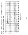
- the Al 2 O 3 layer is optically transparent in the visible.
- the coated substrate may be flexed without loss of the coating.
- One of the Al 2 O 3 barriers is coated with indium-tin oxide transparent conductor by rf magnetron sputtering from a 10% (by weight) Sn-doped indium oxide target.
- the ITO film thickness is 150 nm.
- the LEP is spin coated on the ITO electrode, after which a cathode of 5 nm Ca with about 1 ⁇ m of Al are thermally evaporated from Ca and Al metal sources, respectively.
- This LEP device is then coated with a 50 nm-thick, top barrier layer film of Al 2 O 3 , deposited by atomic layer deposition, again using trimethylaluminum as the precursor for aluminum and ozone (O 3 ) as the oxidant.
- the resulting structure is now impervious to atmospheric gases.
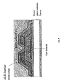
- FIG. 2 Another version of a packaging scheme is shown in Figure 2 .
- the top-coated barrier is replaced by an identical substrate barrier structure (Al 2 O 3 /PEN/Al 2 O 3 ) without an ITO electrode as described in the Example 1 above.
- This capping barrier structure is sealed to the substrate barrier using a layer of epoxy.
- Figure 3 illustrates a protection strategy with ALD barrier coatings for an organic transistor.
- the transistor shown is a bottom gate structure with the organic semiconductor as the final or top layer. Because most organic semiconductors are air sensitive and prolonged exposure degrades their properties, protection strategies are necessary.
- the package is comprised of a barrier-substrate on which the transistor is deposited and then sealed to an identical capping barrier structure.
- the substrate is comprised of a polyester film, polyethylene naphthalate (PEN), 0.004 inch (101.6 ⁇ m) thick.
- PEN polyethylene naphthalate
- Each side of the PEN film is coated with a 50 nm thick film of Al 2 O 3 , which is deposited by atomic layer deposition, using trimethylaluminum as the precursor for aluminum and ozone (O 3 ) as the oxidant.
- the substrate temperature during deposition is 150°C.
- the PEN substrate is placed in a vacuum chamber equipped with a mechanical pump. The chamber is evacuated.
- the trimethylaluminum precursor is admitted to the chamber at a pressure of 500 millitorr (66.7 Pa) for approximately 2 seconds.
- the chamber is then purged with argon for approximately 2 seconds.
- the oxidant, ozone is then admitted to the chamber at approximately 500 millitorr (66.7 Pa) for approximately 2 seconds. Finally, the oxidant is purged with argon for approximately 2 seconds. This deposition process is repeated approximately 50 times to obtain a coating approximately 100 nanometers in thickness.
- a gate electrode of 100 nm thick Pd metal is ion-beam sputtered through a shadow mask on to the barrier film of Al 2 O 3 .
- a gate dielectric of 250 nm Si 3 N 4 is then deposited by plasma-enhanced chemical vapor deposition, also through a mask to allow contact to the metal gate. This is followed by patterning of 100 nm-thick Pd source and drain electrodes, ion beam sputtered on the gate dielectric.
- the top organic semiconductor e.g. pentacene, is thermally evaporated through a shadow mask that allows contact to source-drain electrodes.
- the entire transistor is capped with an Al 2 O 3 /PEN/Al 2 O 3 barrier-structure, sealed to substrate barrier with an epoxy sealant.
- the capping barrier of Example 3 can be replaced by a single layer of 50 nm-thick Al 2 O 3 , deposited by atomic layer deposition, using trimethylaluminum as the precursor for aluminum and ozone (O 3 ) as the oxidant.
- Both packaging structures for the organic transistor device are impervious to atmospheric gases.
- the plastic substrate with barrier coatings can also be replaced by an impermeable glass substrate.
- the barrier capping layer is comprised of an initial adhesion layer of silicon nitride deposited by plasma-enhanced chemical vapor deposition at room temperature, followed by a 50 nm-thick Al2O3 barrier, deposited by atomic layer deposition, as described in Example 3.
- PEN polyethylene terephthalate
- the coated PEN substrate was flexed at least once to a radius of at least 1.5 inches (3.81 cm) to remove the coated Al 2 O 3 -coated PEN substrate from the rigid silicon carrier wafer, to which it was attached with Kapton® tape during ALD deposition.
- the oxygen transport rate with 50% relative humidity was measured with a commercial instrument (MOCON Ox-Tran 2/20) through the film with Al 2 O 3 deposited by ALD.
Landscapes
- Chemical & Material Sciences (AREA)
- Organic Chemistry (AREA)
- General Chemical & Material Sciences (AREA)
- Chemical Kinetics & Catalysis (AREA)
- Engineering & Computer Science (AREA)
- Materials Engineering (AREA)
- Mechanical Engineering (AREA)
- Metallurgy (AREA)
- Optics & Photonics (AREA)
- Physics & Mathematics (AREA)
- Inorganic Chemistry (AREA)
- Electroluminescent Light Sources (AREA)
- Chemical Vapour Deposition (AREA)
- Laminated Bodies (AREA)
- Formation Of Insulating Films (AREA)
- Physical Vapour Deposition (AREA)
- Thin Film Transistor (AREA)
- Wrappers (AREA)
Claims (14)
- Article comprenant :a) un substrat polymère souple ayant une face supérieure et une face inférieure, etb) une barrière à la perméation des gaz ayant une épaisseur de 2 nanomètres à 100 nanomètres déposée sur l'une ou l'autre desdites faces supérieure et inférieure dudit substrat ou sur les deux par dépôt de couches atomiques.
- Article comprenant :a) un substrat polymère souple ayant une face supérieure et une face inférieure,b) une couche d'adhésion revêtue, etc) une barrière à la perméation des gaz ayant une épaisseur de 2 nanomètres à 100 nanomètres déposée sur l'une ou l'autre desdites faces supérieure et inférieure dudit substrat ou sur les deux par dépôt de couches atomiques.
- Article comprenant :a) un substrat polymère souple,b) un semi-conducteur organique, etc) une barrière à la perméation des gaz ayant une épaisseur de 2 nanomètres à 100 nanomètres déposée par dépôt de couches atomiques.
- Article comprenant :a) un substrat polymère souple,b) un polymère à cristaux liquides, etc) une barrière à la perméation des gaz ayant une épaisseur de 2 nanomètres à 100 nanomètres déposée par dépôt de couches atomiques.
- Article selon l'une quelconque des revendications 1 à 4, dans lequel chaque barrière à la perméation des gaz a une épaisseur de 2 à 50 nanomètres.
- Article selon l'une quelconque des revendications 1 à 5, dans lequel le substrat subit une dégradation chimique et/ou des changements de dimensions au-dessus de 250°C.
- Article selon l'une quelconque des revendications 1 à 6, où l'article est un récipient enfermé.
- Article selon l'une quelconque des revendications 1 à 6, où l'article est un dispositif électrique ou électronique.
- Article selon l'une quelconque des revendications 1 à 6, où l'article est un dispositif polymère d'émission de lumière.
- Article selon l'une quelconque des revendications 1 à 6, où l'article est une diode organique luminescente, un transistor, une cellule photovoltaïque organique ou un dispositif d'affichage à cristaux liquides.
- Article selon l'une quelconque des revendications 1 à 6, où l'article est un circuit comprenant un dispositif polymère luminescent.
- Article selon l'une quelconque des revendications 1 à 6, où l'article est un circuit comprenant un transistor.
- Second article comprenant une pluralité de couches, chaque couche comprenant un article, tel que décrit selon l'une quelconque des revendications 1 à 6, dans lequel les articles se trouvent en contact l'un avec l'autre.
- Second article selon la revendication 14, dans lequel les articles se trouvent en contact l'un avec l'autre par des moyens de stratification.
Applications Claiming Priority (2)
| Application Number | Priority Date | Filing Date | Title |
|---|---|---|---|
| US47102003P | 2003-05-16 | 2003-05-16 | |
| PCT/US2004/015270 WO2004105149A1 (fr) | 2003-05-16 | 2004-05-14 | Films barrieres pour substrats en plastique fabriques par depot de couches atomiques |
Publications (2)
| Publication Number | Publication Date |
|---|---|
| EP1629543A1 EP1629543A1 (fr) | 2006-03-01 |
| EP1629543B1 true EP1629543B1 (fr) | 2013-08-07 |
Family
ID=33476779
Family Applications (1)
| Application Number | Title | Priority Date | Filing Date |
|---|---|---|---|
| EP04785558.0A Revoked EP1629543B1 (fr) | 2003-05-16 | 2004-05-14 | Films barrieres pour substrats polymers flexibles fabriques par depot de couches atomiques |
Country Status (6)
| Country | Link |
|---|---|
| US (3) | US20070275181A1 (fr) |
| EP (1) | EP1629543B1 (fr) |
| JP (3) | JP2007516347A (fr) |
| KR (3) | KR20060006840A (fr) |
| CN (2) | CN103215569A (fr) |
| WO (1) | WO2004105149A1 (fr) |
Cited By (3)
| Publication number | Priority date | Publication date | Assignee | Title |
|---|---|---|---|---|
| EP3476594A1 (fr) | 2017-10-24 | 2019-05-01 | Renolit SE | Structure stratifiée pour emballage barrière biocompatible |
| EP3476593A1 (fr) | 2017-10-24 | 2019-05-01 | Renolit SE | Structure de stratifié? pour emballage barrière |
| WO2023025634A1 (fr) | 2021-08-23 | 2023-03-02 | Saint-Gobain Glass France | Entretoise ayant une barrière contre l'humidité |
Families Citing this family (113)
| Publication number | Priority date | Publication date | Assignee | Title |
|---|---|---|---|---|
| KR100544145B1 (ko) * | 2004-05-24 | 2006-01-23 | 삼성에스디아이 주식회사 | 박막 트랜지스터 및 이를 구비한 평판표시장치 |
| WO2006014591A2 (fr) * | 2004-07-08 | 2006-02-09 | Itn Energy Systems, Inc. | Dispositif de protection contre la permeation pour dispositifs electroniques flexibles |
| DE102004061464B4 (de) * | 2004-12-17 | 2008-12-11 | Schott Ag | Substrat mit feinlaminarer Barriereschutzschicht und Verfahren zu dessen Herstellung |
| KR101122231B1 (ko) * | 2004-12-17 | 2012-03-19 | 삼성전자주식회사 | 유기 반도체를 이용한 박막 트랜지스터 표시판 및 그 제조방법 |
| US7722929B2 (en) | 2005-08-18 | 2010-05-25 | Corning Incorporated | Sealing technique for decreasing the time it takes to hermetically seal a device and the resulting hermetically sealed device |
| US20070040501A1 (en) | 2005-08-18 | 2007-02-22 | Aitken Bruce G | Method for inhibiting oxygen and moisture degradation of a device and the resulting device |
| US7829147B2 (en) | 2005-08-18 | 2010-11-09 | Corning Incorporated | Hermetically sealing a device without a heat treating step and the resulting hermetically sealed device |
| US7508130B2 (en) | 2005-11-18 | 2009-03-24 | Eastman Kodak Company | OLED device having improved light output |
| KR101449076B1 (ko) * | 2006-11-13 | 2015-02-23 | 더 리젠츠 오브 더 유니버시티 오브 콜로라도, 어 바디 코포레이트 | 유기 또는 유기-무기 폴리머 제조를 위한 분자층 증착 공정 |
| US8115326B2 (en) | 2006-11-30 | 2012-02-14 | Corning Incorporated | Flexible substrates having a thin-film barrier |
| US7781031B2 (en) | 2006-12-06 | 2010-08-24 | General Electric Company | Barrier layer, composite article comprising the same, electroactive device, and method |
| US7646144B2 (en) | 2006-12-27 | 2010-01-12 | Eastman Kodak Company | OLED with protective bi-layer electrode |
| US7750558B2 (en) | 2006-12-27 | 2010-07-06 | Global Oled Technology Llc | OLED with protective electrode |
| US8174187B2 (en) | 2007-01-15 | 2012-05-08 | Global Oled Technology Llc | Light-emitting device having improved light output |
| US20090159119A1 (en) * | 2007-03-28 | 2009-06-25 | Basol Bulent M | Technique and apparatus for manufacturing flexible and moisture resistive photovoltaic modules |
| US7795613B2 (en) * | 2007-04-17 | 2010-09-14 | Toppan Printing Co., Ltd. | Structure with transistor |
| DE102007019994A1 (de) * | 2007-04-27 | 2008-10-30 | Fraunhofer-Gesellschaft zur Förderung der angewandten Forschung e.V. | Transparente Barrierefolie und Verfahren zum Herstellen derselben |
| US7560747B2 (en) | 2007-05-01 | 2009-07-14 | Eastman Kodak Company | Light-emitting device having improved light output |
| US20090081356A1 (en) | 2007-09-26 | 2009-03-26 | Fedorovskaya Elena A | Process for forming thin film encapsulation layers |
| US20090081360A1 (en) | 2007-09-26 | 2009-03-26 | Fedorovskaya Elena A | Oled display encapsulation with the optical property |
| US8080280B1 (en) | 2007-10-16 | 2011-12-20 | Sandia Corporation | Nanostructure templating using low temperature atomic layer deposition |
| FI120832B (fi) * | 2007-12-03 | 2010-03-31 | Beneq Oy | Menetelmä ohuen lasin lujuuden kasvattamiseksi |
| US7993733B2 (en) | 2008-02-20 | 2011-08-09 | Applied Materials, Inc. | Index modified coating on polymer substrate |
| US20090238993A1 (en) * | 2008-03-19 | 2009-09-24 | Applied Materials, Inc. | Surface preheating treatment of plastics substrate |
| GB0807037D0 (en) * | 2008-04-17 | 2008-05-21 | Dupont Teijin Films Us Ltd | Coated polymeric films |
| US8057649B2 (en) | 2008-05-06 | 2011-11-15 | Applied Materials, Inc. | Microwave rotatable sputtering deposition |
| US8349156B2 (en) | 2008-05-14 | 2013-01-08 | Applied Materials, Inc. | Microwave-assisted rotatable PVD |
| US8242487B2 (en) | 2008-05-16 | 2012-08-14 | E I Du Pont De Nemours And Company | Anode for an organic electronic device |
| US7976908B2 (en) * | 2008-05-16 | 2011-07-12 | General Electric Company | High throughput processes and systems for barrier film deposition and/or encapsulation of optoelectronic devices |
| FR2933538B1 (fr) * | 2008-07-07 | 2012-09-21 | Commissariat Energie Atomique | Dispositif electroluminescent d'affichage, d'eclairage ou de signalisation, et son procede de fabrication |
| DE102008054052A1 (de) | 2008-10-30 | 2010-05-06 | Osram Opto Semiconductors Gmbh | Organisches, strahlungsemittierendes Bauelement und Verfahren zur Herstellung eines solchen |
| JP2012510706A (ja) * | 2008-12-01 | 2012-05-10 | イー・アイ・デュポン・ドウ・ヌムール・アンド・カンパニー | 有機電子デバイス用のアノード |
| CN102239278A (zh) * | 2008-12-05 | 2011-11-09 | 莲花应用技术有限责任公司 | 具有改进的阻隔层性能的薄膜的高速沉积 |
| JP2010140980A (ja) * | 2008-12-10 | 2010-06-24 | Sony Corp | 機能性有機物素子及び機能性有機物装置 |
| CN102257621B (zh) * | 2008-12-19 | 2013-08-21 | 株式会社半导体能源研究所 | 晶体管的制造方法 |
| US8461758B2 (en) * | 2008-12-19 | 2013-06-11 | E I Du Pont De Nemours And Company | Buffer bilayers for electronic devices |
| DE102009024411A1 (de) * | 2009-03-24 | 2010-09-30 | Osram Opto Semiconductors Gmbh | Dünnschichtverkapselung für ein optoelektronisches Bauelement, Verfahren zu dessen Herstellung und optoelektronisches Bauelement |
| FI123170B (fi) * | 2009-05-26 | 2012-11-30 | Beneq Oy | Järjestely substraatin käsittelemiseksi sekä asennusalusta substraattia varten |
| CN102484160A (zh) * | 2009-08-24 | 2012-05-30 | 纳幕尔杜邦公司 | 用于薄膜光伏电池的阻挡膜 |
| FI20095947A0 (fi) * | 2009-09-14 | 2009-09-14 | Beneq Oy | Monikerrospinnoite, menetelmä monikerrospinnoitteen valmistamiseksi, ja sen käyttötapoja |
| JP5621258B2 (ja) * | 2009-12-28 | 2014-11-12 | ソニー株式会社 | 成膜装置および成膜方法 |
| US8637123B2 (en) | 2009-12-29 | 2014-01-28 | Lotus Applied Technology, Llc | Oxygen radical generation for radical-enhanced thin film deposition |
| FI122616B (fi) * | 2010-02-02 | 2012-04-30 | Beneq Oy | Vahvistettu rakennemoduuli ja sen valmistusmenetelmä |
| US8512809B2 (en) | 2010-03-31 | 2013-08-20 | General Electric Company | Method of processing multilayer film |
| JP5912228B2 (ja) * | 2010-05-17 | 2016-04-27 | 凸版印刷株式会社 | ガスバリア性積層体の製造方法 |
| DE102010040839B4 (de) * | 2010-09-15 | 2013-10-17 | Osram Opto Semiconductors Gmbh | Verfahren zum Herstellen eines elektronsichen Bauelements und elektronisches Bauelement |
| JP2012096432A (ja) * | 2010-11-01 | 2012-05-24 | Sony Corp | バリアフィルム及びその製造方法 |
| CN102468307A (zh) * | 2010-11-15 | 2012-05-23 | 联建(中国)科技有限公司 | 基板模组、显示面板以及触控面板 |
| JP2012182303A (ja) * | 2011-03-01 | 2012-09-20 | Toppan Printing Co Ltd | 太陽電池バックシート |
| DE102011079101A1 (de) * | 2011-07-13 | 2013-01-17 | Osram Opto Semiconductors Gmbh | Organisches optoelektronisches bauteil und verfahren zu dessen herstellung |
| TWI590951B (zh) | 2011-07-28 | 2017-07-11 | 凸版印刷股份有限公司 | 積層體、阻氣薄膜、積層體之製造方法及積層體製造裝置 |
| JP6251937B2 (ja) | 2011-07-28 | 2017-12-27 | 凸版印刷株式会社 | 積層体、ガスバリアフィルム、及びこれらの製造方法 |
| TW201322382A (zh) * | 2011-11-17 | 2013-06-01 | Wintek Corp | 電致發光顯示裝置 |
| US20150099126A1 (en) | 2012-04-25 | 2015-04-09 | Konica Minolta, Inc. | Gas barrier film, substrate for electronic device and electronic device |
| US20130333835A1 (en) * | 2012-06-14 | 2013-12-19 | E I Du Pont De Nemours And Company | Process for manufacturing gas permeation barrier material and structure |
| US10862073B2 (en) * | 2012-09-25 | 2020-12-08 | The Trustees Of Princeton University | Barrier film for electronic devices and substrates |
| TWI592310B (zh) | 2012-10-18 | 2017-07-21 | 凸版印刷股份有限公司 | 積層體、阻氣薄膜及其製造方法 |
| US10096533B2 (en) * | 2014-11-17 | 2018-10-09 | Sage Electrochromics, Inc. | Multiple barrier layer encapsulation stack |
| DE102012220586A1 (de) * | 2012-11-12 | 2014-05-15 | Osram Opto Semiconductors Gmbh | Element zur Stabilisierung eines optoelektronischen Bauelements, Verfahren zur Herstellung eines Elements und optoelektronisches Bauelement |
| JP2016502465A (ja) * | 2012-11-29 | 2016-01-28 | エルジー・ケム・リミテッド | バリア層の損傷を低減させるコーティング方法 |
| KR101583119B1 (ko) * | 2012-11-29 | 2016-01-07 | 주식회사 엘지화학 | 가스차단성 필름 |
| DE102013100818B4 (de) * | 2013-01-28 | 2023-07-27 | OSRAM Opto Semiconductors Gesellschaft mit beschränkter Haftung | Optoelektronischer Halbleiterchip und Verfahren zur Herstellung eines optoelektronischen Halbleiterchips |
| DE112014000637T5 (de) * | 2013-01-31 | 2015-11-05 | E.I. Du Pont De Nemours And Company | Gasdurchgangs-Sperrschichtmaterial und damit konstruierte elektronische Geräte |
| KR101701257B1 (ko) * | 2013-03-14 | 2017-02-01 | 어플라이드 머티어리얼스, 인코포레이티드 | 박막 캡슐화 ― oled 어플리케이션을 위한 얇은 초고 배리어 층 |
| WO2014156888A1 (fr) * | 2013-03-27 | 2014-10-02 | 凸版印刷株式会社 | Stratifié et film de barrière contre les gaz |
| EP2979857B1 (fr) | 2013-03-27 | 2024-03-20 | Toppan Printing Co., Ltd. | Corps stratifié, film de barrière et procédé de fabrication de ceux-ci |
| JP6003778B2 (ja) | 2013-04-03 | 2016-10-05 | 株式会社デンソー | 熱交換器の製造方法 |
| US20140319488A1 (en) * | 2013-04-25 | 2014-10-30 | Veeco Ald Inc. | Thin film formation for device sensitive to environment |
| JP2014214366A (ja) * | 2013-04-26 | 2014-11-17 | コニカミノルタ株式会社 | プラズマcvd成膜用マスク、プラズマcvd成膜方法、及び有機エレクトロルミネッセンス素子 |
| JP6020339B2 (ja) * | 2013-04-26 | 2016-11-02 | コニカミノルタ株式会社 | プラズマcvd成膜用マスク、及びプラズマcvd成膜方法 |
| KR102104608B1 (ko) * | 2013-05-16 | 2020-04-27 | 삼성디스플레이 주식회사 | 유기 발광 표시 장치, 이를 포함하는 전자 기기, 및 유기 발광 표시 장치의 제조 방법 |
| FR3006236B1 (fr) * | 2013-06-03 | 2016-07-29 | Commissariat Energie Atomique | Procede de collage metallique direct |
| KR101928598B1 (ko) * | 2013-09-30 | 2018-12-12 | 주식회사 엘지화학 | 폴리이미드 필름 및 그 제조방법 |
| US9761832B2 (en) | 2013-09-30 | 2017-09-12 | Lg Display Co., Ltd. | Substrate for organic electronic device |
| JP2015115185A (ja) * | 2013-12-11 | 2015-06-22 | 東京エレクトロン株式会社 | 有機elモジュールおよびその製造方法 |
| CN103955091A (zh) * | 2014-05-22 | 2014-07-30 | 张家港康得新光电材料有限公司 | 基于pdlc器件的光学复合膜及其制备方法 |
| DE102014010241A1 (de) * | 2014-05-30 | 2015-12-03 | Schott Ag | Körper, bevorzugt mit einer Oberfläche umfassend bevorzugt einen Glaskörper mit einer Glasoberfläche und Verfahren zur Herstellung desselben |
| KR102278917B1 (ko) | 2014-07-24 | 2021-07-20 | 오스람 오엘이디 게엠베하 | 배리어층을 형성하는 방법 및 상기 배리어층을 포함하는 지지체 |
| JP6812793B2 (ja) | 2014-07-29 | 2021-01-13 | 凸版印刷株式会社 | 積層体及びその製造方法、並びにガスバリアフィルム及びその製造方法 |
| CN104300091B (zh) * | 2014-09-17 | 2017-02-15 | 合肥京东方光电科技有限公司 | Oled器件封装结构及其制作方法 |
| JP2017533995A (ja) * | 2014-10-17 | 2017-11-16 | ロータス アプライド テクノロジー エルエルシーLotus Applied Technology, Llc | 混合酸化バリア膜の高速堆積 |
| WO2016061524A1 (fr) * | 2014-10-17 | 2016-04-21 | Dickey Eric R | Dépôt de films barrières d'oxyde mixte de haute qualité |
| CN111477657B (zh) * | 2014-10-28 | 2024-03-05 | 株式会社半导体能源研究所 | 功能面板、功能面板的制造方法、模块、数据处理装置 |
| CN104465636A (zh) * | 2014-11-12 | 2015-03-25 | 谢颃星 | 一种新型半导体封装体 |
| JP5795427B1 (ja) * | 2014-12-26 | 2015-10-14 | 竹本容器株式会社 | 被膜付き樹脂容器の製造方法及び樹脂容器被覆装置 |
| US9766763B2 (en) | 2014-12-26 | 2017-09-19 | Semiconductor Energy Laboratory Co., Ltd. | Functional panel, light-emitting panel, display panel, and sensor panel |
| JP6011652B2 (ja) * | 2015-02-02 | 2016-10-19 | 凸版印刷株式会社 | ガスバリア性積層体およびこの製造方法 |
| JP6554810B2 (ja) * | 2015-02-16 | 2019-08-07 | 凸版印刷株式会社 | 積層体及びその製造方法、並びにガスバリアフィルム |
| JP6524702B2 (ja) | 2015-02-26 | 2019-06-05 | 凸版印刷株式会社 | ガスバリア性フィルムの製造方法及びガスバリア性フィルム |
| JP6536105B2 (ja) | 2015-03-17 | 2019-07-03 | 凸版印刷株式会社 | 積層体及びその製造方法、並びにガスバリアフィルム及びその製造方法 |
| WO2016167348A1 (fr) * | 2015-04-16 | 2016-10-20 | 凸版印刷株式会社 | Stratifié et film formant barrière aux gaz |
| JP6657588B2 (ja) | 2015-04-17 | 2020-03-04 | 凸版印刷株式会社 | 積層体及びその製造方法 |
| JP6259023B2 (ja) | 2015-07-20 | 2018-01-10 | ウルトラテック インク | 電極系デバイス用のald処理のためのマスキング方法 |
| CN105449123B (zh) * | 2015-11-18 | 2018-03-06 | 上海大学 | 水氧阻隔层的制备方法 |
| EP3398769B1 (fr) | 2015-12-28 | 2024-05-22 | Toppan Printing Co., Ltd. | Stratifié et son procédé de fabrication, film barrière contre les gaz et son procédé de fabrication, et élément électroluminescent organique |
| WO2017213242A1 (fr) | 2016-06-08 | 2017-12-14 | 凸版印刷株式会社 | Corps d'affichage |
| US10472150B2 (en) * | 2016-07-12 | 2019-11-12 | R.J. Reynolds Tobacco Products | Package wrapping including PLA film with moisture barrier by atomic layer deposition |
| KR102577001B1 (ko) | 2016-08-11 | 2023-09-12 | 삼성디스플레이 주식회사 | 플렉서블 기판, 플렉서블 기판의 제조방법, 및 플렉서블 기판을 포함하는 디스플레이 장치 |
| CN106947957A (zh) * | 2017-03-01 | 2017-07-14 | 秦皇岛博硕光电设备股份有限公司 | 食品/药品容器的加工方法、食品/药品容器用材料及食品/药品容器 |
| CN107068904A (zh) * | 2017-04-18 | 2017-08-18 | 京东方科技集团股份有限公司 | 无机封装薄膜、oled封装薄膜的制作方法及相应装置 |
| FR3066324B1 (fr) * | 2017-05-11 | 2021-09-10 | Isorg | Dispositif electronique a tenue au vieillissement amelioree |
| CN111971168B (zh) | 2018-02-02 | 2023-09-05 | 凸版印刷株式会社 | 阻气膜及其制造方法 |
| EP3843128B1 (fr) | 2018-08-24 | 2024-06-19 | FUJIFILM Corporation | Procédé de fabrication d'un transistor à couches minces organiques |
| EP3914750A4 (fr) * | 2019-01-25 | 2023-02-15 | Applied Materials, Inc. | Procédé de formation de revêtements barrières contre l'humidité et l'oxygène |
| FR3098997B1 (fr) * | 2019-07-18 | 2021-11-26 | Tecmoled | Dispositif d’émission de lumière |
| CN111172511A (zh) * | 2020-01-17 | 2020-05-19 | 胜科纳米(苏州)有限公司 | 一种在有机材料表面制备金属膜层的方法 |
| KR102270084B1 (ko) * | 2020-04-20 | 2021-06-29 | 삼성디스플레이 주식회사 | 유기 발광 표시 장치, 이를 포함하는 전자 기기, 및 유기 발광 표시 장치의 제조 방법 |
| KR102184678B1 (ko) * | 2020-04-20 | 2020-12-01 | 삼성디스플레이 주식회사 | 유기 발광 표시 장치, 이를 포함하는 전자 기기, 및 유기 발광 표시 장치의 제조 방법 |
| CN112850639A (zh) * | 2021-01-26 | 2021-05-28 | 嘉庚创新实验室 | 一种微纳器件聚合物、制备方法及应用 |
| US12347652B2 (en) | 2021-05-24 | 2025-07-01 | Applied Materials, Inc. | Method for forming plasma coating |
| WO2022249112A1 (fr) * | 2021-05-25 | 2022-12-01 | Metacontinental, Inc. | Cellule photovoltaïque à emmisivité thermique accrue |
| CN115613004A (zh) * | 2021-07-12 | 2023-01-17 | 北京印刷学院 | 内壁镀膜的塑料管及制备方法 |
| US12091239B2 (en) * | 2021-11-11 | 2024-09-17 | Advanced Composite Structures, Llc | Formed structural panel with open core |
Family Cites Families (59)
| Publication number | Priority date | Publication date | Assignee | Title |
|---|---|---|---|---|
| JPH06222388A (ja) * | 1993-01-28 | 1994-08-12 | Fujitsu Ltd | 薄膜トランジスタマトリックスの製造方法 |
| US5641984A (en) | 1994-08-19 | 1997-06-24 | General Electric Company | Hermetically sealed radiation imager |
| JP2776268B2 (ja) | 1994-10-07 | 1998-07-16 | 王子製紙株式会社 | メタライズドコンデンサ用亜鉛蒸着基材及びその製造方法 |
| DE4438359C2 (de) * | 1994-10-27 | 2001-10-04 | Schott Glas | Behälter aus Kunststoff mit einer Sperrbeschichtung |
| JP3962436B2 (ja) * | 1995-02-14 | 2007-08-22 | 出光興産株式会社 | 多色発光装置 |
| WO1996025020A1 (fr) | 1995-02-06 | 1996-08-15 | Idemitsu Kosan Co., Ltd. | Dispositif emetteur de lumiere en plusieurs couleurs et procede de production de ce dispositif |
| JPH11511080A (ja) | 1995-08-21 | 1999-09-28 | イー・アイ・デユポン・ドウ・ヌムール・アンド・カンパニー | 水分のない印刷板 |
| FI954922A7 (fi) | 1995-10-16 | 1997-04-17 | Picopak Oy | Valmistusmenetelmä sekä kontaktinystyrakenne puolijohdepalojen tiheitä pintaliitoksia varten |
| US5686360A (en) * | 1995-11-30 | 1997-11-11 | Motorola | Passivation of organic devices |
| US5693956A (en) * | 1996-07-29 | 1997-12-02 | Motorola | Inverted oleds on hard plastic substrate |
| JP3290375B2 (ja) * | 1997-05-12 | 2002-06-10 | 松下電器産業株式会社 | 有機電界発光素子 |
| EP1021255A1 (fr) * | 1997-07-11 | 2000-07-26 | Fed Corporation | Structure de fermeture hermetique pour dispositifs photo-emetteurs organiques |
| KR100492983B1 (ko) | 1997-07-23 | 2005-09-02 | 삼성전자주식회사 | 화학기상증착장치및그장치를이용하는금속배선형성방법 |
| KR100635429B1 (ko) * | 1998-08-03 | 2006-10-18 | 듀폰 디스플레이즈, 인크. | 무기 재료를 사용한 중합체-기재 고체 장치의 캡슐화 |
| US6268695B1 (en) * | 1998-12-16 | 2001-07-31 | Battelle Memorial Institute | Environmental barrier material for organic light emitting device and method of making |
| IL145317A0 (en) * | 1999-04-28 | 2002-06-30 | Du Pont | Flexible organic electronic device with improved resistance to oxygen and moisture degradation |
| US6203613B1 (en) | 1999-10-19 | 2001-03-20 | International Business Machines Corporation | Atomic layer deposition with nitrate containing precursors |
| US6548912B1 (en) * | 1999-10-25 | 2003-04-15 | Battelle Memorial Institute | Semicoductor passivation using barrier coatings |
| US6623861B2 (en) * | 2001-04-16 | 2003-09-23 | Battelle Memorial Institute | Multilayer plastic substrates |
| US6633121B2 (en) * | 2000-01-31 | 2003-10-14 | Idemitsu Kosan Co., Ltd. | Organic electroluminescence display device and method of manufacturing same |
| US6368899B1 (en) | 2000-03-08 | 2002-04-09 | Maxwell Electronic Components Group, Inc. | Electronic device packaging |
| JP4556282B2 (ja) * | 2000-03-31 | 2010-10-06 | 株式会社デンソー | 有機el素子およびその製造方法 |
| US20010052752A1 (en) * | 2000-04-25 | 2001-12-20 | Ghosh Amalkumar P. | Thin film encapsulation of organic light emitting diode devices |
| US7579203B2 (en) | 2000-04-25 | 2009-08-25 | Semiconductor Energy Laboratory Co., Ltd. | Light emitting device |
| JP4827313B2 (ja) * | 2000-04-25 | 2011-11-30 | 株式会社半導体エネルギー研究所 | 発光装置の作製方法 |
| US20020086307A1 (en) | 2000-07-06 | 2002-07-04 | Murtaza Amin | Combination of microporous membrane and solid support for micro-analytical diagnostic applications |
| JP2002018994A (ja) * | 2000-07-12 | 2002-01-22 | Sony Corp | ガスバリア材及び有機エレクトロルミネッセンス素子 |
| JP2002100469A (ja) * | 2000-09-25 | 2002-04-05 | Pioneer Electronic Corp | 有機エレクトロルミネッセンス表示パネル |
| US6664186B1 (en) | 2000-09-29 | 2003-12-16 | International Business Machines Corporation | Method of film deposition, and fabrication of structures |
| JP2002134272A (ja) * | 2000-10-25 | 2002-05-10 | Ricoh Co Ltd | エレクトロルミネセンス素子及びその作製方法 |
| JP4374765B2 (ja) * | 2000-11-09 | 2009-12-02 | 株式会社デンソー | 有機el素子の製造方法 |
| WO2002065558A2 (fr) * | 2001-02-05 | 2002-08-22 | Dow Global Technologies Inc. | Diodes luminescentes organiques sur des substrats plastiques |
| WO2002071506A1 (fr) * | 2001-02-15 | 2002-09-12 | Emagin Corporation | Encapsulation en couche mince de dispositifs a diodes organiques electroluminescentes (oled) |
| JP2002273811A (ja) * | 2001-03-16 | 2002-09-25 | Sumitomo Bakelite Co Ltd | 光学用高分子シート |
| US6624568B2 (en) * | 2001-03-28 | 2003-09-23 | Universal Display Corporation | Multilayer barrier region containing moisture- and oxygen-absorbing material for optoelectronic devices |
| JP2003086356A (ja) * | 2001-09-06 | 2003-03-20 | Semiconductor Energy Lab Co Ltd | 発光装置及び電子機器 |
| US7211828B2 (en) * | 2001-06-20 | 2007-05-01 | Semiconductor Energy Laboratory Co., Ltd. | Light emitting device and electronic apparatus |
| US20030008243A1 (en) | 2001-07-09 | 2003-01-09 | Micron Technology, Inc. | Copper electroless deposition technology for ULSI metalization |
| CA2452656C (fr) * | 2001-07-18 | 2010-04-13 | The Regents Of The University Of Colorado | Une methode pour deposer une couche mince inorganique sur un polymere organique |
| JP2003051386A (ja) * | 2001-08-06 | 2003-02-21 | Toppan Printing Co Ltd | 有機エレクトロルミネッセンス素子 |
| TW490868B (en) * | 2001-08-10 | 2002-06-11 | Ritdisplay Corp | Method for forming a waterproof layer of organic light emitting device |
| US6794220B2 (en) * | 2001-09-05 | 2004-09-21 | Konica Corporation | Organic thin-film semiconductor element and manufacturing method for the same |
| US6605549B2 (en) | 2001-09-29 | 2003-08-12 | Intel Corporation | Method for improving nucleation and adhesion of CVD and ALD films deposited onto low-dielectric-constant dielectrics |
| JP2003125315A (ja) * | 2001-10-19 | 2003-04-25 | Sony Corp | 画像表示装置 |
| US6926572B2 (en) | 2002-01-25 | 2005-08-09 | Electronics And Telecommunications Research Institute | Flat panel display device and method of forming passivation film in the flat panel display device |
| US6897474B2 (en) * | 2002-04-12 | 2005-05-24 | Universal Display Corporation | Protected organic electronic devices and methods for making the same |
| US6949389B2 (en) * | 2002-05-02 | 2005-09-27 | Osram Opto Semiconductors Gmbh | Encapsulation for organic light emitting diodes devices |
| JP4048830B2 (ja) * | 2002-05-16 | 2008-02-20 | 株式会社デンソー | 有機電子デバイス素子 |
| JP2004165634A (ja) | 2002-08-15 | 2004-06-10 | Interuniv Micro Electronica Centrum Vzw | Ald表面処理のためのプラズマ処理 |
| US20040229051A1 (en) * | 2003-05-15 | 2004-11-18 | General Electric Company | Multilayer coating package on flexible substrates for electro-optical devices |
| US7015640B2 (en) * | 2002-09-11 | 2006-03-21 | General Electric Company | Diffusion barrier coatings having graded compositions and devices incorporating the same |
| JP2004288456A (ja) * | 2003-03-20 | 2004-10-14 | Denso Corp | 有機elパネル |
| US7018713B2 (en) * | 2003-04-02 | 2006-03-28 | 3M Innovative Properties Company | Flexible high-temperature ultrabarrier |
| US6888172B2 (en) * | 2003-04-11 | 2005-05-03 | Eastman Kodak Company | Apparatus and method for encapsulating an OLED formed on a flexible substrate |
| US7352053B2 (en) | 2003-10-29 | 2008-04-01 | Taiwan Semiconductor Manufacturing Company, Ltd. | Insulating layer having decreased dielectric constant and increased hardness |
| US20050172897A1 (en) | 2004-02-09 | 2005-08-11 | Frank Jansen | Barrier layer process and arrangement |
| US7115304B2 (en) | 2004-02-19 | 2006-10-03 | Nanosolar, Inc. | High throughput surface treatment on coiled flexible substrates |
| US7541626B2 (en) | 2005-03-28 | 2009-06-02 | Massachusetts Institute Of Technology | High K-gate oxide TFTs built on transparent glass or transparent flexible polymer substrate |
| JP2007090803A (ja) | 2005-09-30 | 2007-04-12 | Fujifilm Corp | ガスバリアフィルム、並びに、これを用いた画像表示素子および有機エレクトロルミネッセンス素子 |
-
2004
- 2004-05-14 KR KR1020057021773A patent/KR20060006840A/ko not_active Ceased
- 2004-05-14 JP JP2006533109A patent/JP2007516347A/ja active Pending
- 2004-05-14 US US10/846,749 patent/US20070275181A1/en not_active Abandoned
- 2004-05-14 CN CN2013101015014A patent/CN103215569A/zh active Pending
- 2004-05-14 KR KR1020137014284A patent/KR101423446B1/ko not_active Expired - Fee Related
- 2004-05-14 KR KR1020127007255A patent/KR20120061906A/ko not_active Ceased
- 2004-05-14 CN CNA2004800134392A patent/CN1791989A/zh active Pending
- 2004-05-14 WO PCT/US2004/015270 patent/WO2004105149A1/fr not_active Ceased
- 2004-05-14 EP EP04785558.0A patent/EP1629543B1/fr not_active Revoked
-
2005
- 2005-05-03 US US10/554,583 patent/US20060275926A1/en not_active Abandoned
-
2008
- 2008-03-26 US US12/055,560 patent/US8445937B2/en not_active Expired - Fee Related
-
2011
- 2011-06-20 JP JP2011136790A patent/JP2011205133A/ja active Pending
-
2012
- 2012-04-12 JP JP2012090941A patent/JP2012184509A/ja active Pending
Cited By (7)
| Publication number | Priority date | Publication date | Assignee | Title |
|---|---|---|---|---|
| EP3476594A1 (fr) | 2017-10-24 | 2019-05-01 | Renolit SE | Structure stratifiée pour emballage barrière biocompatible |
| EP3476593A1 (fr) | 2017-10-24 | 2019-05-01 | Renolit SE | Structure de stratifié? pour emballage barrière |
| WO2019081176A1 (fr) | 2017-10-24 | 2019-05-02 | Renolit Se | Structure stratifiée pour emballage barrière biocompatible |
| WO2019081175A1 (fr) | 2017-10-24 | 2019-05-02 | Renolit Se | Structure stratifiée destinée à un emballage barrière |
| US11254108B2 (en) | 2017-10-24 | 2022-02-22 | Renolit Se | Laminate structure for biocompatible barrier packaging |
| US11654660B2 (en) | 2017-10-24 | 2023-05-23 | Renolit Se | Laminate structure for barrier packaging |
| WO2023025634A1 (fr) | 2021-08-23 | 2023-03-02 | Saint-Gobain Glass France | Entretoise ayant une barrière contre l'humidité |
Also Published As
| Publication number | Publication date |
|---|---|
| US20070275181A1 (en) | 2007-11-29 |
| JP2011205133A (ja) | 2011-10-13 |
| KR101423446B1 (ko) | 2014-07-24 |
| US20060275926A1 (en) | 2006-12-07 |
| JP2012184509A (ja) | 2012-09-27 |
| KR20060006840A (ko) | 2006-01-19 |
| CN103215569A (zh) | 2013-07-24 |
| JP2007516347A (ja) | 2007-06-21 |
| US8445937B2 (en) | 2013-05-21 |
| KR20120061906A (ko) | 2012-06-13 |
| WO2004105149A1 (fr) | 2004-12-02 |
| US20080182101A1 (en) | 2008-07-31 |
| CN1791989A (zh) | 2006-06-21 |
| KR20130081313A (ko) | 2013-07-16 |
| EP1629543A1 (fr) | 2006-03-01 |
Similar Documents
| Publication | Publication Date | Title |
|---|---|---|
| US8445937B2 (en) | Barrier films for plastic substrates fabricated by atomic layer deposition | |
| US20130333835A1 (en) | Process for manufacturing gas permeation barrier material and structure | |
| US7074501B2 (en) | Coatings with low permeation of gases and vapors | |
| US20130337259A1 (en) | Gas permeation barrier material | |
| US7378133B2 (en) | Fabrication system, light-emitting device and fabricating method of organic compound-containing layer | |
| EP1842873B1 (fr) | Film stratifié faisant barriere au gaz | |
| US20090087998A1 (en) | Diffusion barrier layer and method for manufacturing a diffusion barrier layer | |
| EP2374173B1 (fr) | Procédé d'encapsulation de dispositifs sensibles à l'environnement | |
| US20160254487A1 (en) | Permeation barrier system for substrates and devices and method of making the same | |
| CN105390621A (zh) | 用于衬底和装置的薄膜渗透屏障系统和制造所述薄膜渗透屏障系统的方法 | |
| US10961622B2 (en) | Gas barrier film and method of manufacturing the same | |
| CA2505014A1 (fr) | Encapsulage hermetique d'elements electro-optiques organiques | |
| JP4506365B2 (ja) | バリアフィルムの製造方法 | |
| WO2013188613A1 (fr) | Matériau de barrière de perméation de gaz | |
| JP2008240131A (ja) | 透明ガスバリアフィルムおよびエレクトロルミネッセンス素子 | |
| JP2005212230A (ja) | 透明ガスバリアフィルムおよびエレクトロルミネッセンス素子 | |
| JP2017109438A (ja) | ガスバリア性フィルム及びこれを用いた有機el発光素子 | |
| JP2005212231A (ja) | 透明ガスバリアフィルム、その製造方法およびエレクトロルミネッセンス素子 | |
| TW201032337A (en) | Protection of optoelectronic devices and method thereof | |
| KR20150022515A (ko) | 기판 적층체, 이를 포함하는 전자 소자 및 이의 제조방법 |
Legal Events
| Date | Code | Title | Description |
|---|---|---|---|
| PUAI | Public reference made under article 153(3) epc to a published international application that has entered the european phase |
Free format text: ORIGINAL CODE: 0009012 |
|
| 17P | Request for examination filed |
Effective date: 20051019 |
|
| AK | Designated contracting states |
Kind code of ref document: A1 Designated state(s): DE FR GB |
|
| DAX | Request for extension of the european patent (deleted) | ||
| RBV | Designated contracting states (corrected) |
Designated state(s): DE FR GB |
|
| 17Q | First examination report despatched |
Effective date: 20080701 |
|
| REG | Reference to a national code |
Ref country code: DE Ref legal event code: R079 Ref document number: 602004042979 Country of ref document: DE Free format text: PREVIOUS MAIN CLASS: H01L0051100000 Ipc: H01L0051520000 |
|
| GRAP | Despatch of communication of intention to grant a patent |
Free format text: ORIGINAL CODE: EPIDOSNIGR1 |
|
| RIC1 | Information provided on ipc code assigned before grant |
Ipc: C23C 16/455 20060101ALI20121130BHEP Ipc: C23C 16/40 20060101ALI20121130BHEP Ipc: H01L 51/52 20060101AFI20121130BHEP |
|
| GRAP | Despatch of communication of intention to grant a patent |
Free format text: ORIGINAL CODE: EPIDOSNIGR1 |
|
| GRAS | Grant fee paid |
Free format text: ORIGINAL CODE: EPIDOSNIGR3 |
|
| GRAA | (expected) grant |
Free format text: ORIGINAL CODE: 0009210 |
|
| INTG | Intention to grant announced |
Effective date: 20130612 |
|
| AK | Designated contracting states |
Kind code of ref document: B1 Designated state(s): DE FR GB |
|
| REG | Reference to a national code |
Ref country code: GB Ref legal event code: FG4D |
|
| REG | Reference to a national code |
Ref country code: DE Ref legal event code: R096 Ref document number: 602004042979 Country of ref document: DE Effective date: 20131002 |
|
| PLBI | Opposition filed |
Free format text: ORIGINAL CODE: 0009260 |
|
| 26 | Opposition filed |
Opponent name: VOLLNHALS, AUREL Effective date: 20140428 |
|
| PLAX | Notice of opposition and request to file observation + time limit sent |
Free format text: ORIGINAL CODE: EPIDOSNOBS2 |
|
| REG | Reference to a national code |
Ref country code: DE Ref legal event code: R026 Ref document number: 602004042979 Country of ref document: DE Effective date: 20140428 |
|
| PLAF | Information modified related to communication of a notice of opposition and request to file observations + time limit |
Free format text: ORIGINAL CODE: EPIDOSCOBS2 |
|
| PLBB | Reply of patent proprietor to notice(s) of opposition received |
Free format text: ORIGINAL CODE: EPIDOSNOBS3 |
|
| REG | Reference to a national code |
Ref country code: FR Ref legal event code: PLFP Year of fee payment: 12 |
|
| PGFP | Annual fee paid to national office [announced via postgrant information from national office to epo] |
Ref country code: DE Payment date: 20150506 Year of fee payment: 12 Ref country code: GB Payment date: 20150513 Year of fee payment: 12 |
|
| PGFP | Annual fee paid to national office [announced via postgrant information from national office to epo] |
Ref country code: FR Payment date: 20150508 Year of fee payment: 12 |
|
| RAP2 | Party data changed (patent owner data changed or rights of a patent transferred) |
Owner name: E. I. DU PONT DE NEMOURS AND COMPANY |
|
| RDAF | Communication despatched that patent is revoked |
Free format text: ORIGINAL CODE: EPIDOSNREV1 |
|
| REG | Reference to a national code |
Ref country code: DE Ref legal event code: R103 Ref document number: 602004042979 Country of ref document: DE Ref country code: DE Ref legal event code: R064 Ref document number: 602004042979 Country of ref document: DE |
|
| RDAG | Patent revoked |
Free format text: ORIGINAL CODE: 0009271 |
|
| STAA | Information on the status of an ep patent application or granted ep patent |
Free format text: STATUS: PATENT REVOKED |
|
| 27W | Patent revoked |
Effective date: 20160303 |
|
| GBPR | Gb: patent revoked under art. 102 of the ep convention designating the uk as contracting state |
Effective date: 20160303 |