EP1630880A2 - Dispositif de mémoire (CBRAM) comportant des cellules de mémoire à base d'un matériau électrolyte solide à résistance variable et procédé pour sa fabrication - Google Patents
Dispositif de mémoire (CBRAM) comportant des cellules de mémoire à base d'un matériau électrolyte solide à résistance variable et procédé pour sa fabrication Download PDFInfo
- Publication number
- EP1630880A2 EP1630880A2 EP05107162A EP05107162A EP1630880A2 EP 1630880 A2 EP1630880 A2 EP 1630880A2 EP 05107162 A EP05107162 A EP 05107162A EP 05107162 A EP05107162 A EP 05107162A EP 1630880 A2 EP1630880 A2 EP 1630880A2
- Authority
- EP
- European Patent Office
- Prior art keywords
- layer
- resistance
- deposited
- electrolyte material
- manufacturing
- Prior art date
- Legal status (The legal status is an assumption and is not a legal conclusion. Google has not performed a legal analysis and makes no representation as to the accuracy of the status listed.)
- Withdrawn
Links
Images



Classifications
-
- H—ELECTRICITY
- H10—SEMICONDUCTOR DEVICES; ELECTRIC SOLID-STATE DEVICES NOT OTHERWISE PROVIDED FOR
- H10N—ELECTRIC SOLID-STATE DEVICES NOT OTHERWISE PROVIDED FOR
- H10N70/00—Solid-state devices having no potential barriers, and specially adapted for rectifying, amplifying, oscillating or switching
- H10N70/20—Multistable switching devices, e.g. memristors
- H10N70/24—Multistable switching devices, e.g. memristors based on migration or redistribution of ionic species, e.g. anions, vacancies
- H10N70/245—Multistable switching devices, e.g. memristors based on migration or redistribution of ionic species, e.g. anions, vacancies the species being metal cations, e.g. programmable metallization cells
-
- H—ELECTRICITY
- H10—SEMICONDUCTOR DEVICES; ELECTRIC SOLID-STATE DEVICES NOT OTHERWISE PROVIDED FOR
- H10N—ELECTRIC SOLID-STATE DEVICES NOT OTHERWISE PROVIDED FOR
- H10N70/00—Solid-state devices having no potential barriers, and specially adapted for rectifying, amplifying, oscillating or switching
- H10N70/011—Manufacture or treatment of multistable switching devices
- H10N70/061—Shaping switching materials
- H10N70/063—Shaping switching materials by etching of pre-deposited switching material layers, e.g. lithography
-
- H—ELECTRICITY
- H10—SEMICONDUCTOR DEVICES; ELECTRIC SOLID-STATE DEVICES NOT OTHERWISE PROVIDED FOR
- H10N—ELECTRIC SOLID-STATE DEVICES NOT OTHERWISE PROVIDED FOR
- H10N70/00—Solid-state devices having no potential barriers, and specially adapted for rectifying, amplifying, oscillating or switching
- H10N70/801—Constructional details of multistable switching devices
- H10N70/821—Device geometry
- H10N70/826—Device geometry adapted for essentially vertical current flow, e.g. sandwich or pillar type devices
-
- H—ELECTRICITY
- H10—SEMICONDUCTOR DEVICES; ELECTRIC SOLID-STATE DEVICES NOT OTHERWISE PROVIDED FOR
- H10N—ELECTRIC SOLID-STATE DEVICES NOT OTHERWISE PROVIDED FOR
- H10N70/00—Solid-state devices having no potential barriers, and specially adapted for rectifying, amplifying, oscillating or switching
- H10N70/801—Constructional details of multistable switching devices
- H10N70/881—Switching materials
- H10N70/882—Compounds of sulfur, selenium or tellurium, e.g. chalcogenides
- H10N70/8822—Sulfides, e.g. CuS
-
- H—ELECTRICITY
- H10—SEMICONDUCTOR DEVICES; ELECTRIC SOLID-STATE DEVICES NOT OTHERWISE PROVIDED FOR
- H10N—ELECTRIC SOLID-STATE DEVICES NOT OTHERWISE PROVIDED FOR
- H10N70/00—Solid-state devices having no potential barriers, and specially adapted for rectifying, amplifying, oscillating or switching
- H10N70/801—Constructional details of multistable switching devices
- H10N70/881—Switching materials
- H10N70/882—Compounds of sulfur, selenium or tellurium, e.g. chalcogenides
- H10N70/8825—Selenides, e.g. GeSe
-
- Y—GENERAL TAGGING OF NEW TECHNOLOGICAL DEVELOPMENTS; GENERAL TAGGING OF CROSS-SECTIONAL TECHNOLOGIES SPANNING OVER SEVERAL SECTIONS OF THE IPC; TECHNICAL SUBJECTS COVERED BY FORMER USPC CROSS-REFERENCE ART COLLECTIONS [XRACs] AND DIGESTS
- Y10—TECHNICAL SUBJECTS COVERED BY FORMER USPC
- Y10S—TECHNICAL SUBJECTS COVERED BY FORMER USPC CROSS-REFERENCE ART COLLECTIONS [XRACs] AND DIGESTS
- Y10S438/00—Semiconductor device manufacturing: process
- Y10S438/90—Bulk effect device making
Definitions
- a memory device having memory cells based on a resistance variable active solid electrolyte material and method of manufacturing the same
- the invention relates to a memory device (CBRAM) having memory cells based on a variable in its resistance active solid electrolyte material, embedded between a lower and upper electrode, by applying a suitable electric field between these electrodes between an on state with a small Resistor and an off state with the opposite high resistance switchable, and a manufacturing method for it.
- CBRAM memory device
- the functional principle uses the formation and extinguishing of a low-resistance channel in a high-resistance solid-state electrolyte material when creating suitable electric fields. As a result, a resistive switching between the high-resistance and a low-resistance state is possible.
- the two resistance values can each be assigned a logical state.
- the cells have a degradation of the off-state over the life, especially in stress conditions such as endurance tests. This degradation manifests itself in a reduction in off-resistance, and means undesirable inhomogeneity of cell characteristics in a memory array and over the life of the device.
- MRAM metal-oxide-semiconductor
- PCRAM PCRAM memory
- the on / off resistance ratio and the turn-off resistance are significantly lower compared to the CBRAM.
- the problem described here does not occur in this form in these other storage concepts.
- the MRAM achieves off / on resistance ratios of up to 70%, and in PCRAM the values are typically in the range less than 10 3 with an R (off) less than 1 M ⁇ .
- Another object is to provide a method of manufacturing such a CBRAM memory device. These tasks are solved according to the requirements.
- the off-resistance of the cells is defined by the layout and the manufacturing method. This is achieved by a parallel resistor to the active layer.
- the off-resistance and the off-on-resistance ratio are thus no longer determined by the material properties of the layer of active solid electrolyte material alone, but can be tailored to the needs adapt the evaluation logic and the desired application.
- the off-resistance of the cells can be adjusted so that the aging effect of the solid-state electrolyte material is no longer measurable to the outside.
- off-resistance of a cell is set to a value of 10 7 ⁇ during manufacture, for example, degradation of the resistance of the active solid-state electrolyte material from 10 10 ⁇ to 10 8 ⁇ is negligible for switching and operation and should be considered constant.
- the gist of the invention is the implementation of a resistor in parallel with the active layers for each cell of a memory array.
- This additional shunt resistor is set by suitable process control and material selection to a resistance value that lies between the on and the off resistance of the active solid electrolyte material.
- the on-resistance of the cell is defined by the channeling in the active material and the off-resistance by the layout or parallel resistance.
- the invention further provides a manufacturing method which solves the above second task part and which is suitable for realizing the inventive concept.
- This manufacturing process is based on a self-structuring mask process by means of anodic oxidation of aluminum. This oxidation leads to the formation of a hexagonal dense grid in the nanometer range.
- a resistance material with a suitable specific resistance is selected either for the support structure or for the filling of the formed nanopores, so that the desired parallel resistance results.
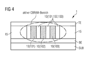
- a CBRAM memory device has memory cells 1 based on a variable in its active solid active electrolyte 13 or 131, 132, 133, embedded between a lower electrode BE ( B ottom E lectrode) and an upper electrode TE ( T op E lectrode) is switchable by applying a suitable electric field between these electrodes BE, TE between a low-resistance on-state and an off-high with a comparatively high resistance, and is characterized parallel to the solid-state electrolyte material 13, 131, 132, 133, a resistance material 10 or 101, 102, 103 is embedded in the active CBRAM region between the electrodes BE, TE.
- the memory cell 1 is structured by the embedding of the layer stack in a dielectric layer 15 for the isolation of adjacent cells.
- the resistance value of the resistance material can be adjusted, preferably to a value which lies between the resistance value of the active solid state electrolyte material in the on state and in the off state. While it is readily understood that the resistance of the resistive material can be adjusted by the choice of its resistivity, in the invention the resistance of the resistive material is further enhanced by a suitable layout of its layer and / or by a suitable layout of the solid state electrolyte material between the resistive materials Electrodes adjusted.
- the three preferred embodiments of the manufacturing method according to the invention described below use an aluminum oxide layer having nanopores acting as a positive mask or as a negative mask for structuring the resistance material and the layer of the solid electrolyte material between the electrodes.
- suitable electrolytes eg oxalic acid, sulfuric acid
- etching conditions such as etching time, electrical voltage, chemical concentration to homogeneous, hexagonal dense arrangements of pores with diameters down to 4 nm (cf.: H Masuda and K.
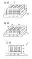
- FIGS. 1A-1G A first preferred embodiment of a manufacturing method according to the invention is described below with reference to FIGS. 1A-1G.
- the above-mentioned alumina nanoporous layer is used as a positive mask for patterning the resistance material for the parallel resistance and patterning the solid electrolyte material for the active layer.
- the metallization for the lower electrode BE is deposited on a substrate SUB and patterned.
- the electrode metal for example, tungsten, TiN, TiW, TiAlN or others can be used.
- a layer 10 of a parallel resistance conductive material is deposited on the lower electrode BE.
- an aluminum layer 11 is deposited and, according to FIG. 1D, anodically oxidized and thereby converted to a nanoporous Al 2 O 3 layer 12 with nanopores 14.
- the resulting nanopores 14 have a middle Diameter down to 4 nm and a typical diameter of approximately 10 nm.
- the resistance material of the layer 10 is first etched through the nanopores 14 of the Al 2 O 3 layer 12, so that nanopores are also formed in the layer 10 of the resistance material.
- a layer 13 of an active solid-state electrolyte material is deposited over the Al 2 O 3 layer 12, through its nanopores 14 and the nanopores formed in the resistance layer 10, so that nano-columns 131, 132 and 133 are embedded therein from the active solid electrolytic material.
- the active solid electrolyte material of the layer 13 and the nanocolumns 131-133 may be, for example, GeSe and Ag or GeS and Ag.
- the aluminum oxide layer 12 lying above the resistive layer 10 with the nanocolumns 131-133 of the active solid electrolyte material is subsequently removed, for example by lift-off or selective etching, the process state shown in FIG. 1F being established.
- the layers 12 and 13 above the layer 10 of the resistance material can be thinned back by CMP.
- the deposition of the metallization for the upper electrode TE takes place.
- the lateral structuring not shown in FIG. 1G, takes place by the embedding of the layer stack in a dielectric layer 15 for the insulation of adjacent cells (cf. Fig. 4). With this isolation and lateral structuring step, the CBRAM memory cell 1 is complete.
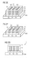
- FIGS. 2A - 2G A second preferred embodiment of a production method according to the invention of a CBRAM memory cell, in which the nanoporous aluminum oxide layer is used as a negative mask will be described below with reference to FIGS. 2A - 2G.
- the lower electrode BE deposited on a substrate SUB for example made of W, TiN, TiW, TiAlN or others, is assumed (FIG. 2A).
- the layer 13 of the active solid electrolyte material for example GeSe, GeS and Ag, is deposited over the lower electrode BE (FIG. 2B).
- an aluminum layer 11 is then deposited as shown in FIG.
- FIG. 2E the layer 13 of the active solid electrolyte material is selectively etched through the nanopores 14 formed in the aluminum oxide layer 12, so that nanopores are likewise produced in the layer 13 of the active material.
- a layer 10 of a resistance material for the parallel resistance is also deposited over the aluminum oxide layer 12, through its nanopores 14 and into the nanopores formed in the active layer 13. This is indicated by the columns of resistive material indicated at 101, 102 and 103.
- the resistivity and geometry of the resistive material determine R (out).
- the resistance material may be doped polysilicon or TiN, for example.
- the remaining aluminum oxide layer 12 is removed, for example by lift-off or selective etching.
- the material of the resistance layer 10 above the aluminum oxide layer 12 and in their nanopores is also removed.
- a thinning to the active layer 13 can also be performed here by CMP.
- the upper electrode TE is above the active layer 13 and the nanocolumns formed therein 101 - 103 of the resistance material deposited and structured.
- the CBRAM memory cell 1 produced according to the second preferred exemplary embodiment according to FIG. 2G is laterally structured by the embedding of the layer stack into a dielectric layer 15 as shown in FIG. 4 and thus isolated to adjacent cells.
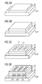
- the third preferred embodiment described with reference to Figures 3A-3G is an alternative to the process described with reference to Figures 2A-2G and utilizes a CMP step to pattern the active material.
- the starting point is again, according to FIG. 3A, the metallization deposited on a substrate SUB and structured for the lower electrode BE.
- the aluminum layer 11 is then deposited directly on the lower electrode BE according to FIG. 3B and anodically oxidized according to FIG. 3C to form an Al 2 O 3 layer 12 with the nanopores 14.
- the desired diameter of the nanopores 14 is here also about 10 nm.
- the layer 10 of resistance material is deposited over the aluminum oxide layer 12 and into its nanopores.
- the remaining aluminum oxide layer 12 is removed as shown in FIG. 3E.
- nano-columns 101, 102, 103 of the previously deposited resistance material 10 remain on the lower electrode BE.
- the layer 13 of the active solid electrolytic material is deposited and thinned back by CMP to the nanoscale 101-103 of the resistive material.
- the metallization for the upper electrode TE is then deposited over the active layer 13 as shown in FIG. 3G.
- the off-resistance R (out) is determined by the resistivity and resistive material 10 and the geometry of the nano-pillars 101-103 filled with the resistive material 10.
- the lateral structuring takes place by the embedding of the layer stack of the CBRAM memory cell in a dielectric layer 15 for the isolation of adjacent cells ( Figure 4).
- FIGS. 1A-1G, 2A-2G, 3A-3G and FIG Embedded electrode and an upper electrode which is characterized in that a resistance material is embedded parallel to the solid electrolyte material between the lower and upper electrode.
- a suitable electrolyte such as oxalic acid, sulfuric acid, anodized aluminum layer, depending on the choice of layer thickness and etching conditions, such as etching time, electrical voltage, chemical concentration of the electrolyte, homogeneous, hexagonal dense arrangements of nanopores with diameters down to to 4 nm.
- This aluminum oxide layer with the nanopores serves as a mask for the deposition of the active material and the material for the parallel resistance.
- the nanoporous alumina layer served as a positive mask, while in the second and third embodiments, it is used as a negative mask in FIGS. 2A-2G and 3A-3G, respectively.
- the off-resistance R (out) of the CBRAM cells 1 is defined by the layout and the manufacturing method.
- the off-resistance and the ratio R (off) / R (on) are thus no longer determined by the material properties alone but can be adapted to the needs of the evaluation logic and the desired application. This can avoid the disadvantages arising due to the high value of the off-resistance of the electrolyte material in the CBRAM cell.
- the The aging effect of the electrolyte material in the CBRAM cells are suppressed so that it is no longer measurable to the outside.
Landscapes
- Engineering & Computer Science (AREA)
- Manufacturing & Machinery (AREA)
- Semiconductor Memories (AREA)
Applications Claiming Priority (1)
| Application Number | Priority Date | Filing Date | Title |
|---|---|---|---|
| DE102004041894A DE102004041894B3 (de) | 2004-08-30 | 2004-08-30 | Speicherbauelement (CBRAM) mit Speicherzellen auf der Basis eines in seinem Widerstandswert änderbaren aktiven Festkörper-Elektrolytmaterials und Herstellungsverfahren dafür |
Publications (2)
| Publication Number | Publication Date |
|---|---|
| EP1630880A2 true EP1630880A2 (fr) | 2006-03-01 |
| EP1630880A3 EP1630880A3 (fr) | 2007-08-15 |
Family
ID=35311951
Family Applications (1)
| Application Number | Title | Priority Date | Filing Date |
|---|---|---|---|
| EP05107162A Withdrawn EP1630880A3 (fr) | 2004-08-30 | 2005-08-03 | Dispositif de mémoire (CBRAM) comportant des cellules de mémoire à base d'un matériau électrolyte solide à résistance variable et procédé pour sa fabrication |
Country Status (5)
| Country | Link |
|---|---|
| US (1) | US7737428B2 (fr) |
| EP (1) | EP1630880A3 (fr) |
| KR (1) | KR100843676B1 (fr) |
| CN (1) | CN1761064A (fr) |
| DE (1) | DE102004041894B3 (fr) |
Cited By (1)
| Publication number | Priority date | Publication date | Assignee | Title |
|---|---|---|---|---|
| WO2010012683A1 (fr) * | 2008-07-29 | 2010-02-04 | Commissariat A L'energie Atomique | Dispositif memoire et memoire cbram a fiabilite amelioree |
Families Citing this family (42)
| Publication number | Priority date | Publication date | Assignee | Title |
|---|---|---|---|---|
| KR100868321B1 (ko) | 2006-04-14 | 2008-11-11 | 재단법인서울대학교산학협력재단 | 다중 비트 상변화 메모리 소자의 단위 셀 |
| KR100833903B1 (ko) * | 2006-06-13 | 2008-06-03 | 광주과학기술원 | 비휘발성 기억소자, 그 제조방법 및 그 제조장치 |
| JP2008016115A (ja) * | 2006-07-05 | 2008-01-24 | Toshiba Corp | 不揮発性記憶装置 |
| US7515454B2 (en) * | 2006-08-02 | 2009-04-07 | Infineon Technologies Ag | CBRAM cell and CBRAM array, and method of operating thereof |
| KR100790894B1 (ko) * | 2006-11-15 | 2008-01-03 | 삼성전자주식회사 | 저항성 메모리 소자 |
| US20080278988A1 (en) * | 2007-05-09 | 2008-11-13 | Klaus Ufert | Resistive switching element |
| US8896100B2 (en) * | 2007-09-03 | 2014-11-25 | Sophia School Corporation | III nitride structure and method for manufacturing III nitride semiconductor fine columnar crystal |
| KR100885434B1 (ko) * | 2007-10-12 | 2009-02-24 | 연세대학교 산학협력단 | 저항변화 메모리 소자 및 그 제조방법 |
| US8659852B2 (en) | 2008-04-21 | 2014-02-25 | Seagate Technology Llc | Write-once magentic junction memory array |
| US7852663B2 (en) * | 2008-05-23 | 2010-12-14 | Seagate Technology Llc | Nonvolatile programmable logic gates and adders |
| US7855911B2 (en) * | 2008-05-23 | 2010-12-21 | Seagate Technology Llc | Reconfigurable magnetic logic device using spin torque |
| US8097902B2 (en) | 2008-07-10 | 2012-01-17 | Seagate Technology Llc | Programmable metallization memory cells via selective channel forming |
| US7881098B2 (en) | 2008-08-26 | 2011-02-01 | Seagate Technology Llc | Memory with separate read and write paths |
| US7985994B2 (en) | 2008-09-29 | 2011-07-26 | Seagate Technology Llc | Flux-closed STRAM with electronically reflective insulative spacer |
| US8169810B2 (en) | 2008-10-08 | 2012-05-01 | Seagate Technology Llc | Magnetic memory with asymmetric energy barrier |
| US8089132B2 (en) | 2008-10-09 | 2012-01-03 | Seagate Technology Llc | Magnetic memory with phonon glass electron crystal material |
| US8039913B2 (en) * | 2008-10-09 | 2011-10-18 | Seagate Technology Llc | Magnetic stack with laminated layer |
| US20100102405A1 (en) * | 2008-10-27 | 2010-04-29 | Seagate Technology Llc | St-ram employing a spin filter |
| US8045366B2 (en) * | 2008-11-05 | 2011-10-25 | Seagate Technology Llc | STRAM with composite free magnetic element |
| US8043732B2 (en) | 2008-11-11 | 2011-10-25 | Seagate Technology Llc | Memory cell with radial barrier |
| US7842938B2 (en) * | 2008-11-12 | 2010-11-30 | Seagate Technology Llc | Programmable metallization cells and methods of forming the same |
| US7750386B2 (en) * | 2008-11-12 | 2010-07-06 | Seagate Technology Llc | Memory cells including nanoporous layers containing conductive material |
| US7826181B2 (en) * | 2008-11-12 | 2010-11-02 | Seagate Technology Llc | Magnetic memory with porous non-conductive current confinement layer |
| US8289756B2 (en) | 2008-11-25 | 2012-10-16 | Seagate Technology Llc | Non volatile memory including stabilizing structures |
| CN101441913B (zh) * | 2008-12-25 | 2011-05-18 | 复旦大学 | 一种用于过电压保护的电阻开关器件 |
| TWI401796B (zh) * | 2008-12-30 | 2013-07-11 | Ind Tech Res Inst | 導通微通道記憶體元件及其製造方法 |
| US7826259B2 (en) * | 2009-01-29 | 2010-11-02 | Seagate Technology Llc | Staggered STRAM cell |
| US8487291B2 (en) * | 2009-01-30 | 2013-07-16 | Seagate Technology Llc | Programmable metallization memory cell with layered solid electrolyte structure |
| US7999338B2 (en) | 2009-07-13 | 2011-08-16 | Seagate Technology Llc | Magnetic stack having reference layers with orthogonal magnetization orientation directions |
| US9171613B2 (en) * | 2009-07-28 | 2015-10-27 | Hewlett-Packard Development Company, L.P. | Memristors with asymmetric electrodes |
| US8344428B2 (en) | 2009-11-30 | 2013-01-01 | International Business Machines Corporation | Nanopillar E-fuse structure and process |
| US9454997B2 (en) | 2010-12-02 | 2016-09-27 | Micron Technology, Inc. | Array of nonvolatile memory cells having at least five memory cells per unit cell, having a plurality of the unit cells which individually comprise three elevational regions of programmable material, and/or having a continuous volume having a combination of a plurality of vertically oriented memory cells and a plurality of horizontally oriented memory cells; array of vertically stacked tiers of nonvolatile memory cells |
| US8519373B2 (en) * | 2011-08-11 | 2013-08-27 | Micron Technology, Inc. | Memory cells |
| EP2756524A4 (fr) * | 2011-09-13 | 2015-06-03 | Adesto Technologies Corp | Dispositifs de commutation résistifs comprenant des électrodes en alliage et leurs procédés de formation |
| US8941089B2 (en) | 2012-02-22 | 2015-01-27 | Adesto Technologies Corporation | Resistive switching devices and methods of formation thereof |
| US9305643B2 (en) * | 2012-03-27 | 2016-04-05 | Adesto Technologies Corporation | Solid electrolyte based memory devices and methods having adaptable read threshold levels |
| KR101371438B1 (ko) * | 2012-06-20 | 2014-03-10 | 인텔렉추얼디스커버리 주식회사 | 서로 다른 종류의 전극을 이용한 멀티비트 저항변화 메모리 소자 및 그 제조방법 |
| US9627611B2 (en) | 2012-11-21 | 2017-04-18 | Micron Technology, Inc. | Methods for forming narrow vertical pillars and integrated circuit devices having the same |
| US9006700B2 (en) * | 2013-06-24 | 2015-04-14 | International Business Machines Corporation | Resistive memory with a stabilizer |
| KR101505495B1 (ko) | 2013-11-14 | 2015-03-24 | 한양대학교 산학협력단 | Cbram 소자 및 그 제조 방법 |
| US9306165B2 (en) | 2014-03-27 | 2016-04-05 | Micron Technology, Inc. | Replacement materials processes for forming cross point memory |
| US9831426B2 (en) | 2015-05-12 | 2017-11-28 | Iucf-Hyu | CBRAM device and manufacturing method thereof |
Family Cites Families (12)
| Publication number | Priority date | Publication date | Assignee | Title |
|---|---|---|---|---|
| DE19515492C1 (de) * | 1995-04-27 | 1996-10-24 | Werner Henze | Datenspeicher |
| US6705152B2 (en) * | 2000-10-24 | 2004-03-16 | Nanoproducts Corporation | Nanostructured ceramic platform for micromachined devices and device arrays |
| US6927411B2 (en) * | 2000-02-11 | 2005-08-09 | Axon Technologies Corporation | Programmable structure, an array including the structure, and methods of forming the same |
| US6566700B2 (en) * | 2001-10-11 | 2003-05-20 | Ovonyx, Inc. | Carbon-containing interfacial layer for phase-change memory |
| US6858482B2 (en) * | 2002-04-10 | 2005-02-22 | Micron Technology, Inc. | Method of manufacture of programmable switching circuits and memory cells employing a glass layer |
| US20040026682A1 (en) * | 2002-06-17 | 2004-02-12 | Hai Jiang | Nano-dot memory and fabricating same |
| US20040052117A1 (en) * | 2002-07-05 | 2004-03-18 | Hai Jiang | Fabrication of ultra-small memory elements |
| US7163837B2 (en) * | 2002-08-29 | 2007-01-16 | Micron Technology, Inc. | Method of forming a resistance variable memory element |
| US7242019B2 (en) * | 2002-12-13 | 2007-07-10 | Intel Corporation | Shunted phase change memory |
| US7307267B2 (en) * | 2002-12-19 | 2007-12-11 | Nxp B.V. | Electric device with phase change material and parallel heater |
| KR100615586B1 (ko) * | 2003-07-23 | 2006-08-25 | 삼성전자주식회사 | 다공성 유전막 내에 국부적인 상전이 영역을 구비하는상전이 메모리 소자 및 그 제조 방법 |
| TWI261915B (en) * | 2005-01-07 | 2006-09-11 | Ind Tech Res Inst | Phase change memory and fabricating method thereof |
-
2004
- 2004-08-30 DE DE102004041894A patent/DE102004041894B3/de not_active Expired - Fee Related
-
2005
- 2005-08-03 EP EP05107162A patent/EP1630880A3/fr not_active Withdrawn
- 2005-08-29 US US11/214,692 patent/US7737428B2/en not_active Expired - Fee Related
- 2005-08-29 CN CNA2005100976378A patent/CN1761064A/zh active Pending
- 2005-08-30 KR KR1020050080129A patent/KR100843676B1/ko not_active Expired - Fee Related
Cited By (3)
| Publication number | Priority date | Publication date | Assignee | Title |
|---|---|---|---|---|
| WO2010012683A1 (fr) * | 2008-07-29 | 2010-02-04 | Commissariat A L'energie Atomique | Dispositif memoire et memoire cbram a fiabilite amelioree |
| FR2934711A1 (fr) * | 2008-07-29 | 2010-02-05 | Commissariat Energie Atomique | Dispositif memoire et memoire cbram a fiablilite amelioree. |
| US9082965B2 (en) | 2008-07-29 | 2015-07-14 | Commissariat A L'energie Atomique Et Aux Energies Alternatives | Memory device and CBRAM memory with improved reliability |
Also Published As
| Publication number | Publication date |
|---|---|
| DE102004041894B3 (de) | 2006-03-09 |
| US20060060832A1 (en) | 2006-03-23 |
| KR100843676B1 (ko) | 2008-07-04 |
| KR20060050833A (ko) | 2006-05-19 |
| CN1761064A (zh) | 2006-04-19 |
| EP1630880A3 (fr) | 2007-08-15 |
| US7737428B2 (en) | 2010-06-15 |
Similar Documents
| Publication | Publication Date | Title |
|---|---|---|
| DE102004041894B3 (de) | Speicherbauelement (CBRAM) mit Speicherzellen auf der Basis eines in seinem Widerstandswert änderbaren aktiven Festkörper-Elektrolytmaterials und Herstellungsverfahren dafür | |
| DE102005005938B4 (de) | Resistives Speicherelement mit verkürzter Löschzeit, Verfahren zur Herstellung und Speicherzellen-Anordnung | |
| DE102004007633B4 (de) | Speicherzelle, Halbleiter-Speicherbauelement und Verfahren zur Herstellung einer Speicherzelle | |
| DE102008016522B4 (de) | Phasenwechselspeicherzelle mit Phasenwechsel-Speichermaterial mit begrenztem Widerstand, Verfahren zur Herstellung einer deratigen Speicherzelle und integrierte Schaltung mit entsprechender Speicherzelle | |
| DE69724478T2 (de) | Verfahren zur Herstellung eines kleinflächigen Kontakts zwischen Elektroden | |
| DE60126310T2 (de) | Punktkontaktarray, Not-Schaltung und elektronische Schaltung damit | |
| DE102009006402B4 (de) | Resistiv arbeitende Speicherzelle, resistiv arbeitende Speichervorrichtung und Verfahren zur Herstellung derselben | |
| DE112012003382B4 (de) | Mikroelektronische Einheit, Zellstruktur mit mikroelektronischer Einheit, Speicheranordnung und Verfahren zum Betrieb einer Anordnung | |
| EP1687855B1 (fr) | Memoire a semi-conducteurs integres et procede pour produire une memoire a semi-conducteurs integres | |
| DE102014108256A1 (de) | Phasenänderungs-Speicherzellen | |
| DE102004031135A1 (de) | Resistives Halbleiterelement basierend auf einem Festkörperionenleiter | |
| DE112014002344T5 (de) | Hochkonsistenter und energiesparender resistiver speicher und verfahren zu dessen herstellung | |
| DE102004056973A1 (de) | Herstellungsverfahren mit selbstjustierter Anordnung von Festkörperelektrolyt-Speicherzellen minimaler Strukturgröße | |
| DE112021005520B4 (de) | Nicht-flüchtige speicherzellen mit widerstands-drift-abschwächung und verfahren zur herstellung | |
| DE102004018715B3 (de) | Speicherzelle zum Speichern einer Information, Speicherschaltung sowie Verfahren zum Herstellen einer Speicherzelle | |
| DE102004011431B4 (de) | Verfahren zum Herstellen eines nicht flüchtigen Halbleiterspeichers | |
| DE102004041893B4 (de) | Verfahren zur Herstellung von Speicherbauelementen (PCRAM) mit Speicherzellen auf der Basis einer in ihrem Phasenzustand änderbaren Schicht | |
| DE112006000612T5 (de) | Nichtflüchtiges Speicherelement | |
| DE102004037450B4 (de) | Verfahren zum Betrieb eines Schalt-Bauelements | |
| DE102005001253A1 (de) | Speicherzellenanordnung, Verfahren zu deren Herstellung und Halbleiterspeichereinrichtung | |
| DE102004040752A1 (de) | Integrierte Speicheranordnung auf der Basis resistiver Speicherzellen und Herstellungsverfahren dafür | |
| DE102004046804B4 (de) | Resistiv schaltender Halbleiterspeicher | |
| DE102021109728A1 (de) | Schwellenspannungsmoduliertes speicherbauelement mit variabler kapazität und herstellungsverfahren dafür | |
| DE102005016244A1 (de) | Speicherzelle, Speichereinrichtung und Verfahren zu deren Herstellung | |
| DE112023003814T5 (de) | Resistiver speicher mit widerstandsausbreitungsschicht |
Legal Events
| Date | Code | Title | Description |
|---|---|---|---|
| PUAI | Public reference made under article 153(3) epc to a published international application that has entered the european phase |
Free format text: ORIGINAL CODE: 0009012 |
|
| AK | Designated contracting states |
Kind code of ref document: A2 Designated state(s): AT BE BG CH CY CZ DE DK EE ES FI FR GB GR HU IE IS IT LI LT LU LV MC NL PL PT RO SE SI SK TR |
|
| AX | Request for extension of the european patent |
Extension state: AL BA HR MK YU |
|
| PUAL | Search report despatched |
Free format text: ORIGINAL CODE: 0009013 |
|
| AK | Designated contracting states |
Kind code of ref document: A3 Designated state(s): AT BE BG CH CY CZ DE DK EE ES FI FR GB GR HU IE IS IT LI LT LU LV MC NL PL PT RO SE SI SK TR |
|
| AX | Request for extension of the european patent |
Extension state: AL BA HR MK YU |
|
| 17P | Request for examination filed |
Effective date: 20080125 |
|
| 17Q | First examination report despatched |
Effective date: 20080221 |
|
| AKX | Designation fees paid |
Designated state(s): DE FR |
|
| STAA | Information on the status of an ep patent application or granted ep patent |
Free format text: STATUS: THE APPLICATION IS DEEMED TO BE WITHDRAWN |
|
| 18D | Application deemed to be withdrawn |
Effective date: 20090609 |