EP1632025B1 - Verbesserte lastregelung und versorgungsspannungsunterdrückung unter verwendung eines transkonduktanz- und eines operationsverstärkers in tandemschaltung - Google Patents
Verbesserte lastregelung und versorgungsspannungsunterdrückung unter verwendung eines transkonduktanz- und eines operationsverstärkers in tandemschaltung Download PDFInfo
- Publication number
- EP1632025B1 EP1632025B1 EP04754523A EP04754523A EP1632025B1 EP 1632025 B1 EP1632025 B1 EP 1632025B1 EP 04754523 A EP04754523 A EP 04754523A EP 04754523 A EP04754523 A EP 04754523A EP 1632025 B1 EP1632025 B1 EP 1632025B1
- Authority
- EP
- European Patent Office
- Prior art keywords
- source
- coupled
- drain
- gate
- amplifier
- Prior art date
- Legal status (The legal status is an assumption and is not a legal conclusion. Google has not performed a legal analysis and makes no representation as to the accuracy of the status listed.)
- Expired - Lifetime
Links
- 239000003990 capacitor Substances 0.000 claims description 6
- 230000003071 parasitic effect Effects 0.000 claims description 3
- 230000005669 field effect Effects 0.000 claims 4
- 238000010586 diagram Methods 0.000 description 12
- 230000008901 benefit Effects 0.000 description 7
- 238000005516 engineering process Methods 0.000 description 3
- 230000004048 modification Effects 0.000 description 3
- 238000012986 modification Methods 0.000 description 3
- 230000003068 static effect Effects 0.000 description 2
- HBBGRARXTFLTSG-UHFFFAOYSA-N Lithium ion Chemical compound [Li+] HBBGRARXTFLTSG-UHFFFAOYSA-N 0.000 description 1
- 238000013459 approach Methods 0.000 description 1
- 230000007812 deficiency Effects 0.000 description 1
- 230000001419 dependent effect Effects 0.000 description 1
- 229910001416 lithium ion Inorganic materials 0.000 description 1
- 230000001105 regulatory effect Effects 0.000 description 1
Images


Classifications
-
- H—ELECTRICITY
- H03—ELECTRONIC CIRCUITRY
- H03F—AMPLIFIERS
- H03F3/00—Amplifiers with only discharge tubes or only semiconductor devices as amplifying elements
- H03F3/45—Differential amplifiers
-
- H—ELECTRICITY
- H03—ELECTRONIC CIRCUITRY
- H03F—AMPLIFIERS
- H03F3/00—Amplifiers with only discharge tubes or only semiconductor devices as amplifying elements
- H03F3/45—Differential amplifiers
- H03F3/45071—Differential amplifiers with semiconductor devices only
- H03F3/45076—Differential amplifiers with semiconductor devices only characterised by the way of implementation of the active amplifying circuit in the differential amplifier
- H03F3/45179—Differential amplifiers with semiconductor devices only characterised by the way of implementation of the active amplifying circuit in the differential amplifier using MOSFET transistors as the active amplifying circuit
- H03F3/4521—Complementary long tailed pairs having parallel inputs and being supplied in parallel
Definitions
- the present invention relates generally to operational amplifier circuits, and more particularly to high gain and high bandwidth operational amplifier circuits.
- Electronic regulator loops e . g ., voltage, etc .
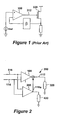
- a power output device controlled by an operational amplifier in a feed-back loop (see Figure 1 ).
- both high gain and wide bandwidth are required in the loop.
- High gain improves the output line, e . g ., voltage, regulation and wide bandwidth improves the response time to a sudden load change.
- high gain and wide bandwidth operational amplifier circuits pose stability problems.
- Existing approaches to obtaining stable high gain regulators having good regulation have been the use of gain boosting operational amplifier circuits, and/or nested operational amplifier circuits.
- the stability of the gain boosting operational amplifier circuits depends upon the external load characteristics.
- the nested operational amplifier circuit are stable because they have limited bandwidth, and thus produce poor load regulation.
- a wide-bandwidth operational amplifier is known from US2002/0003441 . Furthermore, US2003/0085763 discloses an electronic output stage.
- an electronic amplifier circuit that enables improved line and load regulation at the same time.
- this electronic amplifier will achieve good stability while maintaining high gain (reduced loop error) and wide bandwidth (fast response to a load change.
- an electronic amplifier circuit can be provided having high open-loop gain and high gain-bandwidth while maintaining stability over a wide range of operating parameters.
- the invention electronic amplifier circuit may be effectively used in battery chargers, DC to DC converters, low drop out (LDO) voltage regulators, and the like.
- the invention electronic amplifier circuit allows highly stabile and precisely regulated output voltages.
- the invention electronic amplifier circuit comprises an operational transconductance amplifier (OTA) coupled with an operational amplifier (OA) to produce a wide-bandwidth, high-gain amplifier circuit that may be used in a closed loop voltage regulator having both wide bandwidth and high gain, and is stable over all operating conditions.
- the OA may be, for example, a cascade of two OTA (two-stage OTA), a three stage amplifier and the like.
- the OA has a high gain but limited bandwidth.
- the OTA has a large (wide) bandwidth but limited gain. Thus, the OTA provides high bandwidth while the OA provides high open-loop gain.
- Figure 2 depicts an OTA 100 and an OA 200 coupled together to achieve both high bandwidth and high open loop gain.
- the OTA 100 has high bandwidth and is in the main signal path. However, the OTA 100 has low gain, therefore it may induce a significant static error in a closed loop configuration.
- the OA 200 may be used to monitor the offset of the high bandwidth OTA 100 as a function of the differential voltage between the input nodes 114 and 116.
- the OA 200 may be connected in such a way that in a closed loop configuration the offset of the OTA 100 is substantially cancelled.
- a low frequency static error is considered as an offset by the OA 200 and thus is cancelled or reduced to a very low level.
- a technical advantage of the invention is good stability over a widely varying range of loads and rapidly changing load characteristics. Yet another technical advantage is reduced power consumption for improved operating characteristics. Another technical advantage is increased gain-bandwidth.
- the high-gain, wide-bandwidth operational amplifier 300 comprises an operational transconductance amplifier (OTA) 100 and a two-stage operational amplifier 200 (amplifier 200 also may be a three stage amplifier and the like) coupled together as more fully described hereinafter (see Figures 3, 4 , 5 and 6 ).
- the amplifier 300 is stable over a wide range and nature of the load impedance 320, and preferably has a phase margin of at least 70 degrees, preferably over a load capacitance of from about one picofarad to about ten nanofarads.
- FIG. 3 depicted is a schematic diagram of an exemplary embodiment of an operational transconductance amplifier (OTA) that may be used for the OTA 100 depicted in Figure 2 .
- the OTA 100 has a current output 112 controlled by a differential input voltage between inputs 114 and 116.
- the output current is proportional to the voltage difference between the differential inputs 114 and 116 and the transconductance (g M ) of the OTA 100.
- the inputs 114 and 116 are coupled to the gates of transistors 106 and 108, respectively, and are adapted to receive differential voltage inputs.
- Transistor 102 is a current mirror to transistor 104.
- the drain of transistor 108 is connected to the input 118 of the current mirror formed by transistors 102 and 104.
- the drains of transistors 104 and 106 form the current output 112.
- Current source 130 is connected between transistors 106 and 108, and common or ground 110.
- Transistors 102 and 104 are also connected to a positive supply voltage, V DD , 120.
- the OTA 100 is characterized as having limited gain, but a wide (large) bandwidth.
- the current source 130 may also be a constant current source.
- FIG. 4 depicted is a schematic block diagram of an exemplary embodiment of a two-stage operational amplifier that may be used for the two-stage operational amplifier 200 depicted in Figure 2 .
- the two-stage operational amplifier 200 comprises cascade connected OTA 201 and OTA 202, and a compensation capacitor 203.
- the compensation capacitor 203 provides phase stability at both high and low gains.
- the two-stage operational amplifier 200 may be characterized as having high gain, but a limited bandwidth. It is contemplated and within the scope of the invention that the two-stage operational amplifier 200 also may be comprised of a three stage amplifier and the like (not shown).
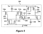
- FIG. 5 depicted is a schematic diagram of an exemplary embodiment of a two stage operational amplifier that may be used for the two-stage operational amplifier 200 shown in Figure 4 .
- a P-type differential input pair may be used for the first OTA 201 (transistors 216, 218, 212 and 214) while the OTA 202 (transistors 222, 224, 226 and 228) may be similar to the OTA 100 shown in Figure 3 .
- the inputs 114a and 116a of the first OTA 201 are coupled to the gates of transistors 216 and 218, respectively, and are adapted to receive differential voltage inputs.
- Current source 230 is connected between transistors 216 and 218, and the positive supply voltage, V DD , 120.
- Transistor 212 is a current mirror to transistor 214.
- the drain of transistor 218 is connected to the input 213 of the current mirror formed by transistors 212 and 214.
- the drains of transistors 214 and 216 form the current output 211 of the first OTA 201.
- Transistors 212 and 214 are also connected to common or ground 110a.
- Nodes 211 and 213 are coupled to the gates of transistors 226 and 228, respectively, and are adapted to receive differential voltage inputs.
- Current source 240 is connected between transistors 226 and 228, and common or ground 110a.
- Transistor 222 is a current mirror to transistor 224.
- the drain of transistor 228 is connected to the input 221 of the current mirror formed by transistors 222 and 224.
- the drains of transistors 224 and 226 form the current output 118a of the second OTA 202.
- Transistors 222 and 224 are also connected to the positive supply voltage, V DD , 120.
- the compensation capacitor 203 is connected between nodes 211 and 213.
- a transistor 204 may be used to clamp voltage swing.
- FIG. 5 depicted is a schematic block diagram of a high-gain, wide-bandwidth operational amplifier, according to an exemplary embodiment of the invention.
- the impedance 420 is proportional to the reciprocal of the sum of the transconductance of transistor 302 and j ⁇ Cp, were Cp is the parasitic capacitance depicted as capacitor 322 in Figure 5 .
- the amplifier 300 is stable over a wide range and nature of the load impedance 320, and preferably has a phase margin of at least 70 degrees, preferably over a load capacitance of from about one picofarad to about ten nanofarads.
- FIG. 6 depicted is a schematic diagram of an exemplary embodiment of a high-gain, wide-bandwidth operational amplifier, according to a combination of the circuits shown in Figures 3, 4 and 5 .
- the amplifier 300 may comprise the OTA 100 shown in Figure 3 in combination with the two-stage operational amplifier 200 shown in Figures 4 and 5 (amplifier 200 also may be a three stage amplifier and the like).
- the output 112 of the amplifier 300 is coupled to a load impedance 320, e.g., the output power device.
- Inputs 114 and 116 are adapted to receive a differential voltage input signal.
- the inputs 114 and 116 are coupled to the gates of transistors 106 and 108, respectively, and are adapted to receive the differential voltage inputs.
- Transistor 102 is a current mirror to transistor 104. The junction of transistors 104 and 106 form the current output 112. Current source 130 is connected between transistors 106 and 108, and common or ground 110. Transistors 102 and 104 are also connected to a positive supply voltage, V DD , 120. The output 118a of the amplifier 200 is coupled to the gates of the transistors 302 and 304, and the inputs 114a and 116a of the amplifier 200 are coupled to the inputs 114 and 116, respectively.
- An impedance 420 ( Figure 2 ) is proportional to the reciprocal of the sum of the transconductance of transistor 102 and j ⁇ Cp, were Cp is a parasitic capacitance depicted as capacitor 322.
- Amplifier 200 depicted in Figure 5 , alternatively, may be differentially coupled to nodes 118 and 112. However, the connections of the amplifier 200 depicted in Figure 5 may reduce the requirements on the dynamic range of the amplifier 200 output. Moreover it allows use of the node 118 as an extra input that may be used to perform the current limitation and/or temperature protection of a voltage regulator implemented with the exemplary embodiments disclosed herein.
- the invention amplifier 300 may be fabricated on an integrated circuit (not shown).
- the integrated circuit may also comprise other analog and/or digital circuits, including but not limited to a digital processor.
- the digital processor may be a microprocessor, a microcontroller, a programmable logic array (PLA), an application specific integrated circuit (ASIC) and the like. It is contemplated and within the scope of the invention that the amplifier 300 may be used advantageously in voltage and current regulation applications, battery chargers, power management, low dropout power regulators, DC to DC converters and the like.
- the current sources may be a constant current source, a PTAT current source, an inverse PTAT current source, and the like.
Landscapes
- Engineering & Computer Science (AREA)
- Power Engineering (AREA)
- Amplifiers (AREA)
- Tone Control, Compression And Expansion, Limiting Amplitude (AREA)
- Networks Using Active Elements (AREA)
Claims (10)
- Elektronischer Verstärker, mit einem Transkonduktanzoperationsverstärker (OTA) (100), der Differenzeingänge und einen Ausgang aufweist; und einem Operationsverstärker (OA) (200), der Differenzeingänge und einen Ausgang aufweist, wobei die Differenzeingänge des OA (200) parallel geschaltet sind mit den Differenzeingängen des OTA (100) und der Ausgang des OA (200) mit dem OTA (100) verbunden ist, um so den Offset in dem OTA (100) zu minimieren, wobei der OTA (100) aufweist:einen ersten Transistor (102), der einen ersten Gateanschluss, einen ersten Sourceanschluss und einen ersten Drainanschluss aufweist;einen zweiten Transistor (104), der einen zweiten Gateanschluss, einen zweiten Sourceanschluss und einen zweiten Drainanschluss aufweist;einen dritten Transistor (106), der einen dritten Gateanschluss, einen dritten Sourceanschluss und einen dritten Drainanschluss aufweist;einen vierten Transistor (108), der einen vierten Gateanschluss, einen vierten Sourceanschluss und einen vierten Drainanschluss aufweist; undeine erste Stromquelle (130);wobei:die erste Stromquelle (130) zwischen einer Spannungsquelle und den dritten und vierten Sourceanschlüssen verbunden ist,die dritten und vierten Sourceanschlüsse miteinander verbunden sind,der vierte Drainanschluss mit dem ersten Drainanschluss und den ersten und zweiten Gateanschlüssen verbunden ist,der zweite Drainanschluss mit dem dritten Drainanschluss verbunden ist und die zweiten und dritten Drainanschlüsse als ein Ausgang des elektronischen Verstärkers ausgebildet sind,die ersten und zweiten Sourceanschlüsse mit einer Spannungsquelle verbunden sind,der dritte Gateanschluss als ein erster Differenzeingang des elektronischen Verstärkers ausgebildet ist,die vierte Gateanschluss als ein zweiter Differenzeingang des elektronischen Verstärkers ausgebildet ist, undwobei der Ausgang des OA (200) mit dem ersten Drainanschluss und den ersten und zweiten Gateanschlüssen des OTA (100) verbunden ist, um so den Offset in dem OTA (100) zu minimieren.
- Elektronischer Verstärker nach Anspruch 1, der weiterhin eine parasitäre Kapazität zwischen den ersten und zweiten Gateanschlüssen und der Spannungsquelle aufweist.
- Elektronischer Verstärker nach Anspruch 1 oder 2, der weiterhin einen Steuereingang zur Strombegrenzung aufweist, der mit den ersten und vierten Drainanschlüssen und den ersten und zweiten Gateanschlüssen verbunden ist.
- Elektronischer Verstärker gemäß einem der vorherigen Ansprüche, der weiterhin einen Steuereingang zum Temperaturschutz aufweist, der mit den ersten und vierten Drainanschlüssen und den ersten und zweiten Gateanschlüssen verbunden ist.
- Elektronischer Verstärker nach Anspruch 4, wobei die ersten und zweiten Transistoren p-Kanal Feldeffekttransistoren sind, und die dritten und vierten Transistoren n-Kanal Feldeffekttransistoren sind.
- Elektronischer Verstärker nach Anspruch 4, wobei die erste Stromquelle ausgewählt ist aus der Gruppe die besteht aus einer Konstantstromquelle, einer Stromquelle die proportional zur absoluten Temperatur (PTAT) ist, und einer inversen PTAT Stromquelle.
- Elektronischer Verstärker gemäß einem der vorherigen Ansprüche, wobei der OA aufweist:einen fünften Transistor (218), der einen fünften Gateanschluss, einen fünften Sourceanschluss und einen fünften Drainanschluss aufweist;einen sechsten Transistor (216), der einen sechsten Gateanschluss, einen sechsten Sourceanschluss und einen sechsten Drainanschluss aufweist;einen siebten Transistor (214), der einen siebten Gateanschluss, einen siebten Sourceanschluss und einen siebten Drainanschluss aufweist;einen achten Transistor (212), der einen achten Gateanschluss, einen achten Sourceanschluss und einen achten Drainanschluss aufweist; undeine zweite Stromquelle (230);wobei:die zweite Stromquelle (230) zwischen der Spannungsquelle und den fünften und sechsten Drainanschlüssen verbunden ist,die fünften und sechsten Drainanschlüsse miteinander verbunden sind,der fünfte Sourceanschluss mit dem achten Drainanschluss und den siebten und achten Gateanschlüssen verbunden ist,der sechste Sourceanschluss mit dem siebten Drainanschluss verbunden ist,die siebten und achten Sourceanschlüsse mit der Spannungsquelle verbunden sind,der fünfte Gateanschluss mit dem vierten Gateanschluss verbunden ist,der sechste Gateanschluss mit dem zweiten Gateanschluss verbunden ist, unddie sechsten und siebten Drainanschlüsse als ein Stromausgang ausgebildet sind.
- Elektronischer Verstärker nach Anspruch 7, der einen Kompensationskondensator (203) aufweist, der zwischen den fünften und sechsten Sourceanschlüssen verbunden ist.
- Elektronischer Verstärker nach Anspruch 7, wobei die fünften und sechsten Transistoren (218, 216) n-Kanal Feldeffekttransistoren sind, und die siebten und achten Transistoren (214, 212) p-Kanal Feldeffekttransistoren sind.
- Elektronischer Verstärker nach Anspruch 7, wobei die zweite Stromquelle (230) ausgewählt ist aus der Gruppe die besteht aus einer Konstantstromquelle, einer PTAT Stromquelle, und einer inversen PTAT Stromquelle.
Applications Claiming Priority (3)
| Application Number | Priority Date | Filing Date | Title |
|---|---|---|---|
| US47714303P | 2003-06-09 | 2003-06-09 | |
| US10/857,332 US7091785B2 (en) | 2003-06-09 | 2004-05-28 | Load and line regulation using operational transconductance amplifier and operational amplifier in tandem |
| PCT/US2004/017930 WO2004112243A1 (en) | 2003-06-09 | 2004-06-07 | Improved load and line regulation using operational transconductance amplifier and operational amplifier in tandem |
Publications (2)
| Publication Number | Publication Date |
|---|---|
| EP1632025A1 EP1632025A1 (de) | 2006-03-08 |
| EP1632025B1 true EP1632025B1 (de) | 2008-11-05 |
Family
ID=33493614
Family Applications (1)
| Application Number | Title | Priority Date | Filing Date |
|---|---|---|---|
| EP04754523A Expired - Lifetime EP1632025B1 (de) | 2003-06-09 | 2004-06-07 | Verbesserte lastregelung und versorgungsspannungsunterdrückung unter verwendung eines transkonduktanz- und eines operationsverstärkers in tandemschaltung |
Country Status (7)
| Country | Link |
|---|---|
| US (1) | US7091785B2 (de) |
| EP (1) | EP1632025B1 (de) |
| KR (1) | KR100819862B1 (de) |
| CN (1) | CN100539403C (de) |
| AT (1) | ATE413724T1 (de) |
| DE (1) | DE602004017602D1 (de) |
| WO (1) | WO2004112243A1 (de) |
Families Citing this family (13)
| Publication number | Priority date | Publication date | Assignee | Title |
|---|---|---|---|---|
| JP4871590B2 (ja) * | 2005-12-28 | 2012-02-08 | パナソニック株式会社 | トランスコンダクタを用いた積分器及びフィルタ回路 |
| US7595691B2 (en) * | 2007-09-04 | 2009-09-29 | Himax Technologies Limited | Pre-amplifier for a receiver and a method therefor |
| US7760019B2 (en) * | 2008-03-04 | 2010-07-20 | Micron Technology, Inc. | Adaptive operational transconductance amplifier load compensation |
| CN102510267B (zh) * | 2011-12-28 | 2015-01-14 | 上海贝岭股份有限公司 | 一种二级运算放大器电路 |
| CN102707757B (zh) * | 2012-06-05 | 2014-07-16 | 电子科技大学 | 一种动态电荷放电电路以及集成该电路的ldo |
| TWI470394B (zh) * | 2012-12-13 | 2015-01-21 | Issc Technologies Corp | 電壓產生器 |
| KR101596568B1 (ko) | 2014-03-13 | 2016-02-29 | 충북대학교 산학협력단 | 입력 공통모드 어답터를 구비하는 연산 트랜스컨덕턴스 증폭기 회로 |
| US9874893B2 (en) * | 2015-05-27 | 2018-01-23 | Analog Devices, Inc. | Self-biased multiple cascode current mirror circuit |
| CN105094199B (zh) * | 2015-07-08 | 2017-03-15 | 江阴市飞凌科技有限公司 | 低噪音低功耗ldo电路 |
| US10013009B2 (en) | 2015-09-25 | 2018-07-03 | Texas Instruments Incorporated | Fault tolerant voltage regulator |
| US10756676B2 (en) | 2018-10-17 | 2020-08-25 | Analog Devices Global Unlimited Company | Amplifier systems for driving a wide range of loads |
| GB202107532D0 (en) * | 2021-05-27 | 2021-07-14 | Ams Sensors Singapore Pte Ltd | Circuit for device temperature protection |
| CN116339426A (zh) * | 2021-12-24 | 2023-06-27 | 立锜科技股份有限公司 | 阻抗追踪电路以及集成电路 |
Family Cites Families (6)
| Publication number | Priority date | Publication date | Assignee | Title |
|---|---|---|---|---|
| US4333058A (en) * | 1980-04-28 | 1982-06-01 | Rca Corporation | Operational amplifier employing complementary field-effect transistors |
| US5625317A (en) | 1994-08-08 | 1997-04-29 | Texas Instruments Incorporated | Tuning method for integrated continuous-time filters |
| US5880634A (en) * | 1997-03-21 | 1999-03-09 | Plato Labs, Inc. | Wide band-width operational amplifier |
| WO2000003476A1 (en) | 1998-07-13 | 2000-01-20 | Steensgaard Madsen Jesper | Wide-bandwidth operational amplifier |
| DE10016445C2 (de) | 2000-03-29 | 2002-03-28 | Infineon Technologies Ag | Elektronische Ausgangsstufe |
| US6437645B1 (en) * | 2001-02-15 | 2002-08-20 | Texas Instruments Incorporated | Slew rate boost circuitry and method |
-
2004
- 2004-05-28 US US10/857,332 patent/US7091785B2/en not_active Expired - Lifetime
- 2004-06-07 DE DE602004017602T patent/DE602004017602D1/de not_active Expired - Lifetime
- 2004-06-07 WO PCT/US2004/017930 patent/WO2004112243A1/en not_active Ceased
- 2004-06-07 EP EP04754523A patent/EP1632025B1/de not_active Expired - Lifetime
- 2004-06-07 AT AT04754523T patent/ATE413724T1/de not_active IP Right Cessation
- 2004-06-07 CN CNB2004800158950A patent/CN100539403C/zh not_active Expired - Lifetime
- 2004-06-07 KR KR1020057023558A patent/KR100819862B1/ko not_active Expired - Lifetime
Also Published As
| Publication number | Publication date |
|---|---|
| WO2004112243A1 (en) | 2004-12-23 |
| US7091785B2 (en) | 2006-08-15 |
| KR20060035617A (ko) | 2006-04-26 |
| KR100819862B1 (ko) | 2008-04-07 |
| US20040246052A1 (en) | 2004-12-09 |
| EP1632025A1 (de) | 2006-03-08 |
| CN100539403C (zh) | 2009-09-09 |
| ATE413724T1 (de) | 2008-11-15 |
| DE602004017602D1 (de) | 2008-12-18 |
| CN1802788A (zh) | 2006-07-12 |
Similar Documents
| Publication | Publication Date | Title |
|---|---|---|
| US7166991B2 (en) | Adaptive biasing concept for current mode voltage regulators | |
| US6677735B2 (en) | Low drop-out voltage regulator having split power device | |
| US8289009B1 (en) | Low dropout (LDO) regulator with ultra-low quiescent current | |
| Maity et al. | A hybrid-mode operational transconductance amplifier for an adaptively biased low dropout regulator | |
| US20090128107A1 (en) | Low Dropout Voltage Regulator | |
| US7612547B2 (en) | Series voltage regulator with low dropout voltage and limited gain transconductance amplifier | |
| US9553548B2 (en) | Low drop out voltage regulator and method therefor | |
| US10175707B1 (en) | Voltage regulator having feedback path | |
| US5789981A (en) | High-gain operational transconductance amplifier offering improved bandwidth | |
| US7091785B2 (en) | Load and line regulation using operational transconductance amplifier and operational amplifier in tandem | |
| CN108445959B (zh) | 一种可选接片外电容的低压差线性稳压器 | |
| CN105652946A (zh) | 一种自适应偏置的低负载调整率低压差线性稳压器 | |
| Kamel et al. | A hybrid NMOS/PMOS capacitor-less low-dropout regulator with fast transient response for SoC applications | |
| US20240319756A1 (en) | Low dropout regulator | |
| US6414552B1 (en) | Operational transconductance amplifier with a non-linear current mirror for improved slew rate | |
| CN108268078B (zh) | 一种低成本低功耗的低压差线性稳压器 | |
| Hwang et al. | A 0.35 μm CMOS sub-1V low-quiescent-current low-dropout regulator | |
| US6933708B2 (en) | Voltage regulator with reduced open-loop static gain | |
| CN114564067A (zh) | 一种具有高电源抑制比的低压差线性稳压器 | |
| Giustolisi et al. | A 50‐mA 1‐nF Low‐Voltage Low‐Dropout Voltage Regulator for SoC Applications | |
| US20020005757A1 (en) | Fully differential operational amplifier of the folded cascode type | |
| Cheng et al. | A low power high area-efficiency NMOS LDO with fast adaptive bias | |
| Kamel et al. | A hybrid NMOS/PMOS low-dropout regulator with fast transient response for SoC applications | |
| CN210005943U (zh) | 一种输出电压可调的基准电压源 | |
| US6831501B1 (en) | Common-mode controlled differential gain boosting |
Legal Events
| Date | Code | Title | Description |
|---|---|---|---|
| PUAI | Public reference made under article 153(3) epc to a published international application that has entered the european phase |
Free format text: ORIGINAL CODE: 0009012 |
|
| 17P | Request for examination filed |
Effective date: 20051207 |
|
| AK | Designated contracting states |
Kind code of ref document: A1 Designated state(s): AT BE BG CH CY CZ DE DK EE ES FI FR GB GR HU IE IT LI LU MC NL PL PT RO SE SI SK TR |
|
| 17Q | First examination report despatched |
Effective date: 20060308 |
|
| DAX | Request for extension of the european patent (deleted) | ||
| GRAP | Despatch of communication of intention to grant a patent |
Free format text: ORIGINAL CODE: EPIDOSNIGR1 |
|
| GRAS | Grant fee paid |
Free format text: ORIGINAL CODE: EPIDOSNIGR3 |
|
| GRAA | (expected) grant |
Free format text: ORIGINAL CODE: 0009210 |
|
| AK | Designated contracting states |
Kind code of ref document: B1 Designated state(s): AT BE BG CH CY CZ DE DK EE ES FI FR GB GR HU IE IT LI LU MC NL PL PT RO SE SI SK TR |
|
| REG | Reference to a national code |
Ref country code: GB Ref legal event code: FG4D |
|
| REG | Reference to a national code |
Ref country code: CH Ref legal event code: EP |
|
| REG | Reference to a national code |
Ref country code: IE Ref legal event code: FG4D |
|
| REF | Corresponds to: |
Ref document number: 602004017602 Country of ref document: DE Date of ref document: 20081218 Kind code of ref document: P |
|
| PG25 | Lapsed in a contracting state [announced via postgrant information from national office to epo] |
Ref country code: AT Free format text: LAPSE BECAUSE OF FAILURE TO SUBMIT A TRANSLATION OF THE DESCRIPTION OR TO PAY THE FEE WITHIN THE PRESCRIBED TIME-LIMIT Effective date: 20081105 Ref country code: ES Free format text: LAPSE BECAUSE OF FAILURE TO SUBMIT A TRANSLATION OF THE DESCRIPTION OR TO PAY THE FEE WITHIN THE PRESCRIBED TIME-LIMIT Effective date: 20090216 |
|
| PG25 | Lapsed in a contracting state [announced via postgrant information from national office to epo] |
Ref country code: SI Free format text: LAPSE BECAUSE OF FAILURE TO SUBMIT A TRANSLATION OF THE DESCRIPTION OR TO PAY THE FEE WITHIN THE PRESCRIBED TIME-LIMIT Effective date: 20081105 Ref country code: PL Free format text: LAPSE BECAUSE OF FAILURE TO SUBMIT A TRANSLATION OF THE DESCRIPTION OR TO PAY THE FEE WITHIN THE PRESCRIBED TIME-LIMIT Effective date: 20081105 Ref country code: FI Free format text: LAPSE BECAUSE OF FAILURE TO SUBMIT A TRANSLATION OF THE DESCRIPTION OR TO PAY THE FEE WITHIN THE PRESCRIBED TIME-LIMIT Effective date: 20081105 |
|
| PG25 | Lapsed in a contracting state [announced via postgrant information from national office to epo] |
Ref country code: BG Free format text: LAPSE BECAUSE OF FAILURE TO SUBMIT A TRANSLATION OF THE DESCRIPTION OR TO PAY THE FEE WITHIN THE PRESCRIBED TIME-LIMIT Effective date: 20090205 Ref country code: EE Free format text: LAPSE BECAUSE OF FAILURE TO SUBMIT A TRANSLATION OF THE DESCRIPTION OR TO PAY THE FEE WITHIN THE PRESCRIBED TIME-LIMIT Effective date: 20081105 Ref country code: RO Free format text: LAPSE BECAUSE OF FAILURE TO SUBMIT A TRANSLATION OF THE DESCRIPTION OR TO PAY THE FEE WITHIN THE PRESCRIBED TIME-LIMIT Effective date: 20081105 Ref country code: BE Free format text: LAPSE BECAUSE OF FAILURE TO SUBMIT A TRANSLATION OF THE DESCRIPTION OR TO PAY THE FEE WITHIN THE PRESCRIBED TIME-LIMIT Effective date: 20081105 Ref country code: DK Free format text: LAPSE BECAUSE OF FAILURE TO SUBMIT A TRANSLATION OF THE DESCRIPTION OR TO PAY THE FEE WITHIN THE PRESCRIBED TIME-LIMIT Effective date: 20081105 |
|
| PG25 | Lapsed in a contracting state [announced via postgrant information from national office to epo] |
Ref country code: PT Free format text: LAPSE BECAUSE OF FAILURE TO SUBMIT A TRANSLATION OF THE DESCRIPTION OR TO PAY THE FEE WITHIN THE PRESCRIBED TIME-LIMIT Effective date: 20090406 Ref country code: CZ Free format text: LAPSE BECAUSE OF FAILURE TO SUBMIT A TRANSLATION OF THE DESCRIPTION OR TO PAY THE FEE WITHIN THE PRESCRIBED TIME-LIMIT Effective date: 20081105 Ref country code: SE Free format text: LAPSE BECAUSE OF FAILURE TO SUBMIT A TRANSLATION OF THE DESCRIPTION OR TO PAY THE FEE WITHIN THE PRESCRIBED TIME-LIMIT Effective date: 20090205 |
|
| PLBE | No opposition filed within time limit |
Free format text: ORIGINAL CODE: 0009261 |
|
| STAA | Information on the status of an ep patent application or granted ep patent |
Free format text: STATUS: NO OPPOSITION FILED WITHIN TIME LIMIT |
|
| PG25 | Lapsed in a contracting state [announced via postgrant information from national office to epo] |
Ref country code: SK Free format text: LAPSE BECAUSE OF FAILURE TO SUBMIT A TRANSLATION OF THE DESCRIPTION OR TO PAY THE FEE WITHIN THE PRESCRIBED TIME-LIMIT Effective date: 20081105 |
|
| 26N | No opposition filed |
Effective date: 20090806 |
|
| PG25 | Lapsed in a contracting state [announced via postgrant information from national office to epo] |
Ref country code: MC Free format text: LAPSE BECAUSE OF NON-PAYMENT OF DUE FEES Effective date: 20090630 |
|
| REG | Reference to a national code |
Ref country code: CH Ref legal event code: PL |
|
| GBPC | Gb: european patent ceased through non-payment of renewal fee |
Effective date: 20090607 |
|
| PG25 | Lapsed in a contracting state [announced via postgrant information from national office to epo] |
Ref country code: LI Free format text: LAPSE BECAUSE OF NON-PAYMENT OF DUE FEES Effective date: 20090630 Ref country code: IE Free format text: LAPSE BECAUSE OF NON-PAYMENT OF DUE FEES Effective date: 20090607 Ref country code: CH Free format text: LAPSE BECAUSE OF NON-PAYMENT OF DUE FEES Effective date: 20090630 |
|
| PG25 | Lapsed in a contracting state [announced via postgrant information from national office to epo] |
Ref country code: GB Free format text: LAPSE BECAUSE OF NON-PAYMENT OF DUE FEES Effective date: 20090607 |
|
| PG25 | Lapsed in a contracting state [announced via postgrant information from national office to epo] |
Ref country code: GR Free format text: LAPSE BECAUSE OF FAILURE TO SUBMIT A TRANSLATION OF THE DESCRIPTION OR TO PAY THE FEE WITHIN THE PRESCRIBED TIME-LIMIT Effective date: 20090206 |
|
| PG25 | Lapsed in a contracting state [announced via postgrant information from national office to epo] |
Ref country code: IT Free format text: LAPSE BECAUSE OF FAILURE TO SUBMIT A TRANSLATION OF THE DESCRIPTION OR TO PAY THE FEE WITHIN THE PRESCRIBED TIME-LIMIT Effective date: 20081105 |
|
| PG25 | Lapsed in a contracting state [announced via postgrant information from national office to epo] |
Ref country code: LU Free format text: LAPSE BECAUSE OF NON-PAYMENT OF DUE FEES Effective date: 20090607 |
|
| PG25 | Lapsed in a contracting state [announced via postgrant information from national office to epo] |
Ref country code: HU Free format text: LAPSE BECAUSE OF FAILURE TO SUBMIT A TRANSLATION OF THE DESCRIPTION OR TO PAY THE FEE WITHIN THE PRESCRIBED TIME-LIMIT Effective date: 20090506 |
|
| PG25 | Lapsed in a contracting state [announced via postgrant information from national office to epo] |
Ref country code: TR Free format text: LAPSE BECAUSE OF FAILURE TO SUBMIT A TRANSLATION OF THE DESCRIPTION OR TO PAY THE FEE WITHIN THE PRESCRIBED TIME-LIMIT Effective date: 20081105 |
|
| PG25 | Lapsed in a contracting state [announced via postgrant information from national office to epo] |
Ref country code: CY Free format text: LAPSE BECAUSE OF FAILURE TO SUBMIT A TRANSLATION OF THE DESCRIPTION OR TO PAY THE FEE WITHIN THE PRESCRIBED TIME-LIMIT Effective date: 20081105 |
|
| REG | Reference to a national code |
Ref country code: FR Ref legal event code: PLFP Year of fee payment: 13 |
|
| REG | Reference to a national code |
Ref country code: FR Ref legal event code: PLFP Year of fee payment: 14 |
|
| REG | Reference to a national code |
Ref country code: FR Ref legal event code: PLFP Year of fee payment: 15 |
|
| P01 | Opt-out of the competence of the unified patent court (upc) registered |
Effective date: 20230528 |
|
| PGFP | Annual fee paid to national office [announced via postgrant information from national office to epo] |
Ref country code: NL Payment date: 20230523 Year of fee payment: 20 Ref country code: FR Payment date: 20230523 Year of fee payment: 20 Ref country code: DE Payment date: 20230523 Year of fee payment: 20 |
|
| REG | Reference to a national code |
Ref country code: DE Ref legal event code: R071 Ref document number: 602004017602 Country of ref document: DE |
|
| REG | Reference to a national code |
Ref country code: NL Ref legal event code: MK Effective date: 20240606 |