EP1632928A2 - Vorrrichtung und Verfahren zur Energierückgewinnung für ein Plasmadisplay - Google Patents
Vorrrichtung und Verfahren zur Energierückgewinnung für ein Plasmadisplay Download PDFInfo
- Publication number
- EP1632928A2 EP1632928A2 EP05255467A EP05255467A EP1632928A2 EP 1632928 A2 EP1632928 A2 EP 1632928A2 EP 05255467 A EP05255467 A EP 05255467A EP 05255467 A EP05255467 A EP 05255467A EP 1632928 A2 EP1632928 A2 EP 1632928A2
- Authority
- EP
- European Patent Office
- Prior art keywords
- voltage
- sustain
- energy
- switch
- supply
- Prior art date
- Legal status (The legal status is an assumption and is not a legal conclusion. Google has not performed a legal analysis and makes no representation as to the accuracy of the status listed.)
- Withdrawn
Links
Images



Classifications
-
- G—PHYSICS
- G09—EDUCATION; CRYPTOGRAPHY; DISPLAY; ADVERTISING; SEALS
- G09G—ARRANGEMENTS OR CIRCUITS FOR CONTROL OF INDICATING DEVICES USING STATIC MEANS TO PRESENT VARIABLE INFORMATION
- G09G3/00—Control arrangements or circuits, of interest only in connection with visual indicators other than cathode-ray tubes
- G09G3/20—Control arrangements or circuits, of interest only in connection with visual indicators other than cathode-ray tubes for presentation of an assembly of a number of characters, e.g. a page, by composing the assembly by combination of individual elements arranged in a matrix no fixed position being assigned to or needed to be assigned to the individual characters or partial characters
- G09G3/22—Control arrangements or circuits, of interest only in connection with visual indicators other than cathode-ray tubes for presentation of an assembly of a number of characters, e.g. a page, by composing the assembly by combination of individual elements arranged in a matrix no fixed position being assigned to or needed to be assigned to the individual characters or partial characters using controlled light sources
- G09G3/28—Control arrangements or circuits, of interest only in connection with visual indicators other than cathode-ray tubes for presentation of an assembly of a number of characters, e.g. a page, by composing the assembly by combination of individual elements arranged in a matrix no fixed position being assigned to or needed to be assigned to the individual characters or partial characters using controlled light sources using luminous gas-discharge panels, e.g. plasma panels
- G09G3/288—Control arrangements or circuits, of interest only in connection with visual indicators other than cathode-ray tubes for presentation of an assembly of a number of characters, e.g. a page, by composing the assembly by combination of individual elements arranged in a matrix no fixed position being assigned to or needed to be assigned to the individual characters or partial characters using controlled light sources using luminous gas-discharge panels, e.g. plasma panels using AC panels
- G09G3/296—Driving circuits for producing the waveforms applied to the driving electrodes
- G09G3/2965—Driving circuits for producing the waveforms applied to the driving electrodes using inductors for energy recovery
Definitions
- the present invention relates to a plasma display apparatus and a method for driving a plasma display apparatus.
- Plasma display apparatus show an image by allowing a phosphor to emit the light which is formed inside due to a vacuum ultraviolet rays generated when inert gas present between a front substrate and a rear substrate made of soda-lime glass is discharged by high frequency voltage.
- a plasma display panel displays a image containing characters or graphics by allowing a phosphor to emit the light with ultraviolet ray of 147nm generated by discharge of He+Xe or Ne+Xe inert gas mixture.
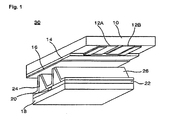
- FIG. 1 is a perspective view illustrating the structure of a conventional plasma display panel.
- the plasma display panel includes a scan electrode 12A and a sustain electrode 12B formed on an upper substrate 10, and an address electrode 20 formed on a lower substrate 18.
- the scan electrode 12A and the sustain electrode 12B each include a transparent electrode and a bus electrode.
- the transparent electrode is made of Indium-Tin-Oxide (ITO).
- the bus electrode is made of a metal to reduce resistance.
- An upper dielectric layer 14 and a protection layer 16 are laminated onto the upper substrate 10 on which the scan electrode 12A and the sustain electrode 12B are formed.
- the protection layer 16 prevents a damage of the upper dielectric layer 14 by sputtering generated by discharge of the plasma, and also enhances emission efficiency of secondary electrons.
- the protection layer 16 is generally formed of magnesium oxide (MgO).
- a lower dielectric layer 22 and a barrier rib 24 are formed on a lower substrate 18 on which the address electrode 20 is formed. Surfaces of the lower dielectric layer 22 and the barrier rib 24 are coated with a phosphor layer 26.
- the address electrode 20 is formed in a direction such that the scan electrode 12A and the sustain electrode 12B are crossed
- the separator 24 is formed with parallel to the address electrode 20, thereby preventing an ultraviolet ray and a visible ray generated by discharging from leaking to adjacent discharge cells.
- the phosphor layer 26 is excited by the ultraviolet ray generated by discharge of the plasma, thereby generating at least one visible ray from red, green or blue.
- An inert gas mixture such as He+Xe, Ne+Xe and others is injected into a discharge space of a discharge cell provided between the upper/lower substrates 10, 18 and the barrier rib 24.
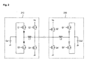
- FIG. 2 shows a recovery circuit of energy of a prior plasma display apparatus
- FIG. 3 shows the waveform of a sustain pulse in operation of a conventional energy recovery circuit.
- the conventional energy recovery circuit is mainly operated in four steps.
- a first switch Q1 for a scan electrode and a fourth switch Q4' for a sustain electrode contained in a energy recovery circuit 210 for a scan electrode are turned on, and a second to a fourth switches Q2, Q3, Q4 for a scan electrode and a first to a third switches Q1', Q2', Q3' for a sustain electrode are turned off.
- an energy stored in a capacitor Cs1 is supplied to a panel Cp by means of resonance of a coil L1, thereby causing a voltage (hereinafter, referred to as V PY ) to be increased in the scan electrode.
- a second switch S2 for a scan electrode is turned on, and a fourth switch Q4' for a sustain electrode is kept in the turned-on state, and a first switch Q1 for a scan electrode, a third switch Q3 for a scan electrode and a fourth switch Q4 for a scan electrode are turned off.
- the V PY is sustained at the sustain voltage Vs.
- a third switch Q3 for a scan electrode is turned on, and a fourth switch Q4' for a sustain electrode is kept in the turned-on state, and a first switch Q 1 for a scan electrode, a third switch Q3 for a scan electrode and a fourth switch Q4 for a scan electrode are turned off.
- a fourth switch Q4 for a scan electrode is turned on, and a fourth switch Q4' for a sustain electrode is kept in the turned-on state, and a first switch Q1 for a scan electrode, a second switch Q2 for a scan electrode and a third switch Q3 for a scan electrode are turned off.
- the V PY drops to ground level.
- the sustain pulse is applied to the scan electrode by means of such a process.
- the operation order of the first to the fourth switch Q1'-Q4' for a sustain electrode is identical to the above-described operation order of the first to the fourth switch Q1-Q4 for a sustain electrode.
- an object of embodiments of the present invention is to solve at least the problems and disadvantages of the background art.
- a plasma display apparatus includes a display panel, a frame disposed at a rear of the display panel, and at least two thermal conductive sheets formed on a side between the display panel and the frame, wherein the thermal conductive sheets separated apart at a predetermined interval.
- the plasma display apparatus includes a plasma display apparatus including a plasma display panel including a scan electrode and a sustain electrode; a first energy supply unit for supplying a first energy corresponding to a first voltage by means of resonance and supplying a first sustain voltage, followed by recovering the first energy by means of resonance; a second energy supply unit for supplying a second energy corresponding to a second voltage having an opposite polarity to the first voltage by means of resonance and supplying a second sustain voltage having an opposite polarity to the first sustain voltage, followed by recovering the second energy by means of resonance; and a path forming unit which serves to supply the first energy to the scan electrode and supply the second energy to the sustain electrode; serves to supply the first sustain voltage to the scan electrode and simultaneously supply the second sustain voltage to the sustain electrode; serves to supply the
- the first energy supply unit supplies or recovers energy corresponding to the first voltage as much as 0.5 times of the first sustain voltage.
- the second energy supply unit supplies or recovers energy corresponding to the second voltage as much as 0.5 times of the second sustain voltage.
- the first energy supply unit supplies the first sustain voltage as much as 0.5 times of the sustain voltage
- the second energy supply unit supplies the second sustain voltage as much as 0.5 times of the negative sustain voltage
- the first energy supply unit includes a) a first supply recovery unit including an energy storing unit for storing energy corresponding to a first voltage; a first switch for forming a path to supply energy corresponding to the first voltage; a second switch for forming a path to recover energy corresponding to the first voltage; and a first inductor for supplying or recovering energy corresponding to the first voltage by means of resonance, and b) a first voltage applying unit including a third switch for applying the first sustain voltage and a fourth switch for recovering energy corresponding to the first voltage, followed by applying a ground level of a voltage.
- a first supply recovery unit including an energy storing unit for storing energy corresponding to a first voltage; a first switch for forming a path to supply energy corresponding to the first voltage; a second switch for forming a path to recover energy corresponding to the first voltage; and a first inductor for supplying or recovering energy corresponding to the first voltage by means of resonance
- a first voltage applying unit including a third switch for applying the first sustain voltage and
- the second energy supply unit includes a) a second supply recovery unit including an energy storing unit for storing energy corresponding to the second voltage; the twelfth switch for forming a path to supply energy corresponding to the second voltage; an eleventh switch for forming a path to recover energy corresponding to the second voltage; and a second inductor for supplying or recovering energy corresponding to the second voltage by means of resonance, and b) a second voltage applying unit including a tenth switch for applying the second sustain voltage and a ninth switch for recovering energy corresponding to the second voltage, followed by applying a ground level of a voltage.
- a second supply recovery unit including an energy storing unit for storing energy corresponding to the second voltage; the twelfth switch for forming a path to supply energy corresponding to the second voltage; an eleventh switch for forming a path to recover energy corresponding to the second voltage; and a second inductor for supplying or recovering energy corresponding to the second voltage by means of resonance
- a second voltage applying unit including a tenth
- the path forming unit includes a) a fifth switch for supplying or recovering the first energy to the scan electrode and applying the first sustain voltage or the ground level of the voltage to the scan electrode; b) an eighth switch for supplying or recovering the second energy to the sustain electrode and applying the second sustain voltage or the ground level of the voltage to the sustain electrode; c) a seventh switch for supplying or recovering the first energy to the sustain electrode and applying the first sustain voltage or the ground level of the voltage to the sustain electrode; and d) a sixth switch for supplying or recovering the second energy to the scan electrode and applying the second sustain voltage or the level of the voltage to the scan electrode.
- the fifth switch has one end connected with the scan electrode and the other end connected with the first energy supply unit; the eighth switch has one end connected with the sustain electrode and the other end connected with the second energy supply unit; the seventh switch has one end connected with the sustain electrode and the other end connected with the other end of the fifth switch; and the sixth switch has one end connected with the scan electrode and the other end connected with the other end of the eighth switch.
- a plasma display apparatus includes a plasma display panel including a scan electrode and a sustain electrode; a first energy supply unit for supplying a first energy corresponding to a first voltage by means of resonance, and supplying a first sustain voltage, followed by recovering the first energy by means of resonance; a second energy supply unit for supplying a second energy corresponding to a second voltage having an opposite polarity to the first voltage by means of resonance, and supplying a second sustain voltage having an opposite polarity to the first sustain voltage, followed by recovering the second energy by means of resonance; a first voltage sustain unit for applying the first sustain voltage or a ground level of a voltage; a second voltage sustain unit for applying the second sustain voltage or a ground level of a voltage; and a path forming unit which serves to supply the first energy to the scan electrode and supply the second energy to the sustain electrode; serves to supply the first sustain voltage from at least one of the first energy supply unit and the first voltage sustain unit to the scan electrode and simultaneously supply the second sustain voltage from at least one of the second energy supply unit and the second voltage sustain unit
- the first energy supply unit supplies or recovers energy corresponding to the first voltage as much as 0.5 times of the first sustain voltage.
- the second energy supply unit supplies or recovers energy corresponding to the second voltage as much as 0.5 times of the second sustain voltage.
- the first energy supply unit and the first voltage sustain unit supplies the first sustain voltage as much as 0.5 times of the sustain voltage
- the second energy supply unit and the second voltage sustain unit supplies the second sustain voltage as much as 0.5 times of the negative sustain voltage.
- the path forming unit includes a) a fifth switch for supplying or recovering the first energy to the scan electrode and applying the first sustain voltage or a ground level of a voltage to the scan electrode; b) a eighth switch for supplying or recovering the second energy to the sustain electrode and applying the second sustain voltage or a ground level of a voltage to the sustain electrode; c) a seventh switch for supplying or recovering the first energy to the a sustain electrode and applying the first sustain voltage or a ground level of a voltage to the sustain electrode; and d) a sixth switch for supplying or recovering the second energy to the scan electrode and applying the second sustain voltage or a ground level of a voltage to the scan electrode.
- the fifth switch has one end connected with the scan electrode and the other end connected together with the first energy supply unit and the first voltage sustain unit;
- the eighth switch has one end connected with the sustain electrode and the other end connected together with the second energy supply unit and the second voltage sustain unit;
- the seventh switch has one end connected with the sustain electrode and the other end connected together with the other end of the fifth switch and the first voltage sustain unit;
- the sixth switch has one end connected with the scan electrode and the other end connected together with the other end of the eighth switch and the second voltage sustain unit.
- the first voltage sustain unit includes a sixteenth switch M 16 for forming a path to apply the first sustain voltage, and a fifteenth switch M15 for forming a path to apply a ground level of a voltage.
- the second voltage sustain unit includes a thirteenth switch for forming a path to supply the first sustain voltage V1, and a fourteenth switch for forming a path to supply a ground level of a voltage.
- a method for driving a plasma display apparatus includes forming a path to supply the first energy to the scan electrode and forming a path to supply the second energy to the sustain electrode; forming a path to supply the first sustain voltage to the scan electrode and forming a path to supply the second sustain voltage to the sustain electrode; forming a path to recover the first energy from the scan electrode and recover the second energy from the sustain electrode; forming a path to supply a ground level of a voltage to the scan electrode and supply a ground level of a voltage to the sustain electrode; forming a path to supply the first energy to the sustain electrode and supply the second energy to the scan electrode; forming a path to supply the first sustain voltage to the sustain electrode and supply the second sustain voltage to the scan electrode; forming a path to recover the first energy from the sustain electrode and recover the second energy from the scan electrode; and forming a path to supply a ground level of a voltage to the sustain electrode and supply a ground level of a voltage to the scan electrode.
- the first voltage is 0.5 times of the first sustain voltage.
- the voltage is 0.5 times of the second sustain voltage.
- the first sustain voltage is 0.5 times of the positive sustain voltage
- the second sustain voltage is 0.5 times of the negative sustain voltage
- FIG. 1 is a perspective view illustrating the structure of a conventional plasma display panel.
- FIG. 2 shows a conventional energy recovery circuit for a plasma display apparatus.
- FIG. 3 shows the waveform of a sustain pulse in the conventional energy recovery circuit.
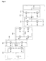
- FIG. 4 shows a circuit diagram of a first embodiment of a plasma display apparatus.
- FIG. 5 shows a waveform view in accordance with operation of the plasma display apparatus of the first embodiment.
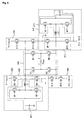
- FIG. 6 shows a circuit diagram of a second embodiment of a plasma display apparatus.
- FIG. 7 shows a waveform view in accordance with operation of the plasma display apparatus of the second embodiment.
- a first plasma display apparatus includes a plasma display panel, a first energy supply unit 400, a second energy supply unit 410 and a path forming unit 420.
- the plasma display panel includes a scan electrode Y and a sustain electrode Z.
- the first energy supply unit 400 supplies a first energy corresponding to the first voltage by means of resonance, supplies a first sustain voltage V1, and then recovers the first energy by means of resonance.
- the first voltage preferably corresponds to 0.5 times of the first sustain voltage V1
- the first sustain voltage V1 preferably corresponds to 0.5 times of the sustain voltage Vs which generates a sustain discharge.
- the first energy supply unit 400 includes a supply recovery unit 401 and a first voltage applying unit 403.
- the first supply recovery unit 401 includes a energy storing unit C 1 for storing energy corresponding to the first voltage, a first switch M1 for forming a path to supply energy corresponding to the first voltage, a second switch M2 for forming a path to recover energy corresponding to the first voltage, and a first inductor L 1 for supplying or recovering energy corresponding to the first voltage by means of resonance.
- the first voltage applying unit 403 includes a third switch M3 for applying a first sustain voltage V1 and a fourth switch M4 for recovering energy corresponding to the first voltage, followed by applying a ground level of a voltage.
- the second energy supply unit 410 supplies a second energy corresponding to a second voltage having an opposite polarity to the first voltage by means of resonance, supplies a second sustain voltage V2 having an opposite polarity to the first sustain voltage V1, and then recovers the second energy by means of resonance.
- the second voltage preferably corresponds to 0.5 times of the second sustain voltage V2
- the second sustain voltage V2 preferably corresponds to 0.5 times of the negative sustain voltage -Vs which generates a sustain discharge.
- the second energy supply unit 410 includes a second supply recovery unit 411 and a second voltage applying unit 413.
- the second supply recovery unit 411 includes a energy storing unit C2 for storing energy corresponding to the second voltage, a mixture switch M12 for forming a path to supply energy corresponding to the second voltage, a eleventh switch M11 for forming a path to recover energy corresponding to the second voltage, and a second inductor L2 for supplying or recovering energy corresponding to the second voltage by means of resonance.
- the second voltage applying unit 413 includes a tenth switch M10 for applying the second sustain voltage V2 and a ninth switch M9 for recovering energy corresponding to the second voltage, followed by applying a ground level of a voltage.
- the path forming unit 420 serves to supply the first energy to the scan electrode Y and supply the second energy to the sustain electrode Z; serves to supply the first sustain voltage V1 to the scan electrode Y and supply the second sustain voltage V2 to the sustain electrode Z; serves to supply the first energy to the sustain electrode Z and supply the second energy to the scan electrode Y; and also serves to supply the first sustain voltage V1 to the sustain electrode Z and supply the second sustain voltage V2 to the scan electrode Y.
- Such a path forming unit 420 is shown as an "H- switch" or bridge circuit of four FETs M5-M8., with the panel forming a diagonal.
- the bridge includes a fifth switch M5 for supplying or recovering the first energy to/from the scan electrode Y and applying the first sustain voltage V 1 or a ground level of a voltage to the scan electrode Y; a eighth switch M8 for supplying or recovering the second energy to/from the sustain electrode Z and applying the second sustain voltage V2 or a ground level of a voltage to the sustain electrode Z; a seventh switch M7 for supplying or recovering the first energy to/from the sustain electrode Z and applying the first sustain voltage V1 or a ground level of a voltage to the sustain electrode Z, and a sixth switch M6 for supplying or recovering the second energy to/from the scan electrode Y and applying the second sustain voltage V2 or a ground level of a voltage to the scan electrode Y.
- the above fifth switch M5 has one end connected with the scan electrode Y and the other end connected with the first energy supply unit 400.
- the eighth switch M8 has one end connected with the sustain electrode Z and the other end connected with the second energy supply member 410.
- the seventh switch M7 has one end connected with the sustain electrode Z and the other end connected with the other end of the fifth switch M5.
- the sixth switch M6 has one end connected with the scan electrode Y and the other end connected with the other end of the eighth switch M8.
- a first step S1 the first switch M 1 of the first energy supply unit 400 and the fifth switch M5 of the path forming unit 420 are turned on, and the twelfth switch M12 of the second energy supply unit 410 and the eighth switch M8 of the path forming unit 420 are turned off. Therefore, the first energy and the second energy each stored in the first energy storing unit C 1 and the second energy storing unit C2 are supplied to a scan electrode Y and a sustain electrode Z by means of resonance with the first inductor L 1 and the second inductor L2, respectively. Therefore, a voltage of the scan electrode Y is increased to Vs/2, and a voltage of the sustain electrode Z is reduced to - Vs/2.
- the third switch M3 of the first energy supply unit 400 and the fifth switch M5 of the path forming unit 420 are turned on, and the tenth switch M10 of the second energy supply unit 410 and the eighth switch M8 of the path forming unit 420 are turned off. Therefore, a voltage of the scan electrode Y is sustained at a range of Vs/2, and a voltage of the sustain electrode Z is sustained at a range of-Vs/2.
- the second switch M2 of the first energy supply unit 400 and the fifth switch M5 of the path forming unit 420 are turned on, and the eleventh switch M11 of the second energy supply unit 410 and the eighth switch M8 of the path forming unit 420 are turned off.
- the first energy and the second energy are recovered from the scan electrode Y and the sustain electrode Z to the first energy storing unit C 1 and the second energy storing unit C2 by means of resonance with the first inductor L 1 and the second inductor L2, respectively. Therefore, voltages of the scan electrode Y and the sustain electrode Z are dropped to a ground level.
- the fourth switch M4 of the first energy supply unit 400 and the fifth switch M5 of a path forming unit 420 are turn on, and the ninth switch M9 of the second energy supply unit 410 and the eighth switch M8 of the path forming unit 420 are turn on. Therefore, a voltage of a scan electrode Y and a sustain electrode Z is sustained to ground level.
- the first switch M 1 of the first energy supply unit 400 and the seventh switch M7 of the path forming unit 420 are turned on, and the twelfth switch M12 of the second energy supply unit 410 and the sixth switch M6 of the path forming unit 420 are turned off. Therefore, the first energy and the second energy each stored in the first energy storing unit C1 and the second energy storing unit C2 are supplied to the sustain electrode Z and the scan electrode Y by means of resonance with the first inductor L1 and the second inductor L2, respectively. Therefore, a voltage of the scan electrode Y is dropped to -Vs/2, and a voltage of the sustain electrode Z is increased to Vs/2.
- the third switch M3 of the first energy supply unit 400 and the seventh switch M7 of the path forming unit 420 are turned on, and the tenth switch M 10 of the second energy supply unit 410 and the eighth switch M8 of the path forming unit 420 are turned on. Therefore, a voltage of the scan electrode Y is sustained at a range of-Vs/2, and a voltage of the sustain electrode Z is sustained at a range of Vs/2.
- the second switch M2 of the first energy supply unit 400 and the seventh switch M7 of the path forming unit 420 are turned on, and the eleventh switch M11 of the second energy supply unit 410 and the sixth switch M6 of the path forming unit 420 are turned on.
- the first energy and the second energy are recovered from the sustain electrode Z and the scan electrode Y to the first energy storing unit C 1 and the second energy storing unit C2 by means of resonance with the first inductor L1 and the second inductor L2, respectively. Therefore, voltages of the scan electrode Y and the sustain electrode Z are dropped to a ground level.
- the fourth switch M4 of the first energy supply unit 400 and the seventh switch M7 of the path forming unit 420 are turned on, and the ninth switch M9 of the second energy supply unit 410 and the sixth switch M6 of the path forming unit 420 are turned on. Therefore, voltages of the scan electrode Y and the sustain electrode Z are sustained at a ground level.
- a second plasma display apparatus includes a plasma display panel, a first energy supply unit 400, a second energy supply unit 410, a first voltage sustain unit 430, a second voltage sustain unit 440 and a path forming unit 420.
- the plasma display panel includes a scan electrode Y and a sustain electrode Z.
- the first energy supply unit 400 supplies a first energy corresponding to the first voltage by means of resonance and supplies a first sustain voltage V1, and then recovers the first energy by means of resonance.
- the first voltage preferably corresponds to 0.5 times of the first sustain voltage V1
- the first sustain voltage V1 preferably corresponds to 0.5 times of a sustain voltage Vs which generates a sustain discharge.
- Such a first energy supply unit 400 includes a first supply recovery unit 401 and a first voltage applying unit 403.
- the first supply recovery unit 401 includes an energy storing unit C for storing energy corresponding to the first voltage, a first switch M 1 for forming a path to supply energy corresponding to the first voltage, a second switch M2 for forming a path to recover energy corresponding to the first voltage, and a first inductor L1 for supplying or recovering energy corresponding to the first voltage by means of resonance.
- the first voltage applying unit 403 includes a third switch M3 for applying the first sustain voltage V1 and a fourth switch M4 for recovering energy corresponding to the first voltage, followed by applying a ground level of a voltage.
- the second energy supply unit 410 supplies a second energy corresponding to the second voltage having an opposite polarity to the first voltage by means of resonance, supplies the second sustain voltage V2 having an opposite polarity to the first sustain voltage V1, and then recovers the second energy by means of resonance.
- the second voltage preferably corresponds to 0.5 times of the second sustain voltage V2
- the second sustain voltage V2 preferably corresponds to 0.5 times of the negative sustain voltage -Vs which generates a sustain discharge.
- the second energy supply unit 400 includes a second supply recovery unit 401 and a second voltage applying unit 403.
- the second supply recovery unit 401 includes an energy storing unit C2 for storing energy corresponding to the second voltage, a twelfth switch M12 for forming a path to supply energy corresponding to the second voltage, a eleventh switch M11 for forming a path to recover energy corresponding to the second voltage, and a second inductor L2 for supplying or recovering energy corresponding to the second voltage by means of resonance.
- the second voltage applying unit 413 includes a tenth switch M10 for applying the second sustain voltage V2 and a ninth switch M9 for recovering energy corresponding to the second voltage, followed by applying a ground level of a voltage.
- the first voltage sustain unit 430 applies the first sustain voltage V1 or a ground level of a voltage.
- the first voltage sustain unit 430 includes a fifteenth switch M15 and a sixteenth switch M16.
- the sixteenth switch M16 forms a path to apply the first sustain voltage V1
- the fifteenth switch M15 forms a path to apply a ground level of voltage.
- the fifteenth switch M15 and the sixteenth switch M16 are connected in series to each other.
- the second voltage sustain unit 440 applies the second sustain voltage V2 or a ground level of a voltage.
- the second voltage sustain unit 440 includes a thirteenth switch M13 and a fourteenth switch M 4.
- the thirteenth switch M13 forms a path to apply the first sustain voltage V1
- the fourteenth switch M14 forms a path to apply a ground level of a voltage.
- the thirteenth switch M 13 and the fourteenth switch M 14 are connected in series to each other.
- the path forming unit 420 serves to supply the first energy to the scan electrode Y and supply the second energy the sustain electrode Z; serves to supply the first sustain voltage V1 from at least one of the first voltage applying unit 403 of the first energy supply unit 400 and the first voltage sustain unit 430 to the scan electrode Y and supply the second sustain voltage V2 from at least one of the second voltage applying unit 413 of the second energy supply unit 410 and the second voltage sustain unit 440 to the sustain electrode Z; serves to supply the first energy to the sustain electrode Z and supply the second energy to the scan electrode Y; and also serves to supply the first sustain voltage V1 from at least one of the first supply recovery unit 401 of the first energy supply unit 400 and the first voltage sustain unit 430 to the sustain electrode Z and supply the second sustain voltage V2 from at least one of the second voltage applying unit 413 of the second energy supply unit 410 and the second voltage sustain unit 440 to the scan electrode Y.
- the above path forming unit 420 includes a fifth switch M5 for supplying or recovering the first energy to/from the scan electrode Y and applying the first sustain voltage V1 or a ground level of a voltage to the scan electrode Y; a eighth switch M8 for supplying or recovering the second energy to/from the sustain electrode Z and applying the second sustain voltage V2 or a ground level of a voltage to the sustain electrode Z; a seventh switch M7 for supplying or recovering the first energy to/from the sustain electrode Z and applying the first sustain voltage V1 or a ground level of a voltage to the sustain electrode Z; and a sixth switch M6 for supplying or recovering the second energy to/from the scan electrode Y and applying the second sustain voltage V2 or a ground level of a voltage to the scan electrode Y.
- the fifth switch M5 has one end connected with the scan electrode Y and the other end connected with the first energy supply unit 400.
- the eighth switch M8 has one end connected with the sustain electrode Z and the other end connected with the second energy supply unit 410.
- the seventh switch M7 has one end connected with the sustain electrode Z and the other end connected with the other end of the fifth switch M5.
- the sixth switch M6 has one end connected with the scan electrode Y and the other end connected with the other end of the eighth switch M8.
- a first step S1 the first switch M1 of the first energy supply unit 400 and the fifth switch M5 of the path forming unit 420 are turned on, and the twelfth switch M12 of the second energy supply unit 410 and the eighth switch M8 of the path forming unit 420 are turned on. Therefore, the first energy and the second energy each stored in the first energy storing unit C1 and the second energy storing unit C2 are supplied to the scan electrode Y and the sustain electrode Z by means of resonance with the first inductor L and the second inductor L2, respectively. Therefore, a voltage of the scan electrode Y is increased to Vs/2, and a voltage of the sustain electrode Z is dropped to -Vs/2.
- the second step S2 at least one of the third switch M3 of the first energy supply unit 400 and the sixteenth switch M16 of the first voltage sustain unit 430, and the fifth switch M5 of the path forming unit 420 are turned on, and at least one of the tenth switch M10 of the second energy supply unit 410 and the thirteenth switch M13 of the second voltage sustain unit, and the eighth switch M8 of the path forming unit 420 are turned on. Therefore, a voltage of the scan electrode Y is sustained at a range of Vs/2, and a voltage of the sustain electrode Z is sustained at a range of -Vs/2.
- the second switch M2 of the first energy supply unit 400 and the fifth switch M5 of the path forming unit 420 are turned on, and the eleventh switch M11 of the second energy supply unit 410 and the eighth switch M8 of the path forming unit 420 are turned on.
- the first energy and the second energy are recovered from the scan electrode Y and the sustain electrode Z to the first energy storing unit C 1 and the second energy storing unit C2 by means of resonance with the first inductor L 1 and the second inductor L2, respectively. Therefore, voltages of the scan electrode Y and the sustain electrode Z are dropped to a ground level.
- step S4 at least one of the fourth switch M4 of the first energy supply unit 400 and the fifteenth switch M 15 of the first voltage sustain unit, and the fifth switch M5 of the path forming unit 420 are turned on, and at least one of the ninth switch M9 of the second energy supply unit 410 and the fourteenth switch M 14 of the second voltage sustain unit 440, and the eighth switch M8 of the path forming unit 420 are turned on. Therefore, voltages of the scan electrode Y and the sustain electrode Z are sustained at a ground level.
- the first switch M of the first energy supply unit 400 and the seventh switch M7 of the path forming unit 420 are turned on, and the twelfth switch M12 of the second energy supply unit 410 and the sixth switch M6 of the path forming unit 420 are turned on. Therefore, the first energy and the second energy each stored in the first energy storing unit C 1 and the second energy storing unit C2 are supplied to the sustain electrode Z and the scan electrode Y by means of resonance with the first inductor L1 and the second inductor L2, respectively. Therefore, a voltage of the scan electrode Y is dropped to -Vs/2, and a voltage of the sustain electrode Z is increased to Vs/2.
- step S6 at least one of the third switch M3 of the first energy supply unit 400 and the sixteenth switch M16 of the first voltage sustain unit 430, and the seventh switch M7 of the path forming unit 420 are turned on, and at least one of the tenth switch M10 of the second energy supply unit 410 and the thirteenth switch M13 of the second voltage sustain unit 440, and the eighth switch M8 of the path forming unit 420 are turned on. Therefore, a voltage of the scan electrode Y is sustained at a range of-Vs/2, and a voltage of the sustain electrode Z is sustained at a range of Vs/2.
- the second switch M2 of the first energy supply unit 400 and the seventh switch M7 of the path forming unit 420 are turned on, and the eleventh switch M11 of the second energy supply unit 410 and the sixth switch M6 of the path forming unit 420 are turned on.
- the first energy and the second energy are recovered from the sustain electrode Z and the scan electrode Y to the first energy storing unit C1 and the second energy storing unit C2 by means of resonance with the first inductor L1 and the second inductor L2, respectively. Therefore, a voltage of a scan electrode Y and a sustain electrode Z drop to ground level.
- step S8 at least one of the fourth switch M4 of the first energy supply unit 400 and the fifteenth switch M15 of the first voltage sustain unit 430, and the seventh switch M7 of the path forming unit 420 are turned on, and at least one of the ninth switch M9 of the second energy supply unit 410 and the fourteenth switch M14 of the second voltage sustain unit 440, and the sixth switch M6 of the path forming unit 420 are turned on. Therefore, voltages of the scan electrode Y and the sustain electrode Z are sustained at a ground level.
- the second embodiment is different from the first embodiment in that it further includes the first voltage sustain unit 430 and the second voltage sustain unit 440 so that it can conduct a more reliable voltage sustain operation than when specific voltages are sustained in the scan electrode Y or the sustain electrode Z.
Landscapes
- Engineering & Computer Science (AREA)
- Power Engineering (AREA)
- Physics & Mathematics (AREA)
- Plasma & Fusion (AREA)
- Computer Hardware Design (AREA)
- General Physics & Mathematics (AREA)
- Theoretical Computer Science (AREA)
- Control Of Indicators Other Than Cathode Ray Tubes (AREA)
- Control Of Gas Discharge Display Tubes (AREA)
Applications Claiming Priority (2)
| Application Number | Priority Date | Filing Date | Title |
|---|---|---|---|
| KR1020040071461A KR100625582B1 (ko) | 2004-09-07 | 2004-09-07 | 플라즈마 표시 패널의 구동 장치 |
| KR1020040071462A KR101051990B1 (ko) | 2004-09-07 | 2004-09-07 | 플라즈마 표시 패널의 구동 회로 |
Publications (2)
| Publication Number | Publication Date |
|---|---|
| EP1632928A2 true EP1632928A2 (de) | 2006-03-08 |
| EP1632928A3 EP1632928A3 (de) | 2006-10-11 |
Family
ID=36158549
Family Applications (1)
| Application Number | Title | Priority Date | Filing Date |
|---|---|---|---|
| EP05255467A Withdrawn EP1632928A3 (de) | 2004-09-07 | 2005-09-07 | Vorrrichtung und Verfahren zur Energierückgewinnung für ein Plasmadisplay |
Country Status (3)
| Country | Link |
|---|---|
| US (1) | US20060050067A1 (de) |
| EP (1) | EP1632928A3 (de) |
| JP (1) | JP4699146B2 (de) |
Families Citing this family (2)
| Publication number | Priority date | Publication date | Assignee | Title |
|---|---|---|---|---|
| KR100908714B1 (ko) * | 2005-01-17 | 2009-07-22 | 삼성에스디아이 주식회사 | 플라즈마 표시 장치 및 그 구동 방법 |
| CN100418119C (zh) * | 2006-05-24 | 2008-09-10 | 乐金电子(南京)等离子有限公司 | 等离子显示装置 |
Citations (1)
| Publication number | Priority date | Publication date | Assignee | Title |
|---|---|---|---|---|
| US20030085886A1 (en) * | 2001-11-06 | 2003-05-08 | Pioneer Corporation | Display panel driving apparatus having a structure capable of reducing power loss |
Family Cites Families (27)
| Publication number | Priority date | Publication date | Assignee | Title |
|---|---|---|---|---|
| JP2755201B2 (ja) * | 1994-09-28 | 1998-05-20 | 日本電気株式会社 | プラズマディスプレイパネルの駆動回路 |
| KR100222203B1 (ko) * | 1997-03-17 | 1999-10-01 | 구자홍 | AC 플라즈마 디스플레이 패널을 위한 에너지 리커버리(recovery) 서스테인 회로 |
| JP3642693B2 (ja) * | 1998-12-28 | 2005-04-27 | 富士通株式会社 | プラズマディスプレイパネル装置 |
| JP3201603B1 (ja) * | 1999-06-30 | 2001-08-27 | 富士通株式会社 | 駆動装置、駆動方法およびプラズマディスプレイパネルの駆動回路 |
| JP3595273B2 (ja) * | 2000-03-13 | 2004-12-02 | 松下電器産業株式会社 | パネル表示装置 |
| JP2002351388A (ja) * | 2001-05-22 | 2002-12-06 | Fujitsu Hitachi Plasma Display Ltd | プラズマディスプレイ装置 |
| KR100463185B1 (ko) * | 2001-10-15 | 2004-12-23 | 삼성에스디아이 주식회사 | 플라즈마 디스플레이 패널, 그의 구동 장치 및 그의 구동방법 |
| KR100477985B1 (ko) * | 2001-10-29 | 2005-03-23 | 삼성에스디아이 주식회사 | 플라즈마 디스플레이 패널, 그의 구동 장치 및 그의 구동방법 |
| KR100456680B1 (ko) * | 2002-01-11 | 2004-11-10 | 재단법인서울대학교산학협력재단 | 플라즈마 디스플레이 패널의 전력 회수 구동 회로 |
| EP1483756A2 (de) * | 2002-03-06 | 2004-12-08 | Koninklijke Philips Electronics N.V. | Anzeigetafel mit energierückgewinnungssystem |
| JP4160764B2 (ja) * | 2002-03-20 | 2008-10-08 | 株式会社日立製作所 | プラズマディスプレイ装置 |
| JP4299497B2 (ja) * | 2002-05-16 | 2009-07-22 | 日立プラズマディスプレイ株式会社 | 駆動回路 |
| FR2840440B1 (fr) * | 2002-05-31 | 2004-09-10 | Thomson Plasma | Dispositif d'alimentation d'electrodes d'un panneau de visualisation a plasma |
| US6903515B2 (en) * | 2002-06-21 | 2005-06-07 | Lg Electronics Inc. | Sustain driving apparatus and method for plasma display panel |
| KR100458571B1 (ko) * | 2002-07-02 | 2004-12-03 | 삼성에스디아이 주식회사 | 플라즈마 디스플레이 패널의 구동 장치 및 구동 방법 |
| KR100458572B1 (ko) * | 2002-07-09 | 2004-12-03 | 삼성에스디아이 주식회사 | 플라즈마 디스플레이 패널 및 그 구동 방법 |
| JP2004133406A (ja) * | 2002-10-11 | 2004-04-30 | Samsung Sdi Co Ltd | プラズマディスプレイパネルの駆動装置及び駆動方法 |
| KR100467458B1 (ko) * | 2002-10-22 | 2005-01-24 | 삼성에스디아이 주식회사 | 플라즈마 디스플레이 패널의 구동 장치 및 구동 방법 |
| KR100515330B1 (ko) * | 2003-01-29 | 2005-09-15 | 삼성에스디아이 주식회사 | 플라즈마 디스플레이 패널 및 그 구동 장치와 구동 방법 |
| KR100482348B1 (ko) * | 2003-04-16 | 2005-04-14 | 엘지전자 주식회사 | 플라즈마 디스플레이 패널의 에너지 회수장치 및 회수방법 |
| CN1781134A (zh) * | 2003-04-29 | 2006-05-31 | 皇家飞利浦电子股份有限公司 | 等离子体显示面板的能量恢复装置 |
| US7403200B2 (en) * | 2003-05-30 | 2008-07-22 | International Rectifier Corporation | Current sensing bi-directional switch and plasma display driver circuit |
| JP4846974B2 (ja) * | 2003-06-18 | 2011-12-28 | 株式会社日立製作所 | プラズマディスプレイ装置 |
| KR100502931B1 (ko) * | 2003-07-30 | 2005-07-21 | 삼성에스디아이 주식회사 | 플라즈마 디스플레이 패널의 구동 장치와 구동 방법 및플라즈마 표시 장치 |
| KR100503806B1 (ko) * | 2003-08-06 | 2005-07-26 | 삼성전자주식회사 | 환류 전류를 감소시키는 플라즈마 디스플래이 패널서스테인 구동 장치 |
| KR100515334B1 (ko) * | 2003-08-25 | 2005-09-15 | 삼성에스디아이 주식회사 | 플라즈마 디스플레이 패널의 구동장치 및 플라즈마디스플레이 장치 |
| JP2005181890A (ja) * | 2003-12-22 | 2005-07-07 | Fujitsu Hitachi Plasma Display Ltd | 駆動回路及びプラズマディスプレイ装置 |
-
2005
- 2005-09-07 JP JP2005259650A patent/JP4699146B2/ja not_active Expired - Fee Related
- 2005-09-07 US US11/219,859 patent/US20060050067A1/en not_active Abandoned
- 2005-09-07 EP EP05255467A patent/EP1632928A3/de not_active Withdrawn
Patent Citations (1)
| Publication number | Priority date | Publication date | Assignee | Title |
|---|---|---|---|---|
| US20030085886A1 (en) * | 2001-11-06 | 2003-05-08 | Pioneer Corporation | Display panel driving apparatus having a structure capable of reducing power loss |
Also Published As
| Publication number | Publication date |
|---|---|
| US20060050067A1 (en) | 2006-03-09 |
| JP4699146B2 (ja) | 2011-06-08 |
| JP2006079090A (ja) | 2006-03-23 |
| EP1632928A3 (de) | 2006-10-11 |
Similar Documents
| Publication | Publication Date | Title |
|---|---|---|
| US20070109229A1 (en) | Energy recovery circuit and driving method thereof | |
| US20060050021A1 (en) | Plasma display apparatus and driving method thereof | |
| EP1632928A2 (de) | Vorrrichtung und Verfahren zur Energierückgewinnung für ein Plasmadisplay | |
| US7692608B2 (en) | Energy recovery circuit and energy recovering method using the same | |
| KR100811536B1 (ko) | 향상된 효율의 서스테인 구동회로를 포함하는 플라즈마디스플레이 패널의 구동 장치 | |
| US20060176247A1 (en) | Plasma display apparatus and driving method thereof | |
| EP1517288A2 (de) | Einrichtung und Verfahren zur Energierückgewinnung fur eine Plasmaanzeigetafel | |
| CN100470618C (zh) | 等离子显示设备及其驱动方法 | |
| KR100625577B1 (ko) | 플라즈마 디스플레이 패널의 구동장치 | |
| KR100607259B1 (ko) | 플라즈마 디스플레이 패널 구동장치 | |
| US7928931B2 (en) | Plasma display apparatus | |
| KR101051990B1 (ko) | 플라즈마 표시 패널의 구동 회로 | |
| US20070046583A1 (en) | Plasma display apparatus and method of driving the same | |
| US7701146B2 (en) | Plasma display apparatus | |
| US7046217B2 (en) | Energy recovery apparatus for plasma display panel | |
| US20070046582A1 (en) | Plasma display apparatus and method of driving the same | |
| EP1739646A2 (de) | Plasmaanzeigevorrichtung und Verfahren zu ihrer Ansteuerung | |
| KR100552625B1 (ko) | 에너지 회수 회로를 포함하는 플라즈마 표시 패널의 구동장치 | |
| KR100730153B1 (ko) | 디스플레이 패널의 전력회수장치 및 이를 구비하는디스플레이 패널의 구동장치 | |
| US20080042932A1 (en) | Plasma display apparatus and method of driving the same | |
| EP1530190A2 (de) | Verfahren und Einrichtung zum Steuern einer Plasmaanzeigetafel | |
| KR20070120081A (ko) | 향상된 효율의 서스테인 구동회로를 포함하는 플라즈마디스플레이 패널의 구동 장치 | |
| JP2007148406A (ja) | プラズマディスプレイ装置 | |
| KR20080041503A (ko) | 플라즈마 디스플레이 패널의 데이터 구동회로 모듈 | |
| KR20100067272A (ko) | 에너지 회수회로 |
Legal Events
| Date | Code | Title | Description |
|---|---|---|---|
| PUAI | Public reference made under article 153(3) epc to a published international application that has entered the european phase |
Free format text: ORIGINAL CODE: 0009012 |
|
| AK | Designated contracting states |
Kind code of ref document: A2 Designated state(s): AT BE BG CH CY CZ DE DK EE ES FI FR GB GR HU IE IS IT LI LT LU LV MC NL PL PT RO SE SI SK TR |
|
| AX | Request for extension of the european patent |
Extension state: AL BA HR MK YU |
|
| PUAL | Search report despatched |
Free format text: ORIGINAL CODE: 0009013 |
|
| AK | Designated contracting states |
Kind code of ref document: A3 Designated state(s): AT BE BG CH CY CZ DE DK EE ES FI FR GB GR HU IE IS IT LI LT LU LV MC NL PL PT RO SE SI SK TR |
|
| AX | Request for extension of the european patent |
Extension state: AL BA HR MK YU |
|
| 17P | Request for examination filed |
Effective date: 20060908 |
|
| 17Q | First examination report despatched |
Effective date: 20070504 |
|
| AKX | Designation fees paid |
Designated state(s): DE FR GB NL |
|
| STAA | Information on the status of an ep patent application or granted ep patent |
Free format text: STATUS: THE APPLICATION IS DEEMED TO BE WITHDRAWN |
|
| 18D | Application deemed to be withdrawn |
Effective date: 20100401 |