EP1632980B1 - instrument à balayage d'un faisceau de particules - Google Patents
instrument à balayage d'un faisceau de particules Download PDFInfo
- Publication number
- EP1632980B1 EP1632980B1 EP05018964A EP05018964A EP1632980B1 EP 1632980 B1 EP1632980 B1 EP 1632980B1 EP 05018964 A EP05018964 A EP 05018964A EP 05018964 A EP05018964 A EP 05018964A EP 1632980 B1 EP1632980 B1 EP 1632980B1
- Authority
- EP
- European Patent Office
- Prior art keywords
- amplifier
- video signal
- signal
- specimen
- predetermined portion
- Prior art date
- Legal status (The legal status is an assumption and is not a legal conclusion. Google has not performed a legal analysis and makes no representation as to the accuracy of the status listed.)
- Ceased
Links
- 239000002245 particle Substances 0.000 title claims description 14
- 230000005855 radiation Effects 0.000 claims description 31
- 239000003990 capacitor Substances 0.000 claims description 7
- 238000000034 method Methods 0.000 claims description 7
- 230000001419 dependent effect Effects 0.000 claims description 3
- 230000003993 interaction Effects 0.000 claims description 3
- 230000000903 blocking effect Effects 0.000 claims description 2
- 230000015556 catabolic process Effects 0.000 description 6
- 238000011084 recovery Methods 0.000 description 6
- 229910052710 silicon Inorganic materials 0.000 description 5
- 239000010703 silicon Substances 0.000 description 5
- XUIMIQQOPSSXEZ-UHFFFAOYSA-N Silicon Chemical compound [Si] XUIMIQQOPSSXEZ-UHFFFAOYSA-N 0.000 description 4
- 238000010894 electron beam technology Methods 0.000 description 4
- 230000005540 biological transmission Effects 0.000 description 3
- 238000010168 coupling process Methods 0.000 description 3
- 238000005859 coupling reaction Methods 0.000 description 3
- 238000010586 diagram Methods 0.000 description 3
- 230000001934 delay Effects 0.000 description 2
- 125000003821 2-(trimethylsilyl)ethoxymethyl group Chemical group [H]C([H])([H])[Si](C([H])([H])[H])(C([H])([H])[H])C([H])([H])C(OC([H])([H])[*])([H])[H] 0.000 description 1
- 230000002238 attenuated effect Effects 0.000 description 1
- 230000000694 effects Effects 0.000 description 1
- 230000005670 electromagnetic radiation Effects 0.000 description 1
- 238000004626 scanning electron microscopy Methods 0.000 description 1
- 150000003376 silicon Chemical class 0.000 description 1
Images
Classifications
-
- H—ELECTRICITY
- H01—ELECTRIC ELEMENTS
- H01J—ELECTRIC DISCHARGE TUBES OR DISCHARGE LAMPS
- H01J37/00—Discharge tubes with provision for introducing objects or material to be exposed to the discharge, e.g. for the purpose of examination or processing thereof
- H01J37/02—Details
- H01J37/244—Detectors; Associated components or circuits therefor
-
- H—ELECTRICITY
- H01—ELECTRIC ELEMENTS
- H01J—ELECTRIC DISCHARGE TUBES OR DISCHARGE LAMPS
- H01J37/00—Discharge tubes with provision for introducing objects or material to be exposed to the discharge, e.g. for the purpose of examination or processing thereof
- H01J37/26—Electron or ion microscopes; Electron or ion diffraction tubes
- H01J37/261—Details
- H01J37/265—Controlling the tube; circuit arrangements adapted to a particular application not otherwise provided, e.g. bright-field-dark-field illumination
-
- H—ELECTRICITY
- H01—ELECTRIC ELEMENTS
- H01J—ELECTRIC DISCHARGE TUBES OR DISCHARGE LAMPS
- H01J37/00—Discharge tubes with provision for introducing objects or material to be exposed to the discharge, e.g. for the purpose of examination or processing thereof
- H01J37/26—Electron or ion microscopes; Electron or ion diffraction tubes
- H01J37/28—Electron or ion microscopes; Electron or ion diffraction tubes with scanning beams
-
- H—ELECTRICITY
- H01—ELECTRIC ELEMENTS
- H01J—ELECTRIC DISCHARGE TUBES OR DISCHARGE LAMPS
- H01J2237/00—Discharge tubes exposing object to beam, e.g. for analysis treatment, etching, imaging
- H01J2237/04—Means for controlling the discharge
- H01J2237/043—Beam blanking
-
- H—ELECTRICITY
- H01—ELECTRIC ELEMENTS
- H01J—ELECTRIC DISCHARGE TUBES OR DISCHARGE LAMPS
- H01J2237/00—Discharge tubes exposing object to beam, e.g. for analysis treatment, etching, imaging
- H01J2237/15—Means for deflecting or directing discharge
- H01J2237/1501—Beam alignment means or procedures
-
- H—ELECTRICITY
- H01—ELECTRIC ELEMENTS
- H01J—ELECTRIC DISCHARGE TUBES OR DISCHARGE LAMPS
- H01J2237/00—Discharge tubes exposing object to beam, e.g. for analysis treatment, etching, imaging
- H01J2237/248—Components associated with the control of the tube
- H01J2237/2485—Electric or electronic means
- H01J2237/2487—Electric or electronic means using digital signal processors
-
- H—ELECTRICITY
- H01—ELECTRIC ELEMENTS
- H01J—ELECTRIC DISCHARGE TUBES OR DISCHARGE LAMPS
- H01J2237/00—Discharge tubes exposing object to beam, e.g. for analysis treatment, etching, imaging
- H01J2237/26—Electron or ion microscopes
- H01J2237/282—Determination of microscope properties
- H01J2237/2826—Calibration
Definitions
- This invention relates to a scanning particle beam instrument such as a scanning electron microscope (SEM), and to a method of producing a video signal using a scanning particle beam instrument.
- a scanning particle beam instrument such as a scanning electron microscope (SEM)
- SEM scanning electron microscope
- Scanning particle beam instruments are, of course, well known.
- Such an instrument typically includes a scanner, a radiation detector and a DC amplifier, the scanner being operable to scan a beam of charged particles in a predetermined pattern relative to a specimen, the radiation detector being operable to generate a signal representative of an instantaneous intensity of radiation resulting from interaction of the beam and a specimen, and the DC amplifier being operable to amplify the signal generated by the radiation detector to produce a video signal suitable for transmission to a display device to cause an image of a scanned portion of a specimen to be displayed.
- radio frequency includes any particle or electromagnetic radiation that may be emitted by or reflected from a specimen.
- a "video signal” is a varying DC signal variable between a lower signal level that would be represented by a display device as black, and an upper signal level that would be represented by the display device as white. Signal levels between the lower and upper signal levels would be represented by the display device as shades of grey.
- the varying DC signal that forms the video signal may be thought of as consisting of a constant DC signal component and a superimposed varying AC signal component.
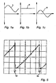
- Figure 1a of the accompanying drawings shows such a varying DC signal (denoted by reference numeral 4) and Figures 1b and 1c show, respectively, the constant DC signal component 6 and varying AC signal component 8 that make up the varying DC signal 4 of Figure 1a .
- the radiation detector of the scanning particle beam instrument is usually subject to a DC offset, such that the signal generated by the detector includes an unwanted DC signal component.
- the signal generated by the detector, including the unwanted DC signal component is amplified by the DC amplifier.
- the DC amplifier is itself usually subject to a DC offset, such that the video signal produced by the DC amplifier includes an unwanted DC signal component made up of the amplified DC offset introduced by the radiation detector, together with the DC offset introduced by the DC amplifier.
- the DC offsets of the detector and DC amplifier are in general subject to drift so that the magnitude of the unwanted DC signal component of the video signal varies over time, the variable unwanted DC signal component of the video signal manifesting itself as regions of varying brightness in images displayed by a display device.
- the regions of varying brightness can be portions of individual lines of the images, entire lines or multiples of entire lines of the images, or even consecutive frames of the images, such that the images appear to flicker.
- a DC signal component to the intermediate signal to obtain the video signal.
- this is done by periodically determining a mean value of the amplified AC signal component, and adding to the amplified AC signal component a DC signal component derived from the mean value of the amplified AC signal component.
- the signal generated by the detector is consistently low or consistently high during the period in which the mean value of the amplified AC signal component is determined, because this causes the mean value of the amplified AC signal component to vary, and hence the DC signal component derived from the mean value of the amplified AC signal component to vary.
- the variable DC signal component of the video signal also manifests itself as regions of varying brightness in images displayed by a display device.
- US3,886,305 discloses a scanning electron microscope in which the contrast and the dark level of the video signal is automatically controlled.
- US 4,099,054 discloses an SEM having a DC bias video signal controlled by maximum and/or minimum of a CRT beam current.
- JP54122971 discloses a scanning electron microscope which can set only the desired part of the scanning picture of CRT to the contrast and luminance suitable for picture pickup.
- the invention therefore provides apparatus that is operable to produce a video signal that is substantially unaffected by any DC offset of the radiation detector or the DC amplifier, or by any drift of any such DC offset.
- the controller may advantageously be operable to cause the scanner to direct the beam to the predetermined portion of the specimen.
- the controller is operable to determine when the beam is directed to a predetermined portion of a specimen as the scanner scans the beam in the predetermined pattern relative to the specimen, and to compare the actual video signal produced by the DC amplifier with the desired video signal while the beam is directed to the predetermined portion of the specimen.
- the predetermined portion of the specimen is preferably chosen such that the beam is directed to the predetermined portion several times as the scanner scans the beam in the predetermined pattern relative to the specimen.
- the predetermined portion it will be directed to a different region of the predetermined portion, as a result of the scanning of the beam in the predetermined pattern.
- the scanner scans the beam in the predetermined pattern relative to the specimen relatively slowly, and may take as long as two minutes to complete the predetermined pattern. Even at rather faster scanning speeds than this, there is nevertheless plenty of time for the controller to compare the actual and desired video signals and to adjust the DC offset of the DC amplifier while the beam is directed to the predetermined portion of the specimen, without any need to cause the beam to dwell on the predetermined portion.
- the DC offset of the detector is dependent on the signal produced by the detector. This is the case, for example, where a reverse-biased silicon diode is used as the detector with a large beam current.
- the DC amplifier could be caused to produce the actual video signal approximating to mid-grey by integrating the signal generated by the detector between operations of the controller to determine the average of the signal generated by the detector (which, in general, will be mid-grey) and operating the controller to apply the average of the signal to the DC amplifier and to compare the actual video signal produced by the amplifier with the desired video signal of that which is represented by the display device as mid-grey.
- the DC amplifier is caused to produce the actual video signal approximating to mid-grey by directing the beam to a predetermined portion of the specimen, as described above, which predetermined portion of the specimen it is known, or it is desired, to be represented by the display device as mid-grey.
- the controller may advantageously be operable to compare the actual video signal produced by the DC amplifier with the desired video signal and to adjust the DC offset of the DC amplifier at intervals selectable by a user of the instrument.
- the DC offsets of the detector and the DC amplifier are in general subject to drift, and such operation enables the user of the instrument to cause the controller to adjust the DC offset of the DC amplifier as often as is necessary to counteract changes in the DC offsets of the detector and DC amplifier.
- the scanner comprises scan coils operable to scan the beam in the raster pattern relative to the specimen, and the controller is operable to compare the actual video signal produced by the DC amplifier with the desired video signal during the line and/or field recovery time of the scan coils.
- the DC amplifier may advantageously be capacitor-coupled to the detector.
- the instrument further comprises an AC amplifier operable to amplify an AC signal component and block a DC signal component of the signal generated by the detector, the DC amplifier being operable by means of the DC offset to add a DC signal component to the signal produced by the AC amplifier, so as to produce the actual video signal.
- an AC amplifier operable to amplify an AC signal component and block a DC signal component of the signal generated by the detector, the DC amplifier being operable by means of the DC offset to add a DC signal component to the signal produced by the AC amplifier, so as to produce the actual video signal.
- the invention therefore further provides an instrument that is operable to produce an actual video signal from a signal generated by the detector, which actual video signal is substantially unaffected by previous values of the signal generated by the detector.
- the instrument is a scanning electron microscope (SEM).
- the method may advantageously further comprise the step of amplifying an AC signal component and blocking a DC signal component of the signal representative of the instantaneous intensity of the radiation by means of an AC amplifier, and, by means of the offset of the DC amplifier, adding a DC signal component to the signal produced by the AC amplifier so as to produce the actual video signal.
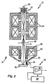
- the scanning electron microscope (SEM) 10 of Figure 2 comprises an electron gun assembly 12 operable to direct a beam 14 of electrons towards a specimen 16, and a radiation detector assembly 18 operable to detect radiation in the form of back-scattered electrons resulting from interaction of the beam 14 and the specimen 16, and to generate a video signal suitable for transmission to a display device to cause an image of a scanned portion of the specimen to be displayed by the display device.
- SEM scanning electron microscope
- the electron gun assembly 12 comprises a heated filament 20, from which electrons are emitted, gun align coils 22, a gun align circuit (not shown in Figure 2 ), condenser lenses 24, objective aperture 26, objective lens 28, a scanner in the form of first and second scan coils 30 and 32, respectively, and a scan generator (not shown in Figure 2 ).
- the gun align coils 22 and gun align circuit direct electrons emitted from the heated filament 20 along the centre of the condenser lenses 24 to the objective aperture 26.
- the condenser lenses 24 focus the electrons passing through them onto the objective aperture 26. Electrons passing through the objective aperture 26 form the beam 14, which is focused onto the specimen 16 by the objective lens 28.
- the first and second scan coils 30 and 32 and scan generator scan the beam of electrons in a raster pattern relative to the specimen 16. As described so far, the operation of the filament 20, gun align coils 22 and circuit, condenser lenses 24, objective lens 28 and scan coils 30 and 32 and generator is identical with the operation of these components in known SEMs.
- the radiation detector assembly 18 comprises a radiation detector in the form of a silicon diode 34, a DC amplifier 36, and a controller in the form of a control circuit 38.
- the silicon diode 34 is reverse-biased in use, and is operable to generate a signal representative of the number of back-scattered electrons resulting from the scanning of the specimen 16 by the beam 14.
- the DC amplifier 36 is operable to amplify the signal generated by the diode 34 to produce a video signal suitable for transmission to a display device (not shown) such as a cathode ray tube.
- the control circuit 38 is operable, during the line and field flyback times of the scan coils 30 and 32 to prevent the beam 14 from reaching the specimen, to compare the actual video signal produced by the DC amplifier 36 with a desired video signal, and to adjust a DC offset of the DC amplifier 36 so as to reduce a difference between the actual video signal produced by the DC amplifier and the desired video signal.
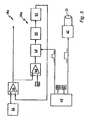
- FIG 3 shows a first example 18a of the radiation detector assembly 18 of Figure 2 , comprising the silicon diode 34, DC amplifier 36 and a first example 38a of the control circuit 38 of Figure 2 .
- the signal generated by the diode 34 is applied to the non-inverting input of the DC amplifier 36.
- the control circuit 38a comprises a desired video signal source 44, a DC amplifier 46, a sample-and-hold circuit 48, an integrator 50 and an attenuator 52, the sample-and-hold circuit 48 being controlled by the scan generator 40.
- the video signal produced by the DC amplifier 36 is applied to the non-inverting input of the DC amplifier 46.
- a desired video signal from the desired video signal source 44 is applied to the inverting input of the DC amplifier 46.
- the desired video signal is that which would be represented by a display device as black.
- the DC amplifier 46 produces an error signal, which it transmits to the sample-and-hold circuit 48.
- the error signal produced by the DC amplifier 46 is disregarded by the sample-and-hold circuit 48.
- the scan generator 40 transmits a first control signal to the gun align circuit 42, which control signal is added to the signal generated by the gun align circuit to control the gun align coils 22.
- the addition of the control signal to the signal generated by the gun align circuit causes the gun align coils to direct the electrons emitted from the filament 20 away from the centre of the condenser lenses 24, such that the electrons do not pass through the objective aperture 26 of the electron gun, and are prevented from reaching the specimen.
- the scan generator 40 delays briefly after transmitting the first control signal to the gun align circuit 42 to allow the first control signal to act to interrupt the electron beam 14.
- the scan generator then transmits a second control signal to the sample-and-hold circuit 48, which samples and holds the error signal produced by the DC amplifier 46 while the electron beam is prevented from reaching the specimen.
- the error signal thus sampled and held is integrated by the integrator 50, attenuated by the attenuator 52 and applied to the inverting input of the DC amplifier 36, so as to reduce the magnitude of the error signal.
- the integrator 50 reduces the impact on an image produced from the video signal of any spurious error signals produced by the DC amplifier 46, which might otherwise give rise to a single scan line of different brightness from the other scan lines making up the image.
- the scan generator again delays briefly to allow for the line scan recovery time of the scan coils 30 and 32, or, if the previous line was the last line of the raster pattern, the field scan recovery time of the scan coils.
- the scan generator then ceases to transmit the first control signal to the gun align circuit, such that the gun align coil again directs the electron beam through the narrow aperture and the electron beam again reaches the specimen; whereupon scanning of the next line of the raster pattern commences.
- This process is repeated whenever the beam reaches the end of a scan line.
- avalanche breakdown of the diode 34 is avoided.
- Avalanche breakdown is only likely to occur when the beam is directed to the specimen and the diode is detecting back-scattered electrons, and can be prevented by ensuring that the beam current does not exceed a threshold level.
- Avoidance of avalanche breakdown of the diode is important because the DC offset of the diode during avalanche breakdown will be very different from the DC offset of the diode during normal conduction, so that the DC offset of the DC amplifier 36, which is set by the control circuit during normal conduction of the diode, will not counteract the DC offset of the diode during avalanche breakdown.
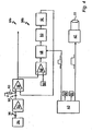
- FIG 4 shows a second example 18b of the radiation detector assembly 18 of Figure 2 , comprising the silicon diode 34, DC amplifier 36 and a second example 38b of the control circuit 38 of Figure 2 .
- the second example 38b of the control circuit differs from the first example 38a in that it includes an AC amplifier 54, an input of which is coupled by a first capacitor 56 to the diode 34, and the output of which is coupled by a second capacitor 58 to the non-inverting input of the DC amplifier 36.
- the other components of the radiation detector assembly are identical with, and operate in the same way as, those of the radiation detector assembly of Figure 3 , and are denoted by the same reference numerals.
- the capacitor-coupling by capacitor 56 of the AC amplifier 54 to the diode 34 blocks the DC signal component of the signal produced by the diode, such that the AC amplifier 54 amplifies only the AC signal component of the signal produced by the diode. Unlike the first example of the radiation detector assembly, therefore, it is unnecessary to avoid avalanche breakdown of the diode 34.
- the AC amplifier 54 itself introduces a DC signal component together with some very low frequency (less than 10Hz, say) signal components into the amplified AC signal.
- the very low frequency AC signal components result from the noise characteristic of the AC amplifier 54.
- the capacitor-coupling by capacitor 58, of the AC amplifier 54 to the DC amplifier 36 again blocks the DC signal component of the amplified AC signal.
- a resistor 60 is connected between the non-inverting input of the DC amplifier 36 and ground. In addition to referencing the non-inverting input of the DC amplifier to ground, the resistor 60 also forms a high-pass filter with the capacitor 58, which serves to attenuate the very low frequency AC signal components of the amplified AC signal produced by the AC amplifier 54.
- Figure 5 this shows two line recovery intervals of the scan coil 30, the line recovery intervals being denoted by reference numerals 62 and 64.
- the time base of the oscillogram of Figure 5 is 0.1ms per division. It can therefore be seen that the time available for the control circuits 38a and 38b to generate the error signal and to adjust the DC offset of the DC amplifier 36 at the end of each line scan is of the order of 20 ⁇ s, which is ample.
- the invention encompasses not only embodiments in which the radiation detector is disposed within a specimen chamber, but also embodiments with a so called in-lens detector, in which the detector is disposed within the electron gun assembly, for example within or shortly above the objective lens.
- an in-lens detector it would preferably be disposed between the objective aperture and the specimen 16, such that electrons that do not pass through the objective aperture cannot reach the detector.
Landscapes
- Chemical & Material Sciences (AREA)
- Analytical Chemistry (AREA)
- Analysing Materials By The Use Of Radiation (AREA)
Claims (8)
- Instrument à balayage d'un faisceau de particules (10) destiné à créer une image d'un échantillon (16) dont une partie prédéterminée doit être représentée par un dispositif d'affichage sous la forme d'un niveau de gris moyen, l'instrument comprenant un dispositif de balayage (30, 32), un détecteur de rayonnement (18) et un amplificateur à courant continu (36), le dispositif de balayage (30, 32) pouvant être mis en fonctionnement pour animer d'un mouvement de balayage un faisceau (14) de particules chargées par rapport à l'échantillon (16), le détecteur de rayonnement (18) ayant pour fonction de générer un signal représentatif d'une intensité de rayonnement résultant de l'interaction entre le faisceau (14) et un échantillon (16), et l'amplificateur à courant continu (36) ayant pour fonction d'amplifier le signal généré par le détecteur de rayonnement (18) afin de produire un signal vidéo, le détecteur étant tel que la sortie du détecteur présente un décalage continu qui dépend du signal produit par le détecteur, l'instrument comprenant également une unité de commande (38), dans lequel l'unité de commande (38) a pour fonction d'interrompre le fonctionnement du dispositif de balayage (30, 32) et de diriger le faisceau (14) vers la partie prédéterminée de l'échantillon (16), ou de déterminer l'instant où le faisceau (14) est dirigé vers la partie prédéterminée de l'échantillon (16) lorsque le dispositif de balayage (30, 32) anime le faisceau (14) d'un mouvement de balayage par rapport à l'échantillon (16), de comparer un signal vidéo effectif produit par l'amplificateur à courant continu (36) à un signal vidéo souhaité pendant que le faisceau (14) est dirigé vers la partie prédéterminée de l'échantillon (16), l'unité de commande (38) ayant pour fonction de faire en sorte que l'amplificateur à courant continu (36) produise un signal vidéo effectif proche d'un niveau de gris moyen en dirigeant le faisceau (14) vers la partie prédéterminée de l'échantillon (16), et de comparer le signal provenant de l'amplificateur à courant continu (36) à un signal vidéo souhaité tel que celui qui est représenté par le dispositif d'affichage sous la forme d'un niveau de gris moyen, et d'ajuster un décalage continu de l'amplificateur à courant continu afin de réduire une différence entre le signal vidéo effectif et le signal vidéo souhaité.
- Instrument selon la revendication 1, dans lequel l'unité de commande (38) a pour fonction de faire en sorte que le dispositif de balayage (30, 32) dirige le faisceau (14) vers la partie prédéterminée de l'échantillon (16).
- Instrument selon la revendication 1 ou la revendication 2, dans lequel l'unité de commande (38) a pour fonction de comparer le signal vidéo effectif produit par l'amplificateur à courant continu (36) au signal vidéo souhaité et d'ajuster le décalage continu de l'amplificateur à courant continu (36) à des intervalles pouvant être sélectionnés par un utilisateur de l'instrument.
- Instrument selon l'une quelconque des revendications précédentes, dans lequel l'amplificateur à courant continu est couplé par condensateur au détecteur de rayonnement.
- Instrument selon l'une quelconque des revendications précédentes, dans lequel l'instrument comprend en outre un amplificateur à courant alternatif ayant pour fonction d'amplifier une composante de signal alternative et d'empêcher le passage d'une composante de signal continue du signal généré par le détecteur, l'amplificateur à courant continu ayant pour fonction, au moyen du décalage continu, d'additionner une composante de signal continue au signal produit par l'amplificateur à courant alternatif, afin de produire le signal vidéo effectif.
- Instrument selon l'une quelconque des revendications précédentes, dans lequel l'instrument est un microscope électronique à balayage (MEB).
- Procédé de production d'un signal vidéo au moyen d'un instrument à balayage d'un faisceau de particules (10) selon l'une quelconque des revendications précédentes, le procédé comprenant les étapes consistant à diriger un faisceau (14) de particules chargées vers un échantillon (16), à animer le faisceau (14) d'un mouvement de balayage par rapport à l'échantillon (16), à détecter un rayonnement émis ou réfléchi par l'échantillon (16) comme résultat du balayage effectué par le faisceau (14) afin de générer un signal représentatif d'une intensité du rayonnement, ledit signal ayant un décalage continu qui dépend du niveau de signal, à amplifier, au moyen d'un amplificateur à courant continu (36), le signal généré par le détecteur de rayonnement afin de produire un signal vidéo effectif, à comparer un signal vidéo effectif produit par l'amplificateur à courant continu (36) à un signal vidéo souhaité, et à ajuster un décalage continu de l'amplificateur à courant continu (36) afin de réduire une différence entre le signal vidéo effectif et le signal vidéo souhaité, dans lequel l'étape de comparaison du signal vidéo effectif au signal vidéo souhaité consiste à diriger le faisceau (14) vers une partie prédéterminée de l'échantillon (16), ou à déterminer l'instant où le faisceau (14) est dirigé vers une partie prédéterminée de l'échantillon (16), et à comparer le signal vidéo effectif au signal vidéo souhaité pendant que le faisceau (14) est dirigé vers la partie prédéterminée de l'échantillon (16), l'étape de comparaison du signal vidéo effectif produit par l'amplificateur à courant continu (36) au signal vidéo souhaité consiste en outre à faire en sorte que l'amplificateur à courant continu (36) produise un signal vidéo effectif proche d'un niveau de gris moyen et à comparer le signal provenant de l'amplificateur à courant continu (36) à un signal vidéo souhaité tel que celui qui est représenté par un dispositif d'affichage sous la forme d'un niveau de gris moyen, et dans lequel l'étape consistant à faire en sorte que l'amplificateur à courant continu (36) produise le signal vidéo effectif proche d'un niveau de gris moyen consiste à diriger le faisceau (14) vers la partie prédéterminée de l'échantillon (16), laquelle partie prédéterminée de l'échantillon (16) doit être représentée par le dispositif d'affichage sous la forme d'un niveau de gris moyen.
- Procédé selon la revendication 7, comprenant en outre l'étape consistant à amplifier une composante de signal alternative et à empêcher le passage d'une composante de signal continue du signal représentatif de l'intensité instantanée du rayonnement au moyen d'un amplificateur à courant alternatif et, au moyen du décalage de l'amplificateur à courant continu, à additionner une composante de signal continue au signal produit par l'amplificateur à courant alternatif afin de produire le signal vidéo effectif.
Applications Claiming Priority (1)
| Application Number | Priority Date | Filing Date | Title |
|---|---|---|---|
| GB0419571A GB2418061B (en) | 2004-09-03 | 2004-09-03 | Scanning particle beam instrument |
Publications (3)
| Publication Number | Publication Date |
|---|---|
| EP1632980A2 EP1632980A2 (fr) | 2006-03-08 |
| EP1632980A3 EP1632980A3 (fr) | 2008-07-23 |
| EP1632980B1 true EP1632980B1 (fr) | 2012-01-18 |
Family
ID=33155971
Family Applications (1)
| Application Number | Title | Priority Date | Filing Date |
|---|---|---|---|
| EP05018964A Ceased EP1632980B1 (fr) | 2004-09-03 | 2005-08-31 | instrument à balayage d'un faisceau de particules |
Country Status (4)
| Country | Link |
|---|---|
| US (1) | US7348557B2 (fr) |
| EP (1) | EP1632980B1 (fr) |
| JP (1) | JP2006073525A (fr) |
| GB (1) | GB2418061B (fr) |
Families Citing this family (31)
| Publication number | Priority date | Publication date | Assignee | Title |
|---|---|---|---|---|
| KR20070038089A (ko) * | 2004-06-03 | 2007-04-09 | 이메이고 사이언티픽 인스트루먼츠 코포레이션 | 레이저 원자 탐침 방법 |
| CN101061759B (zh) | 2004-07-21 | 2011-05-25 | 斯蒂尔瑞弗系统有限公司 | 用于同步回旋加速器的可编程的射频波形发生器 |
| EP1949404B1 (fr) | 2005-11-18 | 2016-06-29 | Mevion Medical Systems, Inc. | Thérapie par rayonnement de particules chargées |
| US8003964B2 (en) | 2007-10-11 | 2011-08-23 | Still River Systems Incorporated | Applying a particle beam to a patient |
| US8581523B2 (en) | 2007-11-30 | 2013-11-12 | Mevion Medical Systems, Inc. | Interrupted particle source |
| US8933650B2 (en) | 2007-11-30 | 2015-01-13 | Mevion Medical Systems, Inc. | Matching a resonant frequency of a resonant cavity to a frequency of an input voltage |
| JP5972677B2 (ja) * | 2012-06-12 | 2016-08-17 | 日本電子株式会社 | 電子顕微鏡の調整方法及び電子顕微鏡 |
| US10254739B2 (en) | 2012-09-28 | 2019-04-09 | Mevion Medical Systems, Inc. | Coil positioning system |
| TWI604868B (zh) | 2012-09-28 | 2017-11-11 | 美威高能離子醫療系統公司 | 粒子加速器及質子治療系統 |
| EP2900326B1 (fr) | 2012-09-28 | 2019-05-01 | Mevion Medical Systems, Inc. | Commande de thérapie par particules |
| WO2014052721A1 (fr) | 2012-09-28 | 2014-04-03 | Mevion Medical Systems, Inc. | Système de commande pour un accélérateur de particules |
| CN104812444B (zh) | 2012-09-28 | 2017-11-21 | 梅维昂医疗系统股份有限公司 | 粒子束的能量调节 |
| CN108770178B (zh) | 2012-09-28 | 2021-04-16 | 迈胜医疗设备有限公司 | 磁场再生器 |
| CN104813750B (zh) | 2012-09-28 | 2018-01-12 | 梅维昂医疗系统股份有限公司 | 调整主线圈位置的磁垫片 |
| CN104813749B (zh) | 2012-09-28 | 2019-07-02 | 梅维昂医疗系统股份有限公司 | 控制粒子束的强度 |
| EP2901822B1 (fr) | 2012-09-28 | 2020-04-08 | Mevion Medical Systems, Inc. | Focalisation d'un faisceau de particules |
| US8791656B1 (en) | 2013-05-31 | 2014-07-29 | Mevion Medical Systems, Inc. | Active return system |
| US9730308B2 (en) | 2013-06-12 | 2017-08-08 | Mevion Medical Systems, Inc. | Particle accelerator that produces charged particles having variable energies |
| US10258810B2 (en) | 2013-09-27 | 2019-04-16 | Mevion Medical Systems, Inc. | Particle beam scanning |
| US9962560B2 (en) | 2013-12-20 | 2018-05-08 | Mevion Medical Systems, Inc. | Collimator and energy degrader |
| US10675487B2 (en) | 2013-12-20 | 2020-06-09 | Mevion Medical Systems, Inc. | Energy degrader enabling high-speed energy switching |
| US9661736B2 (en) | 2014-02-20 | 2017-05-23 | Mevion Medical Systems, Inc. | Scanning system for a particle therapy system |
| US9950194B2 (en) | 2014-09-09 | 2018-04-24 | Mevion Medical Systems, Inc. | Patient positioning system |
| US10786689B2 (en) | 2015-11-10 | 2020-09-29 | Mevion Medical Systems, Inc. | Adaptive aperture |
| EP3481503B1 (fr) | 2016-07-08 | 2021-04-21 | Mevion Medical Systems, Inc. | Planification de traitement |
| US11103730B2 (en) | 2017-02-23 | 2021-08-31 | Mevion Medical Systems, Inc. | Automated treatment in particle therapy |
| JP6940676B2 (ja) | 2017-06-30 | 2021-09-29 | メビオン・メディカル・システムズ・インコーポレーテッド | リニアモーターを使用して制御される構成可能コリメータ |
| JP7311620B2 (ja) | 2019-03-08 | 2023-07-19 | メビオン・メディカル・システムズ・インコーポレーテッド | 粒子線治療システムのためのコリメータおよびエネルギーデグレーダ |
| JP7144485B2 (ja) * | 2020-07-15 | 2022-09-29 | 日本電子株式会社 | 像取得方法および電子顕微鏡 |
| DE102021102900B4 (de) * | 2021-02-08 | 2022-11-17 | Carl Zeiss Microscopy Gmbh | Verfahren zum Betrieb eines Teilchenstrahlgeräts, Computerprogrammprodukt und Teilchenstrahlgerät zur Durchführung des Verfahrens |
| JP7369747B2 (ja) | 2021-09-24 | 2023-10-26 | 日本電子株式会社 | 荷電粒子線装置および画像調整方法 |
Citations (1)
| Publication number | Priority date | Publication date | Assignee | Title |
|---|---|---|---|---|
| JPS54122971A (en) * | 1978-03-16 | 1979-09-22 | Jeol Ltd | Scanning electronic microscope |
Family Cites Families (19)
| Publication number | Priority date | Publication date | Assignee | Title |
|---|---|---|---|---|
| GB1325540A (en) * | 1969-10-10 | 1973-08-01 | Texas Instruments Ltd | Electron beam apparatus |
| US3886305A (en) * | 1972-04-24 | 1975-05-27 | Etec Corp | Automatic contrast and dark level control for scanning electron microscopes |
| JPS5520636B2 (fr) * | 1973-03-27 | 1980-06-04 | ||
| JPS535484Y2 (fr) * | 1973-04-19 | 1978-02-10 | ||
| US4099054A (en) * | 1974-11-20 | 1978-07-04 | Hitachi, Ltd. | Sem having d-c bias of video signal controlled by maximum and/or minimum of crt beam current |
| JPS5160153A (fr) * | 1974-11-20 | 1976-05-25 | Hitachi Ltd | |
| JPS5443458A (en) * | 1977-09-12 | 1979-04-06 | Jeol Ltd | Automatic focusing device of electronic scan microscope |
| US4249244A (en) * | 1978-05-03 | 1981-02-03 | Ppm, Inc. | Electro-optical system and method and apparatus for providing automatically-compensating, traceable calibration and zeroing for light scattering devices |
| US4433247A (en) * | 1981-09-28 | 1984-02-21 | Varian Associates, Inc. | Beam sharing method and apparatus for ion implantation |
| JPS59224038A (ja) * | 1983-06-02 | 1984-12-15 | Shimadzu Corp | 荷電粒子線走査型分析装置 |
| JPS63284746A (ja) * | 1987-05-14 | 1988-11-22 | Nikon Corp | 画像信号処理回路 |
| JPH03269938A (ja) * | 1990-03-19 | 1991-12-02 | Fujitsu Ltd | 走査型電子顕微鏡 |
| JP3170606B2 (ja) * | 1991-08-30 | 2001-05-28 | 光洋精工株式会社 | 一方向クラッチ |
| US5825670A (en) * | 1996-03-04 | 1998-10-20 | Advanced Surface Microscopy | High precison calibration and feature measurement system for a scanning probe microscope |
| JP3346172B2 (ja) * | 1996-06-07 | 2002-11-18 | 株式会社日立製作所 | 走査形顕微鏡 |
| JP2000030652A (ja) * | 1998-07-10 | 2000-01-28 | Hitachi Ltd | 試料の観察方法およびその装置 |
| JP2000101390A (ja) * | 1998-09-18 | 2000-04-07 | Toshiba Corp | トリミング回路 |
| JP2000260382A (ja) * | 1999-03-11 | 2000-09-22 | Jeol Ltd | 荷電粒子ビーム装置 |
| US6852982B1 (en) * | 2003-07-14 | 2005-02-08 | Fei Company | Magnetic lens |
-
2004
- 2004-09-03 GB GB0419571A patent/GB2418061B/en not_active Expired - Fee Related
-
2005
- 2005-08-22 US US11/208,492 patent/US7348557B2/en not_active Expired - Fee Related
- 2005-08-30 JP JP2005249564A patent/JP2006073525A/ja active Pending
- 2005-08-31 EP EP05018964A patent/EP1632980B1/fr not_active Ceased
Patent Citations (1)
| Publication number | Priority date | Publication date | Assignee | Title |
|---|---|---|---|---|
| JPS54122971A (en) * | 1978-03-16 | 1979-09-22 | Jeol Ltd | Scanning electronic microscope |
Non-Patent Citations (1)
| Title |
|---|
| DICK BRIGGS ET AL: "Scanning Electron Microscopy and X-Ray Microanalysis", 1 January 2000 (2000-01-01), pages 1 - 42, XP055002950, Retrieved from the Internet <URL:http://www.science.smith.edu/departments/SEM/Manual99.pdf> [retrieved on 20110718] * |
Also Published As
| Publication number | Publication date |
|---|---|
| EP1632980A2 (fr) | 2006-03-08 |
| GB2418061A (en) | 2006-03-15 |
| GB2418061B (en) | 2006-10-18 |
| US20060060783A1 (en) | 2006-03-23 |
| JP2006073525A (ja) | 2006-03-16 |
| EP1632980A3 (fr) | 2008-07-23 |
| US7348557B2 (en) | 2008-03-25 |
| GB0419571D0 (en) | 2004-10-06 |
Similar Documents
| Publication | Publication Date | Title |
|---|---|---|
| EP1632980B1 (fr) | instrument à balayage d'un faisceau de particules | |
| EP0492574A1 (fr) | Dispositif d'affichage à tube de rayon cathodique | |
| US4379310A (en) | Image tube suppression circuit | |
| US4237491A (en) | Television camera highlight discharge apparatus | |
| US4752686A (en) | Method and apparatus for emphasizing a specimen surface region scanned by a scanning microscope primary beam | |
| JPH08167396A (ja) | 電界放射型電子銃を備えた電子ビーム装置 | |
| US6549244B1 (en) | Scanning speed modulating circuit for picture display | |
| JP2839732B2 (ja) | 走査電子顕微鏡等における自動輝度・コントラスト調整装置 | |
| KR102808001B1 (ko) | 하전 입자빔 장치, 하전 입자빔 시스템, 조정 방법 | |
| JP3101089B2 (ja) | 走査電子顕微鏡における輝度補正方法 | |
| JPH05307942A (ja) | 走査型電子顕微鏡のエミッションノイズキャンセル方式 | |
| KR102955235B1 (ko) | 광전자 현미경 | |
| US7170565B2 (en) | Automatic brightness stabilization apparatus and method of image display device | |
| JP3114416B2 (ja) | 荷電粒子ビーム装置における焦点合わせ方法 | |
| JP3037006B2 (ja) | 走査電子顕微鏡における自動画像調整方法 | |
| JP3407677B2 (ja) | 速度変調回路 | |
| JPH08273576A (ja) | 電子ビーム装置における焦点合わせ方法および電子ビーム装置 | |
| JPH073772B2 (ja) | 電子ビ−ム収束装置 | |
| KR20010051455A (ko) | 방출물 제어 기능을 가진 비디오 디스플레이 | |
| KR20250011575A (ko) | 광전자 현미경 | |
| JPS5920311B2 (ja) | 画質補償装置 | |
| CA1243395A (fr) | Dispositif de commande automatique du courant de faisceau pour camera de television | |
| KR20010051454A (ko) | 방출물 제어 기능을 가진 비디오 디스플레이 | |
| JPH06223765A (ja) | 走査電子顕微鏡における熱電子陰極自動制御方法 | |
| JPS5946746A (ja) | 荷電粒子線装置における自動焦点合わせ装置 |
Legal Events
| Date | Code | Title | Description |
|---|---|---|---|
| PUAI | Public reference made under article 153(3) epc to a published international application that has entered the european phase |
Free format text: ORIGINAL CODE: 0009012 |
|
| AK | Designated contracting states |
Kind code of ref document: A2 Designated state(s): AT BE BG CH CY CZ DE DK EE ES FI FR GB GR HU IE IS IT LI LT LU LV MC NL PL PT RO SE SI SK TR |
|
| AX | Request for extension of the european patent |
Extension state: AL BA HR MK YU |
|
| RIC1 | Information provided on ipc code assigned before grant |
Ipc: H01J 37/26 20060101ALI20080411BHEP Ipc: H01J 37/28 20060101ALI20080411BHEP Ipc: H04N 5/57 20060101ALI20080411BHEP Ipc: H01J 37/244 20060101AFI20060117BHEP |
|
| PUAL | Search report despatched |
Free format text: ORIGINAL CODE: 0009013 |
|
| AK | Designated contracting states |
Kind code of ref document: A3 Designated state(s): AT BE BG CH CY CZ DE DK EE ES FI FR GB GR HU IE IS IT LI LT LU LV MC NL PL PT RO SE SI SK TR |
|
| AX | Request for extension of the european patent |
Extension state: AL BA HR MK YU |
|
| 17P | Request for examination filed |
Effective date: 20090122 |
|
| 17Q | First examination report despatched |
Effective date: 20090302 |
|
| AKX | Designation fees paid |
Designated state(s): CZ DE NL |
|
| GRAP | Despatch of communication of intention to grant a patent |
Free format text: ORIGINAL CODE: EPIDOSNIGR1 |
|
| RAP1 | Party data changed (applicant data changed or rights of an application transferred) |
Owner name: CARL ZEISS NTS LIMITED |
|
| GRAS | Grant fee paid |
Free format text: ORIGINAL CODE: EPIDOSNIGR3 |
|
| GRAA | (expected) grant |
Free format text: ORIGINAL CODE: 0009210 |
|
| AK | Designated contracting states |
Kind code of ref document: B1 Designated state(s): CZ DE NL |
|
| REG | Reference to a national code |
Ref country code: NL Ref legal event code: T3 |
|
| REG | Reference to a national code |
Ref country code: DE Ref legal event code: R096 Ref document number: 602005032236 Country of ref document: DE Effective date: 20120315 |
|
| PLBE | No opposition filed within time limit |
Free format text: ORIGINAL CODE: 0009261 |
|
| STAA | Information on the status of an ep patent application or granted ep patent |
Free format text: STATUS: NO OPPOSITION FILED WITHIN TIME LIMIT |
|
| 26N | No opposition filed |
Effective date: 20121019 |
|
| REG | Reference to a national code |
Ref country code: DE Ref legal event code: R097 Ref document number: 602005032236 Country of ref document: DE Effective date: 20121019 |
|
| REG | Reference to a national code |
Ref country code: DE Ref legal event code: R082 Ref document number: 602005032236 Country of ref document: DE Representative=s name: LOESENBECK UND KOLLEGEN, DE |
|
| REG | Reference to a national code |
Ref country code: DE Ref legal event code: R081 Ref document number: 602005032236 Country of ref document: DE Owner name: CARL ZEISS MICROSCOPY LTD., GB Free format text: FORMER OWNER: CARL ZEISS SMT LTD., CAMBRIDGE, GB Effective date: 20120124 Ref country code: DE Ref legal event code: R081 Ref document number: 602005032236 Country of ref document: DE Owner name: CARL ZEISS MICROSCOPY LTD., GB Free format text: FORMER OWNER: CARL ZEISS NTS LTD., CAMBRIDGE, GB Effective date: 20130417 Ref country code: DE Ref legal event code: R082 Ref document number: 602005032236 Country of ref document: DE Representative=s name: LOESENBECK UND KOLLEGEN, DE Effective date: 20130417 |
|
| PGFP | Annual fee paid to national office [announced via postgrant information from national office to epo] |
Ref country code: NL Payment date: 20140820 Year of fee payment: 10 Ref country code: CZ Payment date: 20140825 Year of fee payment: 10 Ref country code: DE Payment date: 20140821 Year of fee payment: 10 |
|
| REG | Reference to a national code |
Ref country code: DE Ref legal event code: R119 Ref document number: 602005032236 Country of ref document: DE |
|
| PG25 | Lapsed in a contracting state [announced via postgrant information from national office to epo] |
Ref country code: CZ Free format text: LAPSE BECAUSE OF NON-PAYMENT OF DUE FEES Effective date: 20150831 |
|
| REG | Reference to a national code |
Ref country code: NL Ref legal event code: MM Effective date: 20150901 |
|
| PG25 | Lapsed in a contracting state [announced via postgrant information from national office to epo] |
Ref country code: NL Free format text: LAPSE BECAUSE OF NON-PAYMENT OF DUE FEES Effective date: 20150901 |
|
| PG25 | Lapsed in a contracting state [announced via postgrant information from national office to epo] |
Ref country code: DE Free format text: LAPSE BECAUSE OF NON-PAYMENT OF DUE FEES Effective date: 20160301 |