EP1635316A2 - Datensteuergerät für eine Plasmaanzeigetafel und Verfahren zur Verwendung dieses Datensteuergeräts - Google Patents
Datensteuergerät für eine Plasmaanzeigetafel und Verfahren zur Verwendung dieses Datensteuergeräts Download PDFInfo
- Publication number
- EP1635316A2 EP1635316A2 EP05253936A EP05253936A EP1635316A2 EP 1635316 A2 EP1635316 A2 EP 1635316A2 EP 05253936 A EP05253936 A EP 05253936A EP 05253936 A EP05253936 A EP 05253936A EP 1635316 A2 EP1635316 A2 EP 1635316A2
- Authority
- EP
- European Patent Office
- Prior art keywords
- scan
- data
- electrodes
- driver
- plasma display
- Prior art date
- Legal status (The legal status is an assumption and is not a legal conclusion. Google has not performed a legal analysis and makes no representation as to the accuracy of the status listed.)
- Ceased
Links
Images


Classifications
-
- G—PHYSICS
- G09—EDUCATION; CRYPTOGRAPHY; DISPLAY; ADVERTISING; SEALS
- G09G—ARRANGEMENTS OR CIRCUITS FOR CONTROL OF INDICATING DEVICES USING STATIC MEANS TO PRESENT VARIABLE INFORMATION
- G09G3/00—Control arrangements or circuits, of interest only in connection with visual indicators other than cathode-ray tubes
- G09G3/20—Control arrangements or circuits, of interest only in connection with visual indicators other than cathode-ray tubes for presentation of an assembly of a number of characters, e.g. a page, by composing the assembly by combination of individual elements arranged in a matrix no fixed position being assigned to or needed to be assigned to the individual characters or partial characters
- G09G3/22—Control arrangements or circuits, of interest only in connection with visual indicators other than cathode-ray tubes for presentation of an assembly of a number of characters, e.g. a page, by composing the assembly by combination of individual elements arranged in a matrix no fixed position being assigned to or needed to be assigned to the individual characters or partial characters using controlled light sources
- G09G3/28—Control arrangements or circuits, of interest only in connection with visual indicators other than cathode-ray tubes for presentation of an assembly of a number of characters, e.g. a page, by composing the assembly by combination of individual elements arranged in a matrix no fixed position being assigned to or needed to be assigned to the individual characters or partial characters using controlled light sources using luminous gas-discharge panels, e.g. plasma panels
- G09G3/288—Control arrangements or circuits, of interest only in connection with visual indicators other than cathode-ray tubes for presentation of an assembly of a number of characters, e.g. a page, by composing the assembly by combination of individual elements arranged in a matrix no fixed position being assigned to or needed to be assigned to the individual characters or partial characters using controlled light sources using luminous gas-discharge panels, e.g. plasma panels using AC panels
- G09G3/291—Control arrangements or circuits, of interest only in connection with visual indicators other than cathode-ray tubes for presentation of an assembly of a number of characters, e.g. a page, by composing the assembly by combination of individual elements arranged in a matrix no fixed position being assigned to or needed to be assigned to the individual characters or partial characters using controlled light sources using luminous gas-discharge panels, e.g. plasma panels using AC panels controlling the gas discharge to control a cell condition, e.g. by means of specific pulse shapes
- G09G3/293—Control arrangements or circuits, of interest only in connection with visual indicators other than cathode-ray tubes for presentation of an assembly of a number of characters, e.g. a page, by composing the assembly by combination of individual elements arranged in a matrix no fixed position being assigned to or needed to be assigned to the individual characters or partial characters using controlled light sources using luminous gas-discharge panels, e.g. plasma panels using AC panels controlling the gas discharge to control a cell condition, e.g. by means of specific pulse shapes for address discharge
-
- G—PHYSICS
- G09—EDUCATION; CRYPTOGRAPHY; DISPLAY; ADVERTISING; SEALS
- G09G—ARRANGEMENTS OR CIRCUITS FOR CONTROL OF INDICATING DEVICES USING STATIC MEANS TO PRESENT VARIABLE INFORMATION
- G09G3/00—Control arrangements or circuits, of interest only in connection with visual indicators other than cathode-ray tubes
- G09G3/20—Control arrangements or circuits, of interest only in connection with visual indicators other than cathode-ray tubes for presentation of an assembly of a number of characters, e.g. a page, by composing the assembly by combination of individual elements arranged in a matrix no fixed position being assigned to or needed to be assigned to the individual characters or partial characters
- G09G3/22—Control arrangements or circuits, of interest only in connection with visual indicators other than cathode-ray tubes for presentation of an assembly of a number of characters, e.g. a page, by composing the assembly by combination of individual elements arranged in a matrix no fixed position being assigned to or needed to be assigned to the individual characters or partial characters using controlled light sources
- G09G3/28—Control arrangements or circuits, of interest only in connection with visual indicators other than cathode-ray tubes for presentation of an assembly of a number of characters, e.g. a page, by composing the assembly by combination of individual elements arranged in a matrix no fixed position being assigned to or needed to be assigned to the individual characters or partial characters using controlled light sources using luminous gas-discharge panels, e.g. plasma panels
- G09G3/288—Control arrangements or circuits, of interest only in connection with visual indicators other than cathode-ray tubes for presentation of an assembly of a number of characters, e.g. a page, by composing the assembly by combination of individual elements arranged in a matrix no fixed position being assigned to or needed to be assigned to the individual characters or partial characters using controlled light sources using luminous gas-discharge panels, e.g. plasma panels using AC panels
- G09G3/296—Driving circuits for producing the waveforms applied to the driving electrodes
-
- G—PHYSICS
- G09—EDUCATION; CRYPTOGRAPHY; DISPLAY; ADVERTISING; SEALS
- G09G—ARRANGEMENTS OR CIRCUITS FOR CONTROL OF INDICATING DEVICES USING STATIC MEANS TO PRESENT VARIABLE INFORMATION
- G09G2310/00—Command of the display device
- G09G2310/02—Addressing, scanning or driving the display screen or processing steps related thereto
- G09G2310/0202—Addressing of scan or signal lines
- G09G2310/0213—Addressing of scan or signal lines controlling the sequence of the scanning lines with respect to the patterns to be displayed, e.g. to save power
-
- G—PHYSICS
- G09—EDUCATION; CRYPTOGRAPHY; DISPLAY; ADVERTISING; SEALS
- G09G—ARRANGEMENTS OR CIRCUITS FOR CONTROL OF INDICATING DEVICES USING STATIC MEANS TO PRESENT VARIABLE INFORMATION
- G09G2310/00—Command of the display device
- G09G2310/02—Addressing, scanning or driving the display screen or processing steps related thereto
- G09G2310/0202—Addressing of scan or signal lines
- G09G2310/0218—Addressing of scan or signal lines with collection of electrodes in groups for n-dimensional addressing
-
- G—PHYSICS
- G09—EDUCATION; CRYPTOGRAPHY; DISPLAY; ADVERTISING; SEALS
- G09G—ARRANGEMENTS OR CIRCUITS FOR CONTROL OF INDICATING DEVICES USING STATIC MEANS TO PRESENT VARIABLE INFORMATION
- G09G2310/00—Command of the display device
- G09G2310/02—Addressing, scanning or driving the display screen or processing steps related thereto
- G09G2310/0224—Details of interlacing
-
- G—PHYSICS
- G09—EDUCATION; CRYPTOGRAPHY; DISPLAY; ADVERTISING; SEALS
- G09G—ARRANGEMENTS OR CIRCUITS FOR CONTROL OF INDICATING DEVICES USING STATIC MEANS TO PRESENT VARIABLE INFORMATION
- G09G2330/00—Aspects of power supply; Aspects of display protection and defect management
- G09G2330/02—Details of power systems and of start or stop of display operation
- G09G2330/021—Power management, e.g. power saving
Definitions
- the present invention relates to a data control unit for a plasma display panel, and more particularly to a method and apparatus for data control of a plasma display panel that reduces power consumption and heat generation in a data driving circuit.
- flat panel display devices capable of reducing the weight and the volume of the display device as compared to a cathode ray tube (“CRT”).
- These flat panel display devices can include a liquid crystal display (“LCD”), a plasma display panel (“PDP”), a field emission display (“FED”), electro-luminescence (“EL”), and the like.
- LCD liquid crystal display
- PDP plasma display panel
- FED field emission display
- EL electro-luminescence
- These flat panel display devices supply a digital signal or analog data to the display panels.
- the PDP is adapted to display an image of characters or graphics using light-emitting phosphors excited by ultraviolet light of about 147nm generated during the discharge of a gas, for example, He+Xe, Ne+Xe or He+Ne+Xe.
- a gas for example, He+Xe, Ne+Xe or He+Ne+Xe.
- a PDP can easily be made large and thin, and with the recent development of the relevant technology, it can provide great increases in image quality.
- a three-electrode AC surface discharge type PDP has the advantages of lower driving voltage and longer product lifespan because wall charges accumulate on a surface upon discharge and the electrodes are protected from sputtering caused by discharge.
- the three-electrode AC surface discharge type PDP displays different gray scale level by dividing each frame into a plurality of sub-fields each having a different number of discharges.
- Each sub-fields is divided into a reset period for uniformly generating discharge, an address period for selecting a discharge cell, and a sustain period for implementing the gray level according to the number of discharges.
- a frame period corresponding to 1/60 seconds (16.67ms) is divided into eight sub-fields SF1 to SF8, as shown in FIG. 1.
- Each of the sub-fields SF1 to SF8 are subdivided into the reset period, the address period, and the sustain period, as described above. As illustrated in FIG.
- a driver integrated circuit for driving data electrodes and scan electrodes of the PDP must supply a high voltage to electrodes Y, Z and
- power is consumed primarily during the sustain period and secondarily during the address period.
- the sustain period requires several hundreds of watts
- the address period requires several tens of watts.
- Power consumption during the sustain period primarily depends upon the efficiency of the PDP, while power consumption during the address period depends primarily upon the switching frequency of the drive ICs and the capacitance C and voltage V of the PDP.
- the capacitance (C) of the PDP includes a capacitance (C1) between adjacent data electrodes (X1 to Xn), a capacitance (C2) between data electrodes (X1 to Xn) and adjacent scan electrodes (Y1 to Ym), a capacitance (C3) between the scan electrode (Y1 to Ym) and adjacent common sustain electrode (Z), and a capacitance (C4) between the address electrodes (X1 to Xn) and the common sustain electrode (Z).
- At least 90% of the power consumed during the address period is a result of a displacement current which is generated upon charge/discharge of the PDP.
- Equation 1 The amount of the power consumed during the address period, which is generated by the displacement current, can be expressed by the following Equation 1.
- I the current
- V the voltage of data pulse
- C a capacitance value between the address electrode (X) and other electrodes (Y, Z) adjacent thereto
- f the average switching frequency per unit of time of the data driver IC.
- the energy recovery efficiency a is about 0.5 maximum.
- Equations 1 and 2 there are four options for reducing the amount of power consumed, reduce the current I, reduce the capacitance C, reduce the voltage, or reduce the switching frequency.
- methods for reducing the voltage are limited due the fact that in order to generate discharge in a discharge cell a certain voltage is required.
- method for reducing the capacitance C of a panel are limited to the desire for larger high resolution panels.
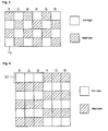
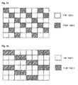
- the switching frequency f of the data driver IC is highest when the data pattern has alternating High and Low logic levels in adjacent discharge cells in both the column and row direction, as illustrated in FIG. 3.
- the data pattern illustrated in FIG. 3 requires the data driver IC to repeatedly turn on and off a switching element with ever horizontal signal.
- the switching frequency f of the data driver IC is also high when the data pattern has alternating High and Low logic levels in adjacent pixel cells in both the column and row direction, as illustrated in FIG. 4, where a pixel cell 20 includes for example, a red sub-pixel R, a green sub-pixel G, and a blue sub-pixel.
- a pixel cell 20 includes for example, a red sub-pixel R, a green sub-pixel G, and a blue sub-pixel.
- the data pattern illustrated in FIG. 3 requires the data driver IC to repeatedly turn on and off a switching element which every horizontal signal.
- the present invention is directed to a data control unit for a plasma display panel and method of using same that substantially obviates one or more of the problems due to limitations and disadvantages of the related art.
- a plasma display apparatus including scan electrodes and data electrodes intersecting the scan electrodes, the apparatus comprises a scan driving unit that scans the scan electrodes according to a scan sequence; a data driving unit that supplies a data signal corresponding to the scan sequence to the data electrodes; and a control unit that controls the scan driver and the data driver; the control unit controlling the scan driver in order to perform a first scan for sequentially scanning odd numbered scan electrodes, and a second scan for sequentially scanning even numbered scan electrodes, when input data includes a data pattern which repeats a logical inversion for cells in a column direction.
- FIG. 5 illustrates a data control unit for a plasma display panel according to an embodiment of the present invention.
- the data control unit includes a first reverse gamma controller (41A), a data aligner (46), and a gain controller (42), an error diffuser (43), a subfield mapping unit (44), and a data pattern detector (45) connected between the first reverse gamma controller (41A) and the data aligner (46).
- the data control unit includes a second reverse gamma controller (41 B), a waveform generator (48), and an APL calculator (47) connected between the second reverse gamma controller (41 B) and the waveform generator (48).
- the first and second reverse gamma controllers (41A and 41 B) reverse gamma correct digital video data R,G,B received from input line (40) to linearly convert brightness for the gray level value of a video signal.
- the gain controller (42) compensates for color variation due to temperature by controlling the effective gain of red, green and blue data.
- the error diffuser (43) minutely controls brightness by diffusing the quantum error of the digital video data RGB received from the gain controller (42).
- the subfield mapping unit (44) maps the data received from the error diffuser (43) to pre-stored subfield bit patterns, and supplies the mapped data to the data pattern detector (45).
- the dat pattern detector (45) detects predefined data patterns based on the bits mapped to each subfield and supplies a control signal corresponding to the detected data pattern to the waveform generator (48) and the data aligner (46).
- the waveform generator (48) controls the scan sequence so as to correspond to the control signal supplied from the data pattern detector (45). Accordingly, the scan sequence may be different for each sub-field.
- the data aligner (46) supplies the digital video data inputted from the subfield mapping unit (44) to a data driver (50) of the panel (49).
- the data aligner (46) controls the supply sequence of the data such that it corresponds to the control signal supplied from the data pattern detector (45).
- the APL calculator (47) calculates an average brightness on a screen basis for the digital video data RGB inputted from the second reverse correction part (41 B), i.e., an average picture level (APL), and outputs the information regarding the number of sustain pulses corresponding to the calculated APL.
- APL average picture level
- the waveform generator (48) responds to the sustain pulse information from the APL calclulator (47) to generate a timing control signal, and supplies the generated timing control signal to the panel (49).
- the panel (49) displays a picture corresponding to the data supplied from the data aligner (46). For this, a data driver (50) and a scan driver (52), illustrated in FIG. 6, are connected to the panel (49).
- the data driver (50) converts the data supplied from the data aligner (46) into a data signal, and supplies the converted data signal to the data electrodes (X1 to Xn).
- the scan driver (52) responds to the control signal supplied from the waveform generator 48 to supply a scan pulse to the scan electrodes (Y1 to Ym).
- the scan pulses may be applied to each scan electrode sequentially, or the scan electrodes (Y1 to Ym) may be divided into two or more blocks in response to the control signal and the scan pulses may be applied to each block sequentially.
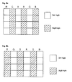
- the data pattern detector (45) determines if the detected data pattern comprises a repeating pattern of high and low logic between each discharge cell (10) or each pixel cell (20) in both the column and row direction as illustrated in FIGs. 3 and 4. It should be noted that although the present invention is described with regard to only the data patterns illustrated in FIGs. 3 and 4, other repeating data patterns may exsist and be detected.
- the data pattern detector (45) supplies a general pattern control signal to the waveform generator (48) and the data aligner (46).
- the waveform generator (48) receiving the general pattern control signal controls the scan driver (52) such that a scan pulse is sequentially supplied to the first scan electrode (Y1) to the m th scan electrode (Ym).
- the data aligner (46) receiving the general pattern control signal aligns the data and supplies the aligned data to the data driver (50) such that the data signal is sequentially supplied to the discharge cells connected to the first scan electrode (Y1) to the discharge cells connected to the m th scan electrode (Ym).
- the data pattern detector (45) supplies a repeat pattern control signal to the waveform generator (48) and the data aligner (46).
- the waveform generator (48) When the waveform generator (48) receives a repeat pattern control signal it controls the scan driver (52) so that scan pulses are supplied to scan electrodes (Y1 to Ym) in a predefined scan sequence associated with the repeating pattern. For example, if either of the patterns illustrated in FIGS. 3 and 4 are detected, the scan electrodes are divided into two blocks, and the scan pulses are supplied to each scan eletrode within a block sequentially. More specifically, the scan driver (52) divides the scan electrodes into odd numbered scan electrodes (Y1, Y3, Y5,...) and even numbered scan electrodes (Y2, Y4, Y6,...) by the control of the waveform generator (48).
- a scan pulse is squentially to each of the odd numbered scan electrodes, then a scan pulse is sequentially supplied to the even numbered scan electroes, or vice versa. It does not make a difference which block of scan electrodes comes first between the step of scanning the odd numbered scan electrodes and the step of scanning the even numbered scan electrodes.
- the data aligner (46) receiving the repeat pattern control signal alignes the data to correspond to the scan sequence and supplies the aligned data to the data driver (50).
- the data aligner (46) supplies the data corresponding to the odd numbered scan electrodes (Y1, Y3, Y5,....), and then supplies the data corresponding to the even numbered scan electrodes (Y2, Y4, Y6,).
- the data driver (50) converts the data supplied from the data aligner (46) into the data signal and supplies the converted data signal to the data electrodes (X1 to Xn).
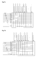
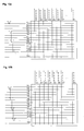
- the scan driver (52) supplies the scan pulse to the odd numbered scan electrodes (Y1, Y3, Y5,%), as illustrated in FIG. 7A, then the even numbered scan electrodes (Y2, Y4, Y6,%) as illustrated in FIGs. 7B.
- the scan pulse When the scan pulse is supplied to the odd numbered scan electrodes (Y1, Y3, Y5,...), the data signal of the same polarity is supplied to each of the data electrodes (X1 to Xn), as illustrated in FIG. 7A.
- the polarity of the data signal supplied to each of the data electrodes (X1 to Xn) does not change each horizontal signals, but rather maintains the same polaity until the scan pulse is supplied to all the odd numbered scan electrodes (Y1, Y3, Y5, ...) as illustrated in FIG. 8A.
- the scan driver (52) sequentially supplies the scan pulse to the even numbered scan electrodes (Y2, Y4, Y6, ...) as illustrated in FIG. 7B. Accordingly, the polarity of the data signal supplied to each of the data electrodes (X1 to Xn) does not change each horizontal signal, but rather maintains the same polarity until the scan pulse is supplied to all the even numbered scan electrodes (Y2, Y4, Y6, ...) as illustrated in FIG. 8B.
- the polarity of the data signal supplied to the data electrodes (X1 to Xn) is changed only when the scan pulse is supplied to the first even numbered scan electrode (Y2) after the scan pulse is supplied to the last odd numbered scan electrode (Ym-1 ), and it maintains the same polarity elsewhere.
- the switching devices of the data driver (50) maintains the same state (on or off state) during the period when the scan pulse is supplied to all the odd numbered scan electrodes (Y1, Y3, Y5,...) and during the period when the scan pulse is supplied to the all the even numbered scan electrodes (Y2, Y4, Y6,). Accordingly, power consumption is reduced and it is possible to prevent high heat from being generated in the data driver (50).
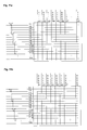
- the scan driver (52) supplies the scan pluse to the odd numbered scan electrodes (Y1, Y3, Y5, ...) and the even numbered scan electrodes (Y2, Y4, Y6,...) as illustrated in FIGs. 9A and 9B.
- the scan pulse is supplied to the odd numbered scan electrodes (Y1, Y3, Y5, ...) as in FIG. 9A
- the data signal of the same polarity (high or low) is supplied to each of the data electrodes (X1 to Xn).
- the polarity of the data signal supplied to each of the data electrodes (X1 to Xn) does not change each horizontal signal, but rather maintains the same polarity until the scan pulse is supplied to all the odd numbered scan electrodes (Y1, Y3, Y5, ...) as illustrated in FIG. 10A.
- the scan driver (52) sequentially supplies the scan pulse to the even numbered scan electrodes (Y2, Y4, Y6, ...) as illustrated in FIG. 9B.
- the data driver (50) supplies the data signal having the same polarity to each of the data electrodes (X1 to Xn). In other words, the polarity of the data signal supplied to each of the data electrodes (X1 to Xn) does not change each horizontal signal, but rather maintains the same polarity until the scan pulse is supplied to all the even numbered scan electrodes (Y2, Y4, Y6, ...) as illustrated in FIG. 10B.
- the polarity of the data signal supplied to the data electrodes (X1 to Xn) changes only when the scan pulse is supplied to the first even numbered scan electrode (Y2) after the scan pulse is supplied to the last odd numbered scan electrode (Ym-1), and it maintains the same polarity elsewhere.
- the switching devices of the data driver (50) maintains the same on or off state (high or low state) during the period when the scan pulse is supplied to all the odd numbered scan electrodes (Y1, Y3, Y5,...) and the period when the scan pulse is supplied to the all the even numbered scan electrodes (Y2, Y4, Y6,). Accordingly, power consumption is reduced and it is possible to prevent high heat from being generated in the data driver (50).
- the scan electrodes are divided into two blocks and the scan pulse is sequentially supplied to each of the blocks.
- the scan electrodes may be divided into more that two blocks.
- the scan electrodes (Y1 to Ym) may be divided into four blocks to receive the scan pulses.
- the waveform generator (48) receiving the repeat pattern control signal from the data pattern detector (45) divides the scan electrodes (Y1 to Ym) into four blocks and controls the scan driver (52) so that the scan pulse is sequentially supplied to each of the four blocks.
- the scan electrodes (Y1 to Ym) are divided into a first block (Y1, Y5, Y9, ...) including the i th (where i is 1, 5, 9, 13, ...) scan electrodes Yi, a second block (Y2, Y6, Y10, ...) including the (i+1) th scan electrodes (Yi+1), a third block (Y3, Y7, Y11, ...) including (i+2) th scan electrodes (Yi+2), and a fourth block (Y4, Y8, Y12, ...) including (i+3) th scan electrodes (Yi+3).
- the scan driver (52) sequentially supplies the scan pulse to the scan electrodes included in each of the first, second, third, and fourth blocks. That is, the scan driver (52) executes the step of continuously scanning the scan electrodes included in the first block, the step of continuously scanning the scan electrodes inlcuded in the second block, the step of continuously scanning the scan electrodes included in the third block, and the step of continuously scanning the scan electrodes inlcuded in the fourth block.
- the data aligner (46) receiving the repeat pattern control signal aligns the data to correspond to the scan sequence and supplies the aligned data to the data driver (50). In other words, the data aligner (46) supplies the data corresponding the specific scan sequence to the data driver (50).
- the scan driver (52) supplies a scan pulse to the i th scan electrode (Yi), the (i+1) th scan electrode (Yi+1), the (i+2) th scan electrode (Yi+2), and the (i+3) th scan electrode (Yi+3) as illustrated in FIGs. 11A to 11D.
- the polarity of the data signal supplied to each of the data electrodes (X1 to Xn) is changed when the scan pulse is supplied to the first (i+1) th scan electrode (Yi+1) (the first scan electrode of the second block), the first (i+2) th scan electrode (Yi+2) (the first scan electrode of the third block) and the first (i+3) th scan electrode (Yi+3) (the first scan electrode of the fourth block), but maintains the same polarity in the other cases.
- the scan driver (52) supplies the scan pulse dividedly to the i th scan electrode (Yi), (i+1) th scan electrode (Yi+1), (i+2) th scan electrode (Yi+2), (i+3) th scan electrode (Yi+3) as shown in FIGs. 12A to 12D.
- the polarity of the data signal supplied to each of the data electrodes (X1 to Xn) is changed when the scan pulse is supplied to the the first (i+1) th scan electrode (Yi+1) (the first scan electrode of the second block), the first (i+2) th scan electrode (Yi+2) (the first scan electrode of the third block) and the first (i+3) th scan electrode (Yi+3) (the first scan electrode of the fourth block), but maintains the same polarity in the other cases.
- the present invention may be applicable to other block configurations having the same repeat data pattern [(0, 1, 0, 1, 0, 1) and (1, 0, 1, 0, 1, 0)] but not having equal spacings, as well as the (Y1, Y5, Y9, ...), (Y2, Y6, Y10, %), (Y3, Y7, Y11, ...), (Y4, Y8, Y12, %) block configuration explained in FIGs. 11 to 12.
- the block composition of the odd numbered scan electrode to which the same repeat data pattern is applied might be made as in (Y3, Y7, Y9, Y11, ...), (Y5, Y13, Y17, Y19, ...) and (Y1, Y15, Y21, Y25, ). Further, the number of the scan electrode included in each block might be the same or different.
Landscapes
- Engineering & Computer Science (AREA)
- Physics & Mathematics (AREA)
- Power Engineering (AREA)
- Plasma & Fusion (AREA)
- Computer Hardware Design (AREA)
- General Physics & Mathematics (AREA)
- Theoretical Computer Science (AREA)
- Control Of Indicators Other Than Cathode Ray Tubes (AREA)
- Control Of Gas Discharge Display Tubes (AREA)
Applications Claiming Priority (1)
| Application Number | Priority Date | Filing Date | Title |
|---|---|---|---|
| KR1020040073104A KR20060024215A (ko) | 2004-09-13 | 2004-09-13 | 플라즈마 디스플레이 패널의 데이터 제어방법 및 장치 |
Publications (2)
| Publication Number | Publication Date |
|---|---|
| EP1635316A2 true EP1635316A2 (de) | 2006-03-15 |
| EP1635316A3 EP1635316A3 (de) | 2006-08-02 |
Family
ID=36158530
Family Applications (1)
| Application Number | Title | Priority Date | Filing Date |
|---|---|---|---|
| EP05253936A Ceased EP1635316A3 (de) | 2004-09-13 | 2005-06-24 | Datensteuergerät für eine Plasmaanzeigetafel und Verfahren zur Verwendung dieses Datensteuergeräts |
Country Status (6)
| Country | Link |
|---|---|
| US (1) | US20060055634A1 (de) |
| EP (1) | EP1635316A3 (de) |
| JP (1) | JP2006079063A (de) |
| KR (1) | KR20060024215A (de) |
| CN (1) | CN1750079A (de) |
| TW (1) | TW200609873A (de) |
Cited By (1)
| Publication number | Priority date | Publication date | Assignee | Title |
|---|---|---|---|---|
| EP1772842A1 (de) * | 2005-10-07 | 2007-04-11 | LG Electronics Inc. | Plasmaanzeigegerät und Steuerverfahren dafür |
Families Citing this family (8)
| Publication number | Priority date | Publication date | Assignee | Title |
|---|---|---|---|---|
| KR100737184B1 (ko) | 2005-09-23 | 2007-07-10 | 엘지전자 주식회사 | 플라즈마 디스플레이 장치 및 그의 구동 방법 |
| JP2008268794A (ja) * | 2007-04-25 | 2008-11-06 | Matsushita Electric Ind Co Ltd | プラズマディスプレイ装置の駆動方法 |
| KR100917735B1 (ko) * | 2007-11-28 | 2009-09-15 | 삼성에스디아이 주식회사 | 플라즈마 표시 장치 및 그의 구동 방법 |
| WO2009096186A1 (ja) * | 2008-01-31 | 2009-08-06 | Panasonic Corporation | プラズマディスプレイ装置 |
| JP5652002B2 (ja) * | 2009-11-13 | 2015-01-14 | セイコーエプソン株式会社 | 電気泳動表示装置、電気泳動表示装置の駆動方法、コントローラ、電子機器 |
| KR101445338B1 (ko) * | 2009-12-24 | 2014-10-01 | 주식회사 오리온 | 플라즈마 디스플레이 패널의 구동 장치 및 방법 |
| WO2012098903A1 (ja) * | 2011-01-20 | 2012-07-26 | パナソニック株式会社 | 画像表示装置および画像表示装置の駆動方法 |
| WO2012098902A1 (ja) * | 2011-01-20 | 2012-07-26 | パナソニック株式会社 | 画像表示装置および画像表示装置の駆動方法 |
Family Cites Families (6)
| Publication number | Priority date | Publication date | Assignee | Title |
|---|---|---|---|---|
| JP3403635B2 (ja) * | 1998-03-26 | 2003-05-06 | 富士通株式会社 | 表示装置および該表示装置の駆動方法 |
| EP1277194A1 (de) * | 2000-04-26 | 2003-01-22 | Ultrachip, Inc. | Leistungsarmes ansteuerschema für flüssigkristallanzeigevorrichtung |
| JP2002221935A (ja) * | 2000-11-24 | 2002-08-09 | Mitsubishi Electric Corp | 表示装置 |
| TW552576B (en) * | 2002-05-29 | 2003-09-11 | Au Optronics Corp | Flat panel display driving device and method |
| EP1414011A1 (de) * | 2002-10-22 | 2004-04-28 | STMicroelectronics S.r.l. | Verfahren zur Abtastfolgeselektion für Anzeigegeräte |
| KR100553206B1 (ko) * | 2004-02-19 | 2006-02-22 | 삼성에스디아이 주식회사 | 플라즈마 디스플레이 패널의 구동 장치 및 플라즈마디스플레이 패널의 화상 처리 방법 |
-
2004
- 2004-09-13 KR KR1020040073104A patent/KR20060024215A/ko not_active Ceased
-
2005
- 2005-06-21 TW TW094120630A patent/TW200609873A/zh unknown
- 2005-06-22 US US11/157,980 patent/US20060055634A1/en not_active Abandoned
- 2005-06-24 EP EP05253936A patent/EP1635316A3/de not_active Ceased
- 2005-06-29 JP JP2005190730A patent/JP2006079063A/ja active Pending
- 2005-06-29 CN CNA2005100823103A patent/CN1750079A/zh active Pending
Cited By (2)
| Publication number | Priority date | Publication date | Assignee | Title |
|---|---|---|---|---|
| EP1772842A1 (de) * | 2005-10-07 | 2007-04-11 | LG Electronics Inc. | Plasmaanzeigegerät und Steuerverfahren dafür |
| US8026868B2 (en) | 2005-10-07 | 2011-09-27 | Lg Electronics Inc. | Plasma display apparatus and method of driving the same |
Also Published As
| Publication number | Publication date |
|---|---|
| EP1635316A3 (de) | 2006-08-02 |
| US20060055634A1 (en) | 2006-03-16 |
| TW200609873A (en) | 2006-03-16 |
| JP2006079063A (ja) | 2006-03-23 |
| CN1750079A (zh) | 2006-03-22 |
| KR20060024215A (ko) | 2006-03-16 |
Similar Documents
| Publication | Publication Date | Title |
|---|---|---|
| US7936320B2 (en) | Driving method of plasma display panel and display device thereof | |
| US6344841B1 (en) | Method for driving a plasma display panel having multiple drivers for odd and even numbered electrode lines | |
| KR100825164B1 (ko) | 플라즈마 디스플레이 장치의 구동 방법 및 플라즈마디스플레이 장치 | |
| US6362800B1 (en) | Method and apparatus for driving plasma display panel | |
| EP1808843A1 (de) | Plasmaanzeigevorrichtung und Verfahren zu ihrer Ansteuerung | |
| US20050127846A1 (en) | Apparatus and method for driving plasma display panel | |
| CN100392706C (zh) | 驱动等离子显示板的设备和在其上显示画面的方法 | |
| US7598931B2 (en) | Scan driving control of a plasma display according to a predetermined data pattern | |
| EP1635316A2 (de) | Datensteuergerät für eine Plasmaanzeigetafel und Verfahren zur Verwendung dieses Datensteuergeräts | |
| CN100369090C (zh) | 等离子显示板的驱动装置及其灰度级表示方法 | |
| JP2006146217A (ja) | プラズマ表示装置及びその駆動方法 | |
| US20080150929A1 (en) | Plasma display device and driving method thereof | |
| KR100645791B1 (ko) | 플라즈마 디스플레이 패널의 구동방법 | |
| EP1580714A2 (de) | Gerät und Verfahren zum Steuern einer Plasmaanzeige | |
| EP1748408A2 (de) | Ansteuerverfahren für eine Plasmaanzeigevorrichtung | |
| US20050264486A1 (en) | Plasma display panel and driving method thereof | |
| KR100502898B1 (ko) | 플라즈마 표시 패널 및 그의 구동방법 | |
| JP2006071774A (ja) | 表示パネルの駆動装置 | |
| KR100826191B1 (ko) | 평판 디스플레이의 고해상도 인터레이스 스캔 방법 및 그평판 디스플레이 장치 | |
| KR20000001748A (ko) | 플라즈마 디스플레이 패널의 구동장치 및 방법 | |
| CN101364377A (zh) | 等离子体显示器及其驱动方法 | |
| KR20080013532A (ko) | 플라즈마 표시 장치 및 그 구동방법 | |
| KR20050036587A (ko) | 플라즈마 디스플레이 패널 및 그의 구동장치 및 구동 방법 | |
| KR20050039217A (ko) | 플라즈마 디스플레이 패널 및 그의 구동 방법 | |
| KR20070099844A (ko) | 플라즈마 표시 장치 및 그 구동 방법 |
Legal Events
| Date | Code | Title | Description |
|---|---|---|---|
| PUAI | Public reference made under article 153(3) epc to a published international application that has entered the european phase |
Free format text: ORIGINAL CODE: 0009012 |
|
| AK | Designated contracting states |
Kind code of ref document: A2 Designated state(s): AT BE BG CH CY CZ DE DK EE ES FI FR GB GR HU IE IS IT LI LT LU MC NL PL PT RO SE SI SK TR |
|
| AX | Request for extension of the european patent |
Extension state: AL BA HR LV MK YU |
|
| PUAL | Search report despatched |
Free format text: ORIGINAL CODE: 0009013 |
|
| AK | Designated contracting states |
Kind code of ref document: A3 Designated state(s): AT BE BG CH CY CZ DE DK EE ES FI FR GB GR HU IE IS IT LI LT LU MC NL PL PT RO SE SI SK TR |
|
| AX | Request for extension of the european patent |
Extension state: AL BA HR LV MK YU |
|
| 17P | Request for examination filed |
Effective date: 20060803 |
|
| 17Q | First examination report despatched |
Effective date: 20060911 |
|
| AKX | Designation fees paid |
Designated state(s): DE FR GB NL |
|
| STAA | Information on the status of an ep patent application or granted ep patent |
Free format text: STATUS: THE APPLICATION HAS BEEN REFUSED |
|
| 18R | Application refused |
Effective date: 20080126 |