EP1637498B1 - MOS Transistor mit verformbaren Gate - Google Patents
MOS Transistor mit verformbaren Gate Download PDFInfo
- Publication number
- EP1637498B1 EP1637498B1 EP05108509A EP05108509A EP1637498B1 EP 1637498 B1 EP1637498 B1 EP 1637498B1 EP 05108509 A EP05108509 A EP 05108509A EP 05108509 A EP05108509 A EP 05108509A EP 1637498 B1 EP1637498 B1 EP 1637498B1
- Authority
- EP
- European Patent Office
- Prior art keywords
- transistor
- gate
- channel area
- substrate
- source
- Prior art date
- Legal status (The legal status is an assumption and is not a legal conclusion. Google has not performed a legal analysis and makes no representation as to the accuracy of the status listed.)
- Expired - Lifetime
Links
Images

Classifications
-
- G—PHYSICS
- G01—MEASURING; TESTING
- G01P—MEASURING LINEAR OR ANGULAR SPEED, ACCELERATION, DECELERATION, OR SHOCK; INDICATING PRESENCE, ABSENCE, OR DIRECTION, OF MOVEMENT
- G01P15/00—Measuring acceleration; Measuring deceleration; Measuring shock, i.e. sudden change of acceleration
- G01P15/02—Measuring acceleration; Measuring deceleration; Measuring shock, i.e. sudden change of acceleration by making use of inertia forces using solid seismic masses
- G01P15/08—Measuring acceleration; Measuring deceleration; Measuring shock, i.e. sudden change of acceleration by making use of inertia forces using solid seismic masses with conversion into electric or magnetic values
- G01P15/12—Measuring acceleration; Measuring deceleration; Measuring shock, i.e. sudden change of acceleration by making use of inertia forces using solid seismic masses with conversion into electric or magnetic values by alteration of electrical resistance
- G01P15/124—Measuring acceleration; Measuring deceleration; Measuring shock, i.e. sudden change of acceleration by making use of inertia forces using solid seismic masses with conversion into electric or magnetic values by alteration of electrical resistance by semiconductor devices comprising at least one PN junction, e.g. transistors
-
- B—PERFORMING OPERATIONS; TRANSPORTING
- B81—MICROSTRUCTURAL TECHNOLOGY
- B81B—MICROSTRUCTURAL DEVICES OR SYSTEMS, e.g. MICROMECHANICAL DEVICES
- B81B3/00—Devices comprising flexible or deformable elements, e.g. comprising elastic tongues or membranes
- B81B3/0035—Constitution or structural means for controlling the movement of the flexible or deformable elements
-
- G—PHYSICS
- G01—MEASURING; TESTING
- G01L—MEASURING FORCE, STRESS, TORQUE, WORK, MECHANICAL POWER, MECHANICAL EFFICIENCY, OR FLUID PRESSURE
- G01L1/00—Measuring force or stress, in general
- G01L1/005—Measuring force or stress, in general by electrical means and not provided for in G01L1/06 - G01L1/22
-
- G—PHYSICS
- G01—MEASURING; TESTING
- G01L—MEASURING FORCE, STRESS, TORQUE, WORK, MECHANICAL POWER, MECHANICAL EFFICIENCY, OR FLUID PRESSURE
- G01L9/00—Measuring steady of quasi-steady pressure of fluid or fluent solid material by electric or magnetic pressure-sensitive elements; Transmitting or indicating the displacement of mechanical pressure-sensitive elements, used to measure the steady or quasi-steady pressure of a fluid or fluent solid material, by electric or magnetic means
- G01L9/0098—Measuring steady of quasi-steady pressure of fluid or fluent solid material by electric or magnetic pressure-sensitive elements; Transmitting or indicating the displacement of mechanical pressure-sensitive elements, used to measure the steady or quasi-steady pressure of a fluid or fluent solid material, by electric or magnetic means using semiconductor body comprising at least one PN junction as detecting element
-
- H—ELECTRICITY
- H03—ELECTRONIC CIRCUITRY
- H03B—GENERATION OF OSCILLATIONS, DIRECTLY OR BY FREQUENCY-CHANGING, BY CIRCUITS EMPLOYING ACTIVE ELEMENTS WHICH OPERATE IN A NON-SWITCHING MANNER; GENERATION OF NOISE BY SUCH CIRCUITS
- H03B5/00—Generation of oscillations using amplifier with regenerative feedback from output to input
- H03B5/08—Generation of oscillations using amplifier with regenerative feedback from output to input with frequency-determining element comprising lumped inductance and capacitance
- H03B5/12—Generation of oscillations using amplifier with regenerative feedback from output to input with frequency-determining element comprising lumped inductance and capacitance active element in amplifier being semiconductor device
-
- H—ELECTRICITY
- H03—ELECTRONIC CIRCUITRY
- H03B—GENERATION OF OSCILLATIONS, DIRECTLY OR BY FREQUENCY-CHANGING, BY CIRCUITS EMPLOYING ACTIVE ELEMENTS WHICH OPERATE IN A NON-SWITCHING MANNER; GENERATION OF NOISE BY SUCH CIRCUITS
- H03B5/00—Generation of oscillations using amplifier with regenerative feedback from output to input
- H03B5/08—Generation of oscillations using amplifier with regenerative feedback from output to input with frequency-determining element comprising lumped inductance and capacitance
- H03B5/12—Generation of oscillations using amplifier with regenerative feedback from output to input with frequency-determining element comprising lumped inductance and capacitance active element in amplifier being semiconductor device
- H03B5/1237—Generation of oscillations using amplifier with regenerative feedback from output to input with frequency-determining element comprising lumped inductance and capacitance active element in amplifier being semiconductor device comprising means for varying the frequency of the generator
-
- H—ELECTRICITY
- H03—ELECTRONIC CIRCUITRY
- H03B—GENERATION OF OSCILLATIONS, DIRECTLY OR BY FREQUENCY-CHANGING, BY CIRCUITS EMPLOYING ACTIVE ELEMENTS WHICH OPERATE IN A NON-SWITCHING MANNER; GENERATION OF NOISE BY SUCH CIRCUITS
- H03B5/00—Generation of oscillations using amplifier with regenerative feedback from output to input
- H03B5/30—Generation of oscillations using amplifier with regenerative feedback from output to input with frequency-determining element being electromechanical resonator
-
- B—PERFORMING OPERATIONS; TRANSPORTING
- B81—MICROSTRUCTURAL TECHNOLOGY
- B81B—MICROSTRUCTURAL DEVICES OR SYSTEMS, e.g. MICROMECHANICAL DEVICES
- B81B2201/00—Specific applications of microelectromechanical systems
- B81B2201/02—Sensors
- B81B2201/0228—Inertial sensors
- B81B2201/0235—Accelerometers
-
- B—PERFORMING OPERATIONS; TRANSPORTING
- B81—MICROSTRUCTURAL TECHNOLOGY
- B81B—MICROSTRUCTURAL DEVICES OR SYSTEMS, e.g. MICROMECHANICAL DEVICES
- B81B2201/00—Specific applications of microelectromechanical systems
- B81B2201/02—Sensors
- B81B2201/0264—Pressure sensors
-
- B—PERFORMING OPERATIONS; TRANSPORTING
- B81—MICROSTRUCTURAL TECHNOLOGY
- B81B—MICROSTRUCTURAL DEVICES OR SYSTEMS, e.g. MICROMECHANICAL DEVICES
- B81B2201/00—Specific applications of microelectromechanical systems
- B81B2201/02—Sensors
- B81B2201/0271—Resonators; ultrasonic resonators
-
- B—PERFORMING OPERATIONS; TRANSPORTING
- B81—MICROSTRUCTURAL TECHNOLOGY
- B81B—MICROSTRUCTURAL DEVICES OR SYSTEMS, e.g. MICROMECHANICAL DEVICES
- B81B2203/00—Basic microelectromechanical structures
- B81B2203/01—Suspended structures, i.e. structures allowing a movement
- B81B2203/0109—Bridges
Definitions
- FIG. 1 is a perspective view of a known deformable gate MOS transistor. This type of transistor is described in patent WO03 / 078299 of the Federal Polytechnic School of Lausanne entitled “PROCESS FOR MANUFACTURING MEMs", published on September 25, 2003.
- This transistor is formed in and above a semiconductor substrate 1.
- a grid beam 2 is supported at each end on pillars 3 and 4 placed on the substrate 1.
- Source / drain zones 5 and 6 formed in the substrate 1 are placed on each side of the beam 2.
- the portion of substrate located under the beam 2 comprises a channel zone 7.
- An object of the present invention is to provide a deformable gate MOS transistor which makes it possible to detect more finely the movements of its gate.
- the present invention provides a deformable gate MOS transistor formed in a semiconductor substrate, comprising source and drain regions separated by a channel zone extending in a first direction from the source to the drain and in a second direction perpendicular to the first, a grid conducting beam placed at least above of the channel zone extending in the second direction between support points placed on the substrate on each side of the channel zone, wherein the surface of the channel zone is hollow and has a shape similar to that of the grid beam when it is in maximum deflection towards the channel zone.
- the beam is a trilayer of metal, titanium and silicon nitride.
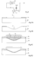
- the present invention further provides a method of manufacturing a deformable gate transistor comprising the steps of: forming by implantation in a substrate source and drain areas separated by a channel zone; deposit a protective layer on the substrate; forming an opening in the protective layer at least above the channel zone; perform a chemical-mechanical polishing of the structure previously obtained, the polishing etching process being such that it etches the substrate more than the protective layer, whereby a hollow is formed in the substrate under said opening; remove the protective layer; forming a gate oxide layer on the substrate; forming a first sacrificial portion in said recess; depositing and etching a sacrificial layer, whereby a second sacrificial portion covers the first sacrificial portion; forming a grid conducting beam passing over the second sacrificial portion and abutting the gate oxide layer on each side of the recess; eliminate the first and second sacrificial portions.
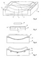
- the source / drain zones 11 and 12 have a shape identical to that of the channel zone 13. However, it will be noted that the source / drain zones 11 and 12 may have a different shape. Only the surface of the channel zone 13 must be curved in the form of a groove.
- Figure 5 is a sectional view of the transistor shown in Figure 4 in a plane perpendicular to the longitudinal axis of the gate beam 16 and substantially in the middle thereof.
- the gap between the gate beam 16 and the channel area 13 is likely to vary depending on the forces applied to the gate beam 16.
- FIGS. 6 and 7 are sectional views of the transistor shown in FIG. 4 taken along the longitudinal axis of the gate beam 16.
- the beam When no force is applied on the gate beam 16, the beam is horizontal, as this is shown in Figure 6.
- a force is applied to the beam 16, it deforms and approaches the channel zone 13.
- the deformation of the beam is important.
- the groove shape of the surface of the channel zone 13 substantially corresponds to the shape of the beam 16 when the deflection thereof is maximum. Due to this curvature of the channel area, the gap between the gate beam 16 and the channel area 13 varies little between the central portion and the side portions of the channel zone 13. Accordingly, the current is substantially identical along the entire length of the canal area. This increases the sensitivity of the transistor.
- a grid beam 38 is then formed above the sacrificial portion 37, the beam resting on the gate oxide layer 35 on each side of the sacrificial portion 37.
- This gate beam can be conventionally obtained by a deposit and etching of one or more layers of materials.
- the beam is for example made of preferably doped polycrystalline silicon or a metal / titanium / silicon nitride trilayer.
- the width of the beam is provided less than that of the hollow so that the sacrificial portion 37 is visible on each side of the gate beam 38.
- the sacrificial portions 36 and 37 are eliminated, for example by etching.
Landscapes
- Physics & Mathematics (AREA)
- General Physics & Mathematics (AREA)
- Engineering & Computer Science (AREA)
- Computer Hardware Design (AREA)
- Microelectronics & Electronic Packaging (AREA)
- Pressure Sensors (AREA)
- Insulated Gate Type Field-Effect Transistor (AREA)
Claims (7)
- In einem Halbleitersubstrat (10) ausgebildeter MOS-Transistor mit verformbarem Gate, welcher Source- und Drainzonen (11, 12) umfasst, die durch eine sich in einer ersten Richtung von der Source- zur Drainzone und in einer hierzu rechtwinkligen zweiten Richtung erstreckende Kanalzone (13) getrennt sind, sowie ein Gate (16) in Form eines leitenden Balkens, der wenigstens über der sich in der zweiten Richtung erstreckenden Kanalzone zwischen auf dem Substrat zu beiden Seiten der Kanalzone befindlichen Stütz- bzw. Auflagepunkten angeordnet ist, dadurch gekennzeichnet, dass die Oberfläche der Kanalzone eine hohle Vertiefung bzw. Mulde aufweist und eine Form ähnlicher Art wie der Gate-Leiterbalken besitzt, wenn dieser sich in maximaler Auslenkung in Richtung hin zur Kanalzone befindet.
- Transistor nach Anspruch 1, der des weiteren eine die Kanalzone (13) bedeckende Gate- Oxydschicht (14) aufweist.
- Transistor nach Anspruch 1, bei welchem der Balken (16) aus dotiertem polykristallinem Silizium besteht.
- Transistor nach Anspruch 1, bei welchem der Balken (16) ein Dreischichtgebilde aus Metall, Titan und Siliziumnitrid ist.
- Transistor nach Anspruch 1, bei welchem die Source- und die Drainzone (11, 12) eine bogenförmig gekrümmte Form gleicher Art wie die Kanalzone (13) besitzt.
- Oszillatorschaltung mit einem Transistor mit verformbarem Gate (21) nach Anspruch 1, wobei der Transistor von einem Strom durchsetzt wird, der einem Verstärker (20) zugeführt wird, dessen Ausgang dem Ausgang der Schaltung entspricht und mit dem Gate- Balken des Transistors über einen Kondensator (C) verbunden ist, wobei der Gate-Balken mit einer Vorspannungsquelle (Vpo1) verbunden ist.
- Verfahren zur Herstellung eines Transistors mit verformbarem Gate, umfassend die folgenden Schritte bzw. Stufen:in einem Substrat (30) werden mittels Implantation durch eine Kanalzone getrennte Source- und Drainbereiche ausgebildet;auf dem Substart wird eine Schutzschicht (31) abgeschieden;in der Schutzschicht wird wenigstens über der Kanalzone eine Öffnung bzw. Ausnehmung (32) gebildet;das vorstehend erhaltene Gebilde wird einem mechanisch-chemi - schen Poliervorgang unterworfen, wobei das Polier- Ätzverfahren solcher Art ist, dass es mehr das Substrat als die Schutzschicht ätzt, mit dem Ergebnis, dass in dem Substart unter der genannten Öffnung eine Vertiefung bzw. Mulde (33) gebildet wird;die Schutzschicht wird entfernt;auf dem Substrat wird eine Gate- Oxydschicht gebildet;in der genannten Vertiefung bzw. Mulde wird ein erster opferbarer Bereich (36) gebildet;Abscheiden und Ätzen einer opferbaren Schicht, mit dem Ergebnis, dass ein zweiter opferbarer Bereich den ersten opferbaren Bereich bedeckt;Bilden eines als Gate dienenden Leiterbalkens (37), der über den zweiten opferbaren Bereich führt und sich auf der Gate-Oxydschicht zu beiden Seiten der Vertiefung bzw. Mulde abstützt;der erste und der zweite Opferbereich werden entfernt
Applications Claiming Priority (1)
| Application Number | Priority Date | Filing Date | Title |
|---|---|---|---|
| FR0452070A FR2875339B1 (fr) | 2004-09-16 | 2004-09-16 | Transistor mos a grille deformable |
Publications (2)
| Publication Number | Publication Date |
|---|---|
| EP1637498A1 EP1637498A1 (de) | 2006-03-22 |
| EP1637498B1 true EP1637498B1 (de) | 2007-05-30 |
Family
ID=34948406
Family Applications (1)
| Application Number | Title | Priority Date | Filing Date |
|---|---|---|---|
| EP05108509A Expired - Lifetime EP1637498B1 (de) | 2004-09-16 | 2005-09-15 | MOS Transistor mit verformbaren Gate |
Country Status (6)
| Country | Link |
|---|---|
| US (1) | US7304358B2 (de) |
| EP (1) | EP1637498B1 (de) |
| JP (1) | JP4954518B2 (de) |
| CN (1) | CN100483740C (de) |
| DE (1) | DE602005001245T2 (de) |
| FR (1) | FR2875339B1 (de) |
Families Citing this family (12)
| Publication number | Priority date | Publication date | Assignee | Title |
|---|---|---|---|---|
| US8217381B2 (en) | 2004-06-04 | 2012-07-10 | The Board Of Trustees Of The University Of Illinois | Controlled buckling structures in semiconductor interconnects and nanomembranes for stretchable electronics |
| JP2006108378A (ja) * | 2004-10-05 | 2006-04-20 | Sony Corp | 共振トランジスタ及び通信装置 |
| KR101453419B1 (ko) * | 2006-09-06 | 2014-10-23 | 더 보오드 오브 트러스티스 오브 더 유니버시티 오브 일리노이즈 | 2차원 인장 가능하고 구부릴 수 있는 장치 |
| FR2918747A1 (fr) | 2007-07-12 | 2009-01-16 | St Microelectronics Sa | Microcapteur de pression |
| US8704314B2 (en) * | 2007-12-06 | 2014-04-22 | Massachusetts Institute Of Technology | Mechanical memory transistor |
| US8434374B2 (en) | 2008-04-11 | 2013-05-07 | Indian Institute Of Science | Sub-threshold forced plate FET sensor for sensing inertial displacements, a method and system thereof |
| JP2010123840A (ja) * | 2008-11-21 | 2010-06-03 | Fuji Electric Holdings Co Ltd | 可動ゲート型電界効果トランジスタの製造方法 |
| RU2399064C1 (ru) * | 2009-04-24 | 2010-09-10 | Общество с ограниченной ответственностью "ЭЛЕМ ИНФО" | Термочувствительный полевой прибор |
| CN102198925B (zh) * | 2010-03-25 | 2015-03-04 | 张家港丽恒光微电子科技有限公司 | Mems器件及其形成方法 |
| US9562888B2 (en) * | 2010-03-31 | 2017-02-07 | Cornell University | Stress-based sensor, method, and applications |
| US8294184B2 (en) | 2011-02-23 | 2012-10-23 | Qualcomm Mems Technologies, Inc. | EMS tunable transistor |
| RU2511203C2 (ru) * | 2012-07-31 | 2014-04-10 | Федеральное государственное автономное образовательное учреждение высшего профессионального образования "Национальный исследовательский университет "МИЭТ" (МИЭТ) | Адаптивный датчик на основе чувствительного полевого прибора |
Family Cites Families (5)
| Publication number | Priority date | Publication date | Assignee | Title |
|---|---|---|---|---|
| JPS57104269A (en) * | 1980-12-19 | 1982-06-29 | Matsushita Electric Ind Co Ltd | Load detecting element |
| US5818093A (en) * | 1996-01-25 | 1998-10-06 | Motorola, Inc. | Semiconductor device having a movable gate |
| JPH10303414A (ja) * | 1997-04-24 | 1998-11-13 | Fuji Electric Co Ltd | 絶縁ゲート型半導体装置およびそれを用いた加速度センサ |
| US6211558B1 (en) * | 1997-07-18 | 2001-04-03 | Kavlico Corporation | Surface micro-machined sensor with pedestal |
| FR2827270B1 (fr) * | 2001-07-13 | 2004-01-02 | Centre Nat Rech Scient | Procede de fabrication de pieces microscopiques |
-
2004
- 2004-09-16 FR FR0452070A patent/FR2875339B1/fr not_active Expired - Fee Related
-
2005
- 2005-09-15 DE DE602005001245T patent/DE602005001245T2/de not_active Expired - Lifetime
- 2005-09-15 US US11/227,624 patent/US7304358B2/en not_active Expired - Lifetime
- 2005-09-15 CN CNB2005101040717A patent/CN100483740C/zh not_active Expired - Fee Related
- 2005-09-15 JP JP2005268454A patent/JP4954518B2/ja not_active Expired - Lifetime
- 2005-09-15 EP EP05108509A patent/EP1637498B1/de not_active Expired - Lifetime
Non-Patent Citations (1)
| Title |
|---|
| None * |
Also Published As
| Publication number | Publication date |
|---|---|
| FR2875339A1 (fr) | 2006-03-17 |
| FR2875339B1 (fr) | 2006-12-08 |
| DE602005001245D1 (de) | 2007-07-12 |
| JP2006100819A (ja) | 2006-04-13 |
| DE602005001245T2 (de) | 2008-01-24 |
| CN100483740C (zh) | 2009-04-29 |
| US7304358B2 (en) | 2007-12-04 |
| EP1637498A1 (de) | 2006-03-22 |
| US20060054984A1 (en) | 2006-03-16 |
| CN1773725A (zh) | 2006-05-17 |
| JP4954518B2 (ja) | 2012-06-20 |
Similar Documents
| Publication | Publication Date | Title |
|---|---|---|
| EP0194953B1 (de) | Integrierter kapazitiver Sensor für mechanische Grössen und dessen Fabrikationsverfahren | |
| EP0766060B1 (de) | Herstellung eines mikromechanischen Teils mit mindestens einer Diamantspitze. | |
| EP1637498A1 (de) | MOS Transistor mit verformbaren Gate | |
| FR2778745A1 (fr) | Capteur de grandeur dynamique a semiconducteur ayant des electrodes a structure de rahmen | |
| FR2957414A1 (fr) | Capteur de force a bruit reduit | |
| EP2599745B1 (de) | Verfahren zum Herstellen eines MEMS Bauteil mit bewegliche Teile unterschiedlicher Dicke | |
| EP0983609B1 (de) | Verfahren zur herstellung eines mikrosensors mit mikrogefertigtem silizium | |
| EP2144369A1 (de) | Volumenwellenresonator | |
| EP1458095B1 (de) | Verfahren zur Herstellung eines abstimmbaren piezoelektrischen Mikroresonators | |
| FR3006113A1 (fr) | Procede de fabrication d'un capteur piezoelectrique souple | |
| EP2949621B1 (de) | Kapazitive mikro- und/ oder nanoelektronische Vorrichtung mit erhöhter Kompaktheit | |
| EP2730025B1 (de) | Volumenwellenresonator mit schwingungserregung/-erfassung | |
| FR2664979A1 (fr) | Micro-capteur de pression. | |
| EP2201681B1 (de) | Auf nanometrischem oder mikrometrischem massstab vibrierende elektromechanische komponente mit verbessertem detektionsniveau | |
| FR2883560A1 (fr) | Microsysteme electromecanique comprenant une poutre se deformant par flexion | |
| EP0392945B1 (de) | Mikromagnetometer mit kapazitiver Detektion | |
| FR3014093A1 (fr) | Systeme masse-ressort a faible debattement transverse | |
| EP1536439A1 (de) | Variablen Kondensator enthaltendes Bauteil | |
| WO2006079765A1 (fr) | Microresonateur | |
| WO2003100969A1 (fr) | Procede de realisation de structure de microsysteme a entrefers lateraux et structure de microsysteme correspondante | |
| EP4705039A1 (de) | Verfahren zur herstellung eines cmut-wandlers | |
| WO2002091556A1 (fr) | Actionneur electrostatique |
Legal Events
| Date | Code | Title | Description |
|---|---|---|---|
| PUAI | Public reference made under article 153(3) epc to a published international application that has entered the european phase |
Free format text: ORIGINAL CODE: 0009012 |
|
| AK | Designated contracting states |
Kind code of ref document: A1 Designated state(s): AT BE BG CH CY CZ DE DK EE ES FI FR GB GR HU IE IS IT LI LT LU LV MC NL PL PT RO SE SI SK TR |
|
| AX | Request for extension of the european patent |
Extension state: AL BA HR MK YU |
|
| 17P | Request for examination filed |
Effective date: 20060922 |
|
| GRAC | Information related to communication of intention to grant a patent modified |
Free format text: ORIGINAL CODE: EPIDOSCIGR1 |
|
| GRAP | Despatch of communication of intention to grant a patent |
Free format text: ORIGINAL CODE: EPIDOSNIGR1 |
|
| AKX | Designation fees paid |
Designated state(s): DE FR GB IT |
|
| GRAS | Grant fee paid |
Free format text: ORIGINAL CODE: EPIDOSNIGR3 |
|
| GRAA | (expected) grant |
Free format text: ORIGINAL CODE: 0009210 |
|
| AK | Designated contracting states |
Kind code of ref document: B1 Designated state(s): DE FR GB IT |
|
| REG | Reference to a national code |
Ref country code: GB Ref legal event code: FG4D Free format text: NOT ENGLISH |
|
| REF | Corresponds to: |
Ref document number: 602005001245 Country of ref document: DE Date of ref document: 20070712 Kind code of ref document: P |
|
| GBT | Gb: translation of ep patent filed (gb section 77(6)(a)/1977) |
Effective date: 20070705 |
|
| PLBE | No opposition filed within time limit |
Free format text: ORIGINAL CODE: 0009261 |
|
| STAA | Information on the status of an ep patent application or granted ep patent |
Free format text: STATUS: NO OPPOSITION FILED WITHIN TIME LIMIT |
|
| 26N | No opposition filed |
Effective date: 20080303 |
|
| PGFP | Annual fee paid to national office [announced via postgrant information from national office to epo] |
Ref country code: GB Payment date: 20110830 Year of fee payment: 7 Ref country code: DE Payment date: 20110902 Year of fee payment: 7 |
|
| PGFP | Annual fee paid to national office [announced via postgrant information from national office to epo] |
Ref country code: IT Payment date: 20110823 Year of fee payment: 7 |
|
| PGFP | Annual fee paid to national office [announced via postgrant information from national office to epo] |
Ref country code: FR Payment date: 20111007 Year of fee payment: 7 |
|
| GBPC | Gb: european patent ceased through non-payment of renewal fee |
Effective date: 20120915 |
|
| REG | Reference to a national code |
Ref country code: FR Ref legal event code: ST Effective date: 20130531 |
|
| PG25 | Lapsed in a contracting state [announced via postgrant information from national office to epo] |
Ref country code: DE Free format text: LAPSE BECAUSE OF NON-PAYMENT OF DUE FEES Effective date: 20130403 Ref country code: GB Free format text: LAPSE BECAUSE OF NON-PAYMENT OF DUE FEES Effective date: 20120915 |
|
| PG25 | Lapsed in a contracting state [announced via postgrant information from national office to epo] |
Ref country code: FR Free format text: LAPSE BECAUSE OF NON-PAYMENT OF DUE FEES Effective date: 20121001 Ref country code: IT Free format text: LAPSE BECAUSE OF NON-PAYMENT OF DUE FEES Effective date: 20120915 |
|
| REG | Reference to a national code |
Ref country code: DE Ref legal event code: R119 Ref document number: 602005001245 Country of ref document: DE Effective date: 20130403 |