EP1637914A1 - Lokal deformierbarer Spiegel aus elektroaktivem Material, dessen Dicke mittels elektrischen Effekten variiert werden kann - Google Patents
Lokal deformierbarer Spiegel aus elektroaktivem Material, dessen Dicke mittels elektrischen Effekten variiert werden kann Download PDFInfo
- Publication number
- EP1637914A1 EP1637914A1 EP05108640A EP05108640A EP1637914A1 EP 1637914 A1 EP1637914 A1 EP 1637914A1 EP 05108640 A EP05108640 A EP 05108640A EP 05108640 A EP05108640 A EP 05108640A EP 1637914 A1 EP1637914 A1 EP 1637914A1
- Authority
- EP
- European Patent Office
- Prior art keywords
- electrodes
- stage
- layer
- electro
- mirror according
- Prior art date
- Legal status (The legal status is an assumption and is not a legal conclusion. Google has not performed a legal analysis and makes no representation as to the accuracy of the status listed.)
- Granted
Links
Images


Classifications
-
- G—PHYSICS
- G02—OPTICS
- G02B—OPTICAL ELEMENTS, SYSTEMS OR APPARATUS
- G02B26/00—Optical devices or arrangements for the control of light using movable or deformable optical elements
- G02B26/08—Optical devices or arrangements for the control of light using movable or deformable optical elements for controlling the direction of light
-
- G—PHYSICS
- G02—OPTICS
- G02B—OPTICAL ELEMENTS, SYSTEMS OR APPARATUS
- G02B26/00—Optical devices or arrangements for the control of light using movable or deformable optical elements
- G02B26/06—Optical devices or arrangements for the control of light using movable or deformable optical elements for controlling the phase of light
-
- G—PHYSICS
- G02—OPTICS
- G02B—OPTICAL ELEMENTS, SYSTEMS OR APPARATUS
- G02B26/00—Optical devices or arrangements for the control of light using movable or deformable optical elements
- G02B26/08—Optical devices or arrangements for the control of light using movable or deformable optical elements for controlling the direction of light
- G02B26/0816—Optical devices or arrangements for the control of light using movable or deformable optical elements for controlling the direction of light by means of one or more reflecting elements
- G02B26/0825—Optical devices or arrangements for the control of light using movable or deformable optical elements for controlling the direction of light by means of one or more reflecting elements the reflecting element being a flexible sheet or membrane, e.g. for varying the focus
Definitions
- the invention relates to the field of optical instruments with high or very high resolution.
- a first disadvantage is due to the integration of the membrane on its support.
- the constraints of fixing the flexible membrane on the circular mount cause deformations that must be mechanically minimized and that can reappear under the effect of temperature variations and local temperature gradients.
- a second drawback is due to the electrostatic force applied by the actuators (or electrodes) on the membrane. Indeed, this electrostatic force being proportional to the voltage applied to the square (V2), the actuators can exert only a tensile force on the membrane which tends to bring it closer to them. It is therefore necessary to apply an offset voltage (or “offset”) to bring the plane of the membrane closer to the plane of the electrodes so as to attempt to create "bumps" on the membrane by loosening locally the force of the traction.
- This solution requires the use of part of the actuation capacity of the electrodes. Because of its strong curvature, a peripheral ring of the mirror can no longer be used for the correction of aberrations, which induces a reduction in the useful area.
- optical instruments used in the context of spatial or terrestrial observations.
- optical instruments comprise for example a telescope coupled to a deformable mirror of the type shown above.
- these optical instruments may also comprise servo-control means responsible for making measurements on the active face of their deformable mirror in order to control its shape by the voltages applied to its different electrodes.
- a deformable mirror M is intended to compensate for the geometric aberrations of an optical instrument at one of its pupils.
- the optical instrument is an observation instrument, possibly high resolution, embedded in one or more spacecraft, such as for example one or more satellites or a space shuttle, and intended to observe the earth from space.
- the luminous flux must be analyzed after crossing the instrument which introduces the geometric aberrations, but these can be corrected at any point, preferably at the exit also, for reasons of compactness.
- An image of the exit pupil of the instrument is thus made on the active face of the mirror. In this case, the bandwidth of the mirror is about a few hertz for a few tens of microns maximum deformation.
- the invention is not limited to this application. It can be used in any type of optical instrument with geometric aberrations, and in particular in the field of terrestrial astronomy (for example for the correction of the aberrations due to the atmosphere - in this case the bandwidth of the mirror is about a hundred Hertz for a few microns of deformation), or in the field of scientific instrumentation (in particular lasers, especially of power), or in the industrial field, or in the field of medical imaging (especially in ophthalmology).
- the invention can also be applied to the shape correction of a large mirror, such as a primary telescope mirror, or to each of its parts in the case of a large segmented mirror.
- the substrate S comprises a front face FAS to which the first stage E1 of plane electrodes EL is secured.
- the substrate S is preferably rigid. It is for example made of a material such as glass (for example of the ULE ® or zerodur ® type). But any other stable and electrically insulating (or insulated) material may be used, and especially carbon-carbon composite materials or sintered SiC.
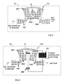
- planar electrodes EL of the first stage E1 are placed in selected places under the rear face of the first electro-active layer CP1 (opposite its front face FAE), so as to allow the deformation of selected zones of the latter, as will see it later. They are for example of hexagonal shape and arranged relative to each other so as to form a triangular tiling. But of course other forms can be envisaged for the electrodes. Similarly, any other type of electrode positioning can be envisaged, as for example that illustrated in Figure 3 which comprises forty planar and coplanar electrodes arranged within five concentric rings.
- the first stage E1 is for example a printed circuit on which are defined, in particular, the plane electrodes EL.
- the electrodes EL it is also possible to directly define the electrodes EL on the front face FAS of the substrate S, for example by vacuum deposition.
- the first electro-active layer CP1 can be produced, for example, by a spin coating technique. This technique consists of depositing a small amount of material on the surface to be covered and rotating said surface so that the material spreads homogeneously to form a layer of selected thickness.
- the electroactive layer can also be produced by liquid phase deposition. For this purpose, it is possible, for example, to apply the polymer after mixing it with a solvent, which leaves after drying a film having a good surface finish. In another variant, this film can be directly produced by spraying on the support surface.
- the number of first supply circuits C1i is preferably equal to the number of electrodes EL of the first stage E1, so as to allow the placement of each electrode under an electrical potential chosen independently of the other electrodes of the first stage E1.
- N electrodes EL can selectively deform, by controlling the N supply circuits C11 to C1 N, one to N different areas of the first electro-active layer CP1.
- At least one zone can be locally deformed by using a single EL electrode connected to a supply circuit, this is known as the "zonal" command, that is to deform all the zones by using all the N elements. electrodes respectively connected to the N supply circuits, this is called the "modal" control.
- the aberrations measured in the exit pupil, or restored from images provided by the instrument itself are first projected on the basis of n polynomials of Zernicke. (orthogonal orthogonal polynomials with two variables ⁇ and ⁇ on a disk), which offers the advantage of classifying optical instrument defects in order of decreasing influence.
- the wave area ie the aberrations
- the wave area is represented by a vector with n components which represent respectively the weights of the n polynomials in the global deformation of the wave surface (which should be to be a plan if the instrument was perfect).
- each polynomial describes a proper form that can be best achieved by sending particular voltages on N electrodes available.
- the control system therefore stores n groups of N particular voltages. By weighting each group by the n components of the vector representing the wave surface and performing the algebraic half sum for each electrode, the N deformation control voltages are obtained which best cancel the aberrations in the pupil.
- Each supply circuit C1 i is connected to the electrical ground and in contact with the front face FAC of the first electro-active layer CP1.
- This potential difference creates in the zone concerned a transverse electric field (that is to say perpendicular to the first electro-active layer CP1) which induces a local deformation by electrical effect.
- This electrical effect is more precisely an electrostriction tending to vary the thickness of the first electro-active layer.
- the reflective layer CR ensures the quality of the reflection in terms of absorbed energy, reflected energy and scattered energy, while the polish of the electro-active film (or layer) determines the optical quality of the mirror M.
- the local deformation of the first electro-active layer CP1 depends on several parameters and in particular on its thickness, on the electro-active material in which it is made and on the chosen potential difference, which also depends on its thickness. For example, for an electro-active layer CP1 fluorinated doped copolymer of 100 microns thick and a high voltage equal to about 17 kV, a deformation equal to about 7% of the thickness is obtained for an electric field of 170 MV / m, ie 7 ⁇ m of deformation.
- the voltage applied to the electrode (or electrodes) which control (s) the selected area to be deformed so as to reduce or increase the amplitude of the initial deformation is reduced or increased.
- the number of EL electrodes having a recess may vary. It can be equal to one or more within an electrode stage. In addition, it can be envisaged that the shapes of the recesses differ from one electrode to another.
- the mirror M comprises, interposed between the rear face of the first stage E1 and the front face FAS of the substrate S, a first insulating insulating layer C1, then a first intermediate conductive layer EM1 defining an electrode.
- a second electro-active layer CP2 whose rear face is secured to a second stage E2 comprising at least two planar electrodes EL, then a second insulating interlayer CI2, then a second intermediate conductive layer EM2 defining another ground electrode connected to the electrical ground, then a third electro-active layer CP3 whose rear face is secured to the front face of a third stage E3 having at least two planar electrodes EL whose rear face is secured to the front face FAS of the substrate S.
- all the ground electrodes EM1 and EM2 are electrically interconnected and all the electrodes of the same battery (ie ie belonging to different floors but placed one above the other) also.
- the plane electrodes EL of the second stage E2 may be substantially of the same shape and placed substantially in line with the electrodes of the first stage E1, just like those of the third stage E3.
- electrodes EL comprising (at least for one of those of one of the stages) one or more recesses, so as to extend the effect edge induced by the electrical effect experienced by each electro-active layer CP1, CP2, CP3.
- This third exemplary embodiment incorporates all the constituents of the first embodiment, described above with reference to FIGS. 1 to 3, and comprises, in addition, an additional AC semi-rigid and conductive (or made conductive) intermediate layer.
- This additional intermediate layer CA is interposed between the reflective layer CR, which defines a ground electrode, and the first electro-active layer CP1. It is intended to perform a spatial filtering of the deformations induced on the first electro-active layer CP1 by the first power supply circuits C1i.
- This additional intermediate layer CA is for example made of a metallic material or a semiconductor material, such as silicon.
- EL electrodes comprising, at least for one of them, one or more recesses, so as to extend the induced edge effect. by the electrical effect experienced by the first electro-active layer CP1.
- This fourth exemplary embodiment incorporates all of the constituents of the second exemplary embodiment, described above with reference to FIG. 4, and comprises in addition at least one additional intercalary CA layer that is semi-rigid and conductive (or made conductive) inserted between the reflective layer CR (defining a ground electrode) and the first electro-active layer CP1.
- This additional intermediate layer CA is identical to that described above with reference to FIG.
- the electrodes EL of the different stages can be entirely, or only partially, superimposed one above the other.
- This device Offner is intended to operate the deformable mirror M, and more specifically to make an image of the pupil of the telescope on the plane of the deformable mirror M where the wavefront correction is performed. To do this, it intercepts the entire luminous flux collected by the telescope before it reaches its focal plane.
- the device Offner DO shown comprises two deflection mirrors FM1 and FM2 and two spherical mirrors SM1 and SM2, between which is inserted the deformable mirror M according to the invention.
- observation instrument IO of FIG. 7 a local servocontrol loop intended to precisely control its different electrodes. EL.
- FIG. 8 Such an observation instrument IO is partly illustrated in FIG. 8.
- This form-correcting principle can be applied to the entire reflecting surface of a large telescope mirror coated with the electro-active material as previously indicated.
- the servo command is developed from the ideal surface (for example a parabola) that must present the reflective surface of the mirror.
- the deformations come mainly from thermal effects. On the ground, the deformations also come from the effects of gravity depending on the orientation of the telescope.
- the invention is particularly advantageous, especially for observation missions in orbit because it does not impose any moving mechanical part.
- the profile of the mirror remains unchanged (for example perfectly flat), almost without displacement of its average plane, so that the mirror does not vary the focal length of the optical instrument, which can continue to work with a small degradation of images due to the lack of compensation for its geometric aberrations.
Landscapes
- Physics & Mathematics (AREA)
- General Physics & Mathematics (AREA)
- Optics & Photonics (AREA)
- Optical Elements Other Than Lenses (AREA)
- Mechanical Light Control Or Optical Switches (AREA)
- Ultra Sonic Daignosis Equipment (AREA)
- Battery Electrode And Active Subsutance (AREA)
- Secondary Cells (AREA)
Applications Claiming Priority (1)
| Application Number | Priority Date | Filing Date | Title |
|---|---|---|---|
| FR0452092A FR2875607B1 (fr) | 2004-09-20 | 2004-09-20 | Miroir a deformation locale par variation d'epaisseur d'un materiau electro-actif controlee par effet electrique |
Publications (2)
| Publication Number | Publication Date |
|---|---|
| EP1637914A1 true EP1637914A1 (de) | 2006-03-22 |
| EP1637914B1 EP1637914B1 (de) | 2008-12-10 |
Family
ID=34948410
Family Applications (1)
| Application Number | Title | Priority Date | Filing Date |
|---|---|---|---|
| EP05108640A Expired - Lifetime EP1637914B1 (de) | 2004-09-20 | 2005-09-20 | Lokal deformierbarer Spiegel aus elektroaktivem Material, dessen Dicke mittels elektrischen Effekten variiert werden kann |
Country Status (7)
| Country | Link |
|---|---|
| US (1) | US7292385B2 (de) |
| EP (1) | EP1637914B1 (de) |
| CN (1) | CN100429555C (de) |
| AT (1) | ATE417298T1 (de) |
| DE (1) | DE602005011541D1 (de) |
| ES (1) | ES2319549T3 (de) |
| FR (1) | FR2875607B1 (de) |
Cited By (4)
| Publication number | Priority date | Publication date | Assignee | Title |
|---|---|---|---|---|
| US7292385B2 (en) * | 2004-09-20 | 2007-11-06 | Thales | Mirror with local deformation by thickness variation of an electro-active material controlled by electrical effect |
| EP1995622A1 (de) * | 2007-05-23 | 2008-11-26 | Samsung Electronics Co., Ltd | Reflektierende Einheit mit elektroaktivem Polymer und flexible Anzeige mit der reflektierenden Einheit |
| CN104613303A (zh) * | 2015-01-16 | 2015-05-13 | 西北工业大学 | 基于电活性软物质的可控面外变形单元 |
| FR3060134A1 (fr) * | 2016-12-13 | 2018-06-15 | Thales | Telescope compact presentant une pluralite de focales compense par un miroir deformable |
Families Citing this family (13)
| Publication number | Priority date | Publication date | Assignee | Title |
|---|---|---|---|---|
| US8659835B2 (en) * | 2009-03-13 | 2014-02-25 | Optotune Ag | Lens systems and method |
| US8699141B2 (en) | 2009-03-13 | 2014-04-15 | Knowles Electronics, Llc | Lens assembly apparatus and method |
| CN103119741B (zh) * | 2010-09-09 | 2015-05-20 | 皇家飞利浦电子股份有限公司 | 电活性聚合物致动器 |
| CN103513489B (zh) * | 2012-06-28 | 2016-12-21 | 中国科学院理化技术研究所 | 一种激光承载及光束变换器件 |
| CN103293662B (zh) * | 2013-06-07 | 2017-04-05 | 清华大学 | 反射式镜面面型控制装置 |
| CN103576282B (zh) * | 2013-11-13 | 2016-01-20 | 苏州大学 | 一种静电拉伸薄膜反射镜的制备方法 |
| US20160266376A1 (en) * | 2015-03-10 | 2016-09-15 | Electronics And Telecommunications Research Instit Ute | Active reflective lens and apparatus using the same |
| GB201600645D0 (en) * | 2016-01-13 | 2016-02-24 | Rolls Royce Plc | Improvements in additive layer manufacturing methods |
| JP7022127B2 (ja) * | 2016-11-21 | 2022-02-17 | コーニンクレッカ フィリップス エヌ ヴェ | 光ビーム処理デバイス |
| FR3060135A1 (fr) * | 2016-12-13 | 2018-06-15 | Thales Sa | Telescope compact presentant une pluralite de focales compense par des composants optiques aspheriques |
| CN108445601B (zh) * | 2018-02-09 | 2019-12-13 | 中国科学院长春光学精密机械与物理研究所 | 一种被动式大口径主镜支撑效果提高方法和装置 |
| US20210278740A1 (en) * | 2019-05-17 | 2021-09-09 | Koninklijke Philips N.V. | Optical beam processing device |
| CN110703428A (zh) * | 2019-10-28 | 2020-01-17 | 京东方科技集团股份有限公司 | 调光镜及其制造方法、调光装置 |
Citations (3)
| Publication number | Priority date | Publication date | Assignee | Title |
|---|---|---|---|---|
| EP0793120A1 (de) * | 1996-03-19 | 1997-09-03 | Yalestown Corporation N.V. | Bimorpher, adaptiver mosaikspiegel |
| US6464363B1 (en) * | 1999-03-17 | 2002-10-15 | Olympus Optical Co., Ltd. | Variable mirror, optical apparatus and decentered optical system which include variable mirror, variable-optical characteristic optical element or combination thereof |
| US20030166773A1 (en) * | 2002-03-01 | 2003-09-04 | Industrial Technology Research Institute | Fluoropolymer composite with high ionic conductivity |
Family Cites Families (12)
| Publication number | Priority date | Publication date | Assignee | Title |
|---|---|---|---|---|
| FR2274992A1 (fr) * | 1974-06-14 | 1976-01-09 | Thomson Csf | Convertisseur electro-optique et systeme optique d'enregistrement comportant un tel convertisseur |
| FR2453423A1 (fr) * | 1979-04-04 | 1980-10-31 | Quantel Sa | Element optique epais a courbure variable |
| US5319491A (en) * | 1990-08-10 | 1994-06-07 | Continental Typographics, Inc. | Optical display |
| US5521747A (en) * | 1993-02-22 | 1996-05-28 | Engle; Craig D. | Electronically addressed deformable media light modulator |
| US5526172A (en) * | 1993-07-27 | 1996-06-11 | Texas Instruments Incorporated | Microminiature, monolithic, variable electrical signal processor and apparatus including same |
| CN1258854A (zh) * | 1998-12-30 | 2000-07-05 | 中国科学院光电技术研究所 | 集成式多元压电变形反射镜 |
| TW442783B (en) * | 1999-07-09 | 2001-06-23 | Ind Tech Res Inst | Folding mirror |
| EP1212800B1 (de) * | 1999-07-20 | 2007-12-12 | Sri International | Elektroaktive Polymergeneratoren |
| CN1139831C (zh) * | 2001-06-05 | 2004-02-25 | 中国科学院国家天文台南京天文光学技术研究所 | 大型天文望远镜镜面位移控制系统 |
| US6749556B2 (en) * | 2002-05-10 | 2004-06-15 | Scimed Life Systems, Inc. | Electroactive polymer based artificial sphincters and artificial muscle patches |
| FR2875607B1 (fr) * | 2004-09-20 | 2006-11-24 | Cit Alcatel | Miroir a deformation locale par variation d'epaisseur d'un materiau electro-actif controlee par effet electrique |
| US7054054B1 (en) * | 2004-12-20 | 2006-05-30 | Palo Alto Research Center Incorporated | Optical modulator with a traveling surface relief pattern |
-
2004
- 2004-09-20 FR FR0452092A patent/FR2875607B1/fr not_active Expired - Fee Related
-
2005
- 2005-09-19 US US11/228,335 patent/US7292385B2/en not_active Expired - Fee Related
- 2005-09-20 EP EP05108640A patent/EP1637914B1/de not_active Expired - Lifetime
- 2005-09-20 ES ES05108640T patent/ES2319549T3/es not_active Expired - Lifetime
- 2005-09-20 DE DE602005011541T patent/DE602005011541D1/de not_active Expired - Lifetime
- 2005-09-20 CN CNB200510103379XA patent/CN100429555C/zh not_active Expired - Fee Related
- 2005-09-20 AT AT05108640T patent/ATE417298T1/de active
Patent Citations (3)
| Publication number | Priority date | Publication date | Assignee | Title |
|---|---|---|---|---|
| EP0793120A1 (de) * | 1996-03-19 | 1997-09-03 | Yalestown Corporation N.V. | Bimorpher, adaptiver mosaikspiegel |
| US6464363B1 (en) * | 1999-03-17 | 2002-10-15 | Olympus Optical Co., Ltd. | Variable mirror, optical apparatus and decentered optical system which include variable mirror, variable-optical characteristic optical element or combination thereof |
| US20030166773A1 (en) * | 2002-03-01 | 2003-09-04 | Industrial Technology Research Institute | Fluoropolymer composite with high ionic conductivity |
Non-Patent Citations (2)
| Title |
|---|
| CLAIRE DIVOUX: "A Micromachined Micromachined Deformable Deformable Mirror for Adaptive Optics", 2003, XP002323249, Retrieved from the Internet <URL:http://www-leti.cea.fr/commun/AR-2003/T3-Microsystems/17-divoux.pdf> [retrieved on 20050405] * |
| WEYRAUCH T ET AL: "Performance evaluation of micromachined mirror arrays for adaptive optics", PROCEEDINGS OF THE SPIE - THE INTERNATIONAL SOCIETY FOR OPTICAL ENGINEERING SPIE-INT. SOC. OPT. ENG USA, vol. 4124, 2000, pages 32 - 41, XP002323250, ISSN: 0277-786X * |
Cited By (7)
| Publication number | Priority date | Publication date | Assignee | Title |
|---|---|---|---|---|
| US7292385B2 (en) * | 2004-09-20 | 2007-11-06 | Thales | Mirror with local deformation by thickness variation of an electro-active material controlled by electrical effect |
| EP1995622A1 (de) * | 2007-05-23 | 2008-11-26 | Samsung Electronics Co., Ltd | Reflektierende Einheit mit elektroaktivem Polymer und flexible Anzeige mit der reflektierenden Einheit |
| CN104613303A (zh) * | 2015-01-16 | 2015-05-13 | 西北工业大学 | 基于电活性软物质的可控面外变形单元 |
| CN104613303B (zh) * | 2015-01-16 | 2017-03-22 | 西北工业大学 | 基于电活性软物质的可控面外变形单元 |
| FR3060134A1 (fr) * | 2016-12-13 | 2018-06-15 | Thales | Telescope compact presentant une pluralite de focales compense par un miroir deformable |
| EP3336595A1 (de) * | 2016-12-13 | 2018-06-20 | Thales | Kompaktes teleskop, das eine vielzahl von brennweiten aufweist, die durch einen deformierbaren spiegel kompensiert wird |
| US10976537B2 (en) | 2016-12-13 | 2021-04-13 | Thales | Compact telescope having a plurality of focal lengths compensated for by a deformable mirror |
Also Published As
| Publication number | Publication date |
|---|---|
| DE602005011541D1 (de) | 2009-01-22 |
| EP1637914B1 (de) | 2008-12-10 |
| US20070223118A1 (en) | 2007-09-27 |
| CN100429555C (zh) | 2008-10-29 |
| ES2319549T3 (es) | 2009-05-08 |
| CN1752794A (zh) | 2006-03-29 |
| FR2875607B1 (fr) | 2006-11-24 |
| ATE417298T1 (de) | 2008-12-15 |
| US7292385B2 (en) | 2007-11-06 |
| FR2875607A1 (fr) | 2006-03-24 |
Similar Documents
| Publication | Publication Date | Title |
|---|---|---|
| EP1637914B1 (de) | Lokal deformierbarer Spiegel aus elektroaktivem Material, dessen Dicke mittels elektrischen Effekten variiert werden kann | |
| EP3239671B1 (de) | Vorrichtung zur erfassung von elektromagnetischer strahlung mit einer einkapselungsstruktur, die mindestens einen interferenzfilter umfasst | |
| EP2171503B1 (de) | Optische vorrichtung mit mittel zur betätigung einer kompakten verformbaren membran | |
| EP2144105B1 (de) | Vorrichtung zum Korrigieren der optischen Fehler eines Teleskopspiegels | |
| EP2335037B1 (de) | Detektor für elektromagnetische strahlung mit mikroeinkapselung und einrichtung zum detektieren von elektromagnetischer strahlung unter verwendung solcher detektoren | |
| CA3051047A1 (fr) | Element en couches transparent a reflexion diffuse directionnelle | |
| FR2664712A1 (fr) | Dispositif de modulation optique a cellules deformables. | |
| EP2269109A1 (de) | Verbesserte membran, speziell für eine optische vorrichtung mit einer verformbaren membran | |
| CA2853751A1 (fr) | Detecteur infrarouge a base de micro-planches bolometriques suspendues | |
| EP1637854B1 (de) | Bolometrische Detektorvorrichtung für infrarote Strahlung | |
| EP3123212B1 (de) | Optische vorrichtung mit einer deformierbaren membran | |
| WO2001095614A1 (fr) | Dispositif de prise de vue embarque sur un engin spatial, engin spatial et procede de prise de vue le comprenant | |
| WO2021176181A1 (fr) | Procédé d'acquisition d'images d'une zone terrestre par un engin spatial | |
| EP3514614B1 (de) | Optische vorrichtung | |
| EP4183066B1 (de) | Verfahren zur datenübertragung durch ein raumfahrzeug mit einem laser-sendemodul | |
| WO2005026814A1 (fr) | Micro-miroir ou micro-lentille actionnable electriquement en rotation | |
| EP3764148A1 (de) | Scanner mit optischer netzeinheit mit mobiler phasensteuerung | |
| EP0861496A1 (de) | Elektrische schalvorrichtung und anzeigevorrichtung der diese schalvorrichtung verwendet | |
| EP2113756A1 (de) | Hochisolierter Wärmedetektor | |
| WO2005110848A1 (fr) | Satellite, procede et flotte de satellites d'observation d'un corps celeste | |
| EP2473824B1 (de) | Feldkompensiertes interferometer | |
| FR2615002A1 (fr) | Systeme optique de correction par reseau actif pour telescope | |
| DeNatale et al. | MEMS tunable filters for LWIR spectral imaging | |
| WO2025099071A1 (fr) | Dispositif réflecteur comprenant un détecteur, et procédé associé | |
| FR3140841A1 (fr) | module de protection et ensemble de détection pour véhicule automobile |
Legal Events
| Date | Code | Title | Description |
|---|---|---|---|
| PUAI | Public reference made under article 153(3) epc to a published international application that has entered the european phase |
Free format text: ORIGINAL CODE: 0009012 |
|
| AK | Designated contracting states |
Kind code of ref document: A1 Designated state(s): AT BE BG CH CY CZ DE DK EE ES FI FR GB GR HU IE IS IT LI LT LU LV MC NL PL PT RO SE SI SK TR |
|
| AX | Request for extension of the european patent |
Extension state: AL BA HR MK YU |
|
| 17P | Request for examination filed |
Effective date: 20060922 |
|
| 17Q | First examination report despatched |
Effective date: 20061018 |
|
| AKX | Designation fees paid |
Designated state(s): AT BE BG CH CY CZ DE DK EE ES FI FR GB GR HU IE IS IT LI LT LU LV MC NL PL PT RO SE SI SK TR |
|
| RAP1 | Party data changed (applicant data changed or rights of an application transferred) |
Owner name: ALCATEL LUCENT |
|
| 17Q | First examination report despatched |
Effective date: 20061018 |
|
| GRAP | Despatch of communication of intention to grant a patent |
Free format text: ORIGINAL CODE: EPIDOSNIGR1 |
|
| GRAS | Grant fee paid |
Free format text: ORIGINAL CODE: EPIDOSNIGR3 |
|
| GRAA | (expected) grant |
Free format text: ORIGINAL CODE: 0009210 |
|
| AK | Designated contracting states |
Kind code of ref document: B1 Designated state(s): AT BE BG CH CY CZ DE DK EE ES FI FR GB GR HU IE IS IT LI LT LU LV MC NL PL PT RO SE SI SK TR |
|
| REG | Reference to a national code |
Ref country code: GB Ref legal event code: FG4D Free format text: NOT ENGLISH |
|
| REG | Reference to a national code |
Ref country code: CH Ref legal event code: EP |
|
| REG | Reference to a national code |
Ref country code: IE Ref legal event code: FG4D Free format text: LANGUAGE OF EP DOCUMENT: FRENCH |
|
| REF | Corresponds to: |
Ref document number: 602005011541 Country of ref document: DE Date of ref document: 20090122 Kind code of ref document: P |
|
| REG | Reference to a national code |
Ref country code: SE Ref legal event code: TRGR |
|
| PG25 | Lapsed in a contracting state [announced via postgrant information from national office to epo] |
Ref country code: LT Free format text: LAPSE BECAUSE OF FAILURE TO SUBMIT A TRANSLATION OF THE DESCRIPTION OR TO PAY THE FEE WITHIN THE PRESCRIBED TIME-LIMIT Effective date: 20081210 |
|
| REG | Reference to a national code |
Ref country code: ES Ref legal event code: FG2A Ref document number: 2319549 Country of ref document: ES Kind code of ref document: T3 |
|
| PG25 | Lapsed in a contracting state [announced via postgrant information from national office to epo] |
Ref country code: PL Free format text: LAPSE BECAUSE OF FAILURE TO SUBMIT A TRANSLATION OF THE DESCRIPTION OR TO PAY THE FEE WITHIN THE PRESCRIBED TIME-LIMIT Effective date: 20081210 Ref country code: LV Free format text: LAPSE BECAUSE OF FAILURE TO SUBMIT A TRANSLATION OF THE DESCRIPTION OR TO PAY THE FEE WITHIN THE PRESCRIBED TIME-LIMIT Effective date: 20081210 Ref country code: SI Free format text: LAPSE BECAUSE OF FAILURE TO SUBMIT A TRANSLATION OF THE DESCRIPTION OR TO PAY THE FEE WITHIN THE PRESCRIBED TIME-LIMIT Effective date: 20081210 |
|
| REG | Reference to a national code |
Ref country code: IE Ref legal event code: FD4D |
|
| PG25 | Lapsed in a contracting state [announced via postgrant information from national office to epo] |
Ref country code: IE Free format text: LAPSE BECAUSE OF FAILURE TO SUBMIT A TRANSLATION OF THE DESCRIPTION OR TO PAY THE FEE WITHIN THE PRESCRIBED TIME-LIMIT Effective date: 20081210 Ref country code: EE Free format text: LAPSE BECAUSE OF FAILURE TO SUBMIT A TRANSLATION OF THE DESCRIPTION OR TO PAY THE FEE WITHIN THE PRESCRIBED TIME-LIMIT Effective date: 20081210 Ref country code: RO Free format text: LAPSE BECAUSE OF FAILURE TO SUBMIT A TRANSLATION OF THE DESCRIPTION OR TO PAY THE FEE WITHIN THE PRESCRIBED TIME-LIMIT Effective date: 20081210 Ref country code: BG Free format text: LAPSE BECAUSE OF FAILURE TO SUBMIT A TRANSLATION OF THE DESCRIPTION OR TO PAY THE FEE WITHIN THE PRESCRIBED TIME-LIMIT Effective date: 20090310 |
|
| PG25 | Lapsed in a contracting state [announced via postgrant information from national office to epo] |
Ref country code: IS Free format text: LAPSE BECAUSE OF FAILURE TO SUBMIT A TRANSLATION OF THE DESCRIPTION OR TO PAY THE FEE WITHIN THE PRESCRIBED TIME-LIMIT Effective date: 20090410 Ref country code: PT Free format text: LAPSE BECAUSE OF FAILURE TO SUBMIT A TRANSLATION OF THE DESCRIPTION OR TO PAY THE FEE WITHIN THE PRESCRIBED TIME-LIMIT Effective date: 20090511 Ref country code: CZ Free format text: LAPSE BECAUSE OF FAILURE TO SUBMIT A TRANSLATION OF THE DESCRIPTION OR TO PAY THE FEE WITHIN THE PRESCRIBED TIME-LIMIT Effective date: 20081210 |
|
| PG25 | Lapsed in a contracting state [announced via postgrant information from national office to epo] |
Ref country code: SK Free format text: LAPSE BECAUSE OF FAILURE TO SUBMIT A TRANSLATION OF THE DESCRIPTION OR TO PAY THE FEE WITHIN THE PRESCRIBED TIME-LIMIT Effective date: 20081210 |
|
| PLBE | No opposition filed within time limit |
Free format text: ORIGINAL CODE: 0009261 |
|
| STAA | Information on the status of an ep patent application or granted ep patent |
Free format text: STATUS: NO OPPOSITION FILED WITHIN TIME LIMIT |
|
| PG25 | Lapsed in a contracting state [announced via postgrant information from national office to epo] |
Ref country code: DK Free format text: LAPSE BECAUSE OF FAILURE TO SUBMIT A TRANSLATION OF THE DESCRIPTION OR TO PAY THE FEE WITHIN THE PRESCRIBED TIME-LIMIT Effective date: 20081210 |
|
| 26N | No opposition filed |
Effective date: 20090911 |
|
| PG25 | Lapsed in a contracting state [announced via postgrant information from national office to epo] |
Ref country code: MC Free format text: LAPSE BECAUSE OF NON-PAYMENT OF DUE FEES Effective date: 20090930 |
|
| PG25 | Lapsed in a contracting state [announced via postgrant information from national office to epo] |
Ref country code: GR Free format text: LAPSE BECAUSE OF FAILURE TO SUBMIT A TRANSLATION OF THE DESCRIPTION OR TO PAY THE FEE WITHIN THE PRESCRIBED TIME-LIMIT Effective date: 20090311 |
|
| PG25 | Lapsed in a contracting state [announced via postgrant information from national office to epo] |
Ref country code: LU Free format text: LAPSE BECAUSE OF NON-PAYMENT OF DUE FEES Effective date: 20090920 |
|
| PG25 | Lapsed in a contracting state [announced via postgrant information from national office to epo] |
Ref country code: HU Free format text: LAPSE BECAUSE OF FAILURE TO SUBMIT A TRANSLATION OF THE DESCRIPTION OR TO PAY THE FEE WITHIN THE PRESCRIBED TIME-LIMIT Effective date: 20090611 |
|
| PG25 | Lapsed in a contracting state [announced via postgrant information from national office to epo] |
Ref country code: CY Free format text: LAPSE BECAUSE OF FAILURE TO SUBMIT A TRANSLATION OF THE DESCRIPTION OR TO PAY THE FEE WITHIN THE PRESCRIBED TIME-LIMIT Effective date: 20081210 |
|
| REG | Reference to a national code |
Ref country code: CH Ref legal event code: PCOW Free format text: ALCATEL LUCENT;3, AVENUE OCTAVE GREARD;75007 PARIS (FR) |
|
| REG | Reference to a national code |
Ref country code: CH Ref legal event code: PCOW Free format text: NEW ADDRESS: 148/152 ROUTE DE LA REINE, 92100 BOULOGNE-BILLANCOURT (FR) |
|
| REG | Reference to a national code |
Ref country code: FR Ref legal event code: CA Effective date: 20150521 |
|
| REG | Reference to a national code |
Ref country code: FR Ref legal event code: CA Effective date: 20150521 |
|
| REG | Reference to a national code |
Ref country code: FR Ref legal event code: PLFP Year of fee payment: 11 |
|
| REG | Reference to a national code |
Ref country code: FR Ref legal event code: PLFP Year of fee payment: 12 |
|
| REG | Reference to a national code |
Ref country code: FR Ref legal event code: PLFP Year of fee payment: 13 |
|
| REG | Reference to a national code |
Ref country code: CH Ref legal event code: PCOW Free format text: NEW ADDRESS: SITE NOKIA PARIS SACLAY ROUTE DE VILLEJUST, 91620 NOZAY (FR) |
|
| REG | Reference to a national code |
Ref country code: FR Ref legal event code: PLFP Year of fee payment: 14 |
|
| PGFP | Annual fee paid to national office [announced via postgrant information from national office to epo] |
Ref country code: NL Payment date: 20180920 Year of fee payment: 14 Ref country code: TR Payment date: 20180907 Year of fee payment: 14 Ref country code: AT Payment date: 20180828 Year of fee payment: 14 Ref country code: FI Payment date: 20180910 Year of fee payment: 14 Ref country code: NL Payment date: 20180912 Year of fee payment: 14 |
|
| REG | Reference to a national code |
Ref country code: FI Ref legal event code: MAE |
|
| PG25 | Lapsed in a contracting state [announced via postgrant information from national office to epo] |
Ref country code: FI Free format text: LAPSE BECAUSE OF NON-PAYMENT OF DUE FEES Effective date: 20190920 Ref country code: SE Free format text: LAPSE BECAUSE OF NON-PAYMENT OF DUE FEES Effective date: 20190921 |
|
| REG | Reference to a national code |
Ref country code: SE Ref legal event code: EUG |
|
| REG | Reference to a national code |
Ref country code: NL Ref legal event code: MM Effective date: 20191001 |
|
| PG25 | Lapsed in a contracting state [announced via postgrant information from national office to epo] |
Ref country code: NL Free format text: LAPSE BECAUSE OF NON-PAYMENT OF DUE FEES Effective date: 20191001 |
|
| REG | Reference to a national code |
Ref country code: BE Ref legal event code: MM Effective date: 20190930 |
|
| REG | Reference to a national code |
Ref country code: AT Ref legal event code: MM01 Ref document number: 417298 Country of ref document: AT Kind code of ref document: T Effective date: 20190920 |
|
| PG25 | Lapsed in a contracting state [announced via postgrant information from national office to epo] |
Ref country code: BE Free format text: LAPSE BECAUSE OF NON-PAYMENT OF DUE FEES Effective date: 20190930 |
|
| PG25 | Lapsed in a contracting state [announced via postgrant information from national office to epo] |
Ref country code: AT Free format text: LAPSE BECAUSE OF NON-PAYMENT OF DUE FEES Effective date: 20190920 |
|
| PG25 | Lapsed in a contracting state [announced via postgrant information from national office to epo] |
Ref country code: TR Free format text: LAPSE BECAUSE OF NON-PAYMENT OF DUE FEES Effective date: 20190920 |
|
| PGFP | Annual fee paid to national office [announced via postgrant information from national office to epo] |
Ref country code: DE Payment date: 20240814 Year of fee payment: 20 |
|
| PGFP | Annual fee paid to national office [announced via postgrant information from national office to epo] |
Ref country code: GB Payment date: 20240815 Year of fee payment: 20 |
|
| PGFP | Annual fee paid to national office [announced via postgrant information from national office to epo] |
Ref country code: FR Payment date: 20240821 Year of fee payment: 20 |
|
| PGFP | Annual fee paid to national office [announced via postgrant information from national office to epo] |
Ref country code: IT Payment date: 20240830 Year of fee payment: 20 |
|
| PGFP | Annual fee paid to national office [announced via postgrant information from national office to epo] |
Ref country code: ES Payment date: 20241004 Year of fee payment: 20 |
|
| PGFP | Annual fee paid to national office [announced via postgrant information from national office to epo] |
Ref country code: CH Payment date: 20241001 Year of fee payment: 20 |
|
| REG | Reference to a national code |
Ref country code: DE Ref legal event code: R071 Ref document number: 602005011541 Country of ref document: DE |
|
| REG | Reference to a national code |
Ref country code: ES Ref legal event code: FD2A Effective date: 20250926 |
|
| REG | Reference to a national code |
Ref country code: CH Ref legal event code: PL |
|
| PG25 | Lapsed in a contracting state [announced via postgrant information from national office to epo] |
Ref country code: ES Free format text: LAPSE BECAUSE OF EXPIRATION OF PROTECTION Effective date: 20250921 |
|
| REG | Reference to a national code |
Ref country code: GB Ref legal event code: PE20 Expiry date: 20250919 |