EP1638009A2 - Modulare Elektronischekarte für ein Kommunikationsnetzwerk - Google Patents
Modulare Elektronischekarte für ein Kommunikationsnetzwerk Download PDFInfo
- Publication number
- EP1638009A2 EP1638009A2 EP05108627A EP05108627A EP1638009A2 EP 1638009 A2 EP1638009 A2 EP 1638009A2 EP 05108627 A EP05108627 A EP 05108627A EP 05108627 A EP05108627 A EP 05108627A EP 1638009 A2 EP1638009 A2 EP 1638009A2
- Authority
- EP
- European Patent Office
- Prior art keywords
- card
- electronic card
- hereinbefore
- nodes
- printed circuit
- Prior art date
- Legal status (The legal status is an assumption and is not a legal conclusion. Google has not performed a legal analysis and makes no representation as to the accuracy of the status listed.)
- Withdrawn
Links
Images

Classifications
-
- G—PHYSICS
- G06—COMPUTING OR CALCULATING; COUNTING
- G06F—ELECTRIC DIGITAL DATA PROCESSING
- G06F15/00—Digital computers in general; Data processing equipment in general
- G06F15/16—Combinations of two or more digital computers each having at least an arithmetic unit, a program unit and a register, e.g. for a simultaneous processing of several programs
- G06F15/163—Interprocessor communication
- G06F15/173—Interprocessor communication using an interconnection network, e.g. matrix, shuffle, pyramid, star, snowflake
- G06F15/17337—Direct connection machines, e.g. completely connected computers, point to point communication networks
Definitions
- the present invention concerns a modular electronic card to support and manage a plurality of calculation nodes and their interconnections, and also to manage possible connections to the outside of at least part of the calculation nodes, so as to form an expandable communication network.
- calculation node we mean a component equipped with at least a processing unit, at least a memory unit, and connection elements that allow them to be connected to the modular card and/or external components.
- HPC high performance calculation
- the network of processors is of the type with a three-dimensional (3D) topology.
- 3D applications very often the calculation node has communication channels that connect it to the six adjacent nodes; each of these interfaces in turn with its first 6 neighbours, and so on. In this way the grid with the three-dimensional topology is created, which is usually obtained physically by combining together tracks on the printed circuit, connectors and cables.
- every node must have 6 independent communication channels, 2 for each of the three fundamental directions x, y z (or x+, x-, y+, y-, z+, z-).
- the link is not of the two-directional type but there is the need to provide two different independent lines for the data that travel from one processor to the other, in one direction or the other; this means that it is necessary to manage 12 independent links for every node (2 for each of the 6 communication channels, one to manage input and one to manage output).
- the calculation nodes are arranged on a supporting structure consisting of a kind of housing with attached high-density interconnection for a certain number of calculation nodes.
- the supporting structure often consisting of an electronic card, must have characteristics of a modular nature: the final grid with three-dimensional topology of calculation nodes is thus obtained by connecting several of these supporting structure (via connector-cable-connector or connector-printed circuit-connector). Given the same dimensions of the supporting structure, the larger the number of nodes that can be housed thereon, the greater the width and speed of the links, the higher will be the density of calculation nodes of the final system and the performance obtainable in the structure itself. It must be remembered that the supporting structure in question have a certain relevance for the purposes of the functional management of the system too; since they are ordered sub-modules of the final grid, a kind of hierarchy is configured.
- housing structures cards
- applications in high performance calculations entail the presence of a high number of signals which, arranged in groups, move from one point to another, generating a sort of network of three-dimensional communication between the calculation nodes present on the supporting card; moreover, other groups of signals reach connectors, for example on board the card, which allow to couple together several supporting cards in order to obtain a grid with a 3D topology of the desired dimensions. Therefore, a high number of signals must be managed using transmission lines with controlled impedance and, if the rapid digital signals are to be managed correctly, it is necessary to have many layers available on the printed circuit, since inevitably the same will often find they have to travel in parallel mode, following the same direction.
- Purpose of the present invention is therefore to achieve a supporting and interconnecting structure (card) to manage at least 16 high performance calculation nodes arranged on a grid with a three-dimensional topology, which will allow to overcome all the disadvantages set forth above.
- the invention concerns a modular card to support and manage a plurality of calculation nodes (for example 16), interconnected with each other so as to generate a functional three-dimensional topology, which supports expansion means towards the outside for connection to one or more other analogous modular cards, or to other external systems.
- the modular card according to the invention is suitable to be part of an integrated system consisting of a very high number of calculation nodes, for example 256, 512, 1024 or more, operating in parallel in the resolution of highly complex problems, for example in the scientific field.
- the structure (card) according to the present invention is suitable to optimize the following requirements, often in conflict with each other:
- each housing for calculation node has 6x2 independent links (6 communication channels), two for each of the fundamental directions.
- Each node allows information to be transferred at an overall rate in the range of Gbyte/sec.
- the card is of the modular type: by connecting together several cards (via connector-cable-connector and connector-printed circuit-connector lines) a grid of nodes with a three-dimensional topology of the desired sizes can be obtained.
- the modular supporting card in the case of nodes characterized by 6 connection channels, each formed by 2 independent differential links with a width of 8 data bits + clock, for a total of 108 differential interconnections, the modular supporting card has a high spatial density of the calculation nodes, equal in the plane to at least 0.8 nodes per square decimeter.
- the ratio between planar surface, expressed in dm 2 , of the supporting card according to the invention (having this specification of 108 differential interconnections per node), and the number of nodes arranged thereon, is equal to 0.8. This maximization of the density of the calculation nodes allows to ensure a very high calculation capacity without at the same time increasing the bulk.
- the high density has been obtained, according to the invention, by means of a miniaturization of the calculation nodes and also of all the entities involved in the interconnection.
- the printed circuit has been designed and produced with the method of sub-groups, so as to render the management of the tracks more independent from the presence of the connection holes between the various planes of the printed circuit, in order to increase in this way the volumetric density of the interconnections.
- the production method has also provided to miniaturize the connectors used on the supporting card, for example the card-to-card connectors for housing the nodes, the card-to-cable connectors and the card-to-bottom card connectors for amplifying the network with the 3D topology to other cards.
- the connectors used on the supporting card for example the card-to-card connectors for housing the nodes, the card-to-cable connectors and the card-to-bottom card connectors for amplifying the network with the 3D topology to other cards.
- thermomechanical stability of the card in order to produce the printed circuit dielectric substrata were used, of a type easily found on the market but characterized by high temperatures of vitreous transition, in the range of 175-180°C, in order to improve the thermomechanical stability of the card as will be described in more detail hereafter.
- the modular card according to the invention was made so as to be compatible with the standard mechanics typically used in industrial and telecommunications electronics, such as sub-racks and cabinets. This has been obtained by suitably sizing the card and choosing, for the size on the surface, one of the discreet values on the scales that regulate said standards. The values chosen, with the aim of maximizing the density of the nodes, are as high as possible compatible with all the other constraints presented here.
- the modular card has bulk sizes compatible with the standard guides for cards used to accompany the insertion and withdrawal of electronic cards through the standardized guides in mechanics of industrial and telecommunications electronics (that is, racks).
- the printed circuit Since the printed circuit has to guarantee a very high number of interconnections by means of transmission lines with controlled impedance, it is necessarily of the multi-layer type and with a relatively great thickness (especially when common dielectric substrata are used); the higher the number of interconnections to be managed locally, the higher the number of layers needed and hence the greater the thickness will be.
- the relative printed circuits have been designed so as to be milled (with a control on the z axis) on the edges, with the removal of material until a thickness of 1.6 mm is reached, compatible with the guides as mentioned above.
- the printed circuit is designed so as to be thermo-mechanically balanced with respect to its median plane (symmetry of the copper distribution with respect to the plane of symmetry). This guarantees a good planarity during and after all the steps: production of the printed circuit, assembly, use.
- the planarity of the supporting card is fundamental, for example, when it has to be inserted into the rack, making the female differential connectors on board the card couple with the male ones present on the backplane printed circuit housed in the sub-rack containing the cards.
- the method has provided a non-functional distribution of the copper on the signal planes. Due to the very nature of production of the printed circuit, this makes the value of the thicknesses of the dielectric substratum stable in the various points of the card, irrespective of the density of tracks at that point. This ensures a good control of the impedance of the transmission lines, especially when they are obtained with particularly miniaturized structures and hence subject to greater criticalness.
- the card according to the invention is of the modular type and, by means of suitable differential connectors placed on board the card, the network with the 3D topology can be amplified as desired.
- a preferential solution provides that the card has an aluminum frame, designed ad hoc, including pin-type handles which, pivoting on a suitable bar present on the sub-rack, regulate the movement thereof.
- the printed circuit at the base of the card according to the invention has the following characteristics:
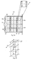
- Each calculation node 21 can be defined as an electronic card 24 on which are assembled (fig. 2) at least a processing unit 22, memory means 23 and means to assemble and connect the modular card 20.
- the modular card 20, in the preferential embodiment shown in fig. 2, functions as a support for 16 cards 24 of the type as shown in fig. 1, each one defining a calculation node 21, which form an elementary cell of the 3D topology network which can be amplified by connecting several supporting cards 20, as shown schematically in fig. 4.
- the modular card 20 has 16 housing areas 27, numbered from 0 to 15 in fig. 1, each of which is provided with connectors 26 suitable to cooperate with the connection means 25 provided on the card 24 for the assembly and electric connection of the relative calculation node 21.
- the size of the housing areas 27, like that of the reciprocal connection tracks, is optimised in order to ensure maximum possible density of the nodes, equal to at least 0.8 nodes per dm2 of planar surface of the modular card 20.
- the modular card 20 has at least two edges 28, on opposite sides, reduced in thickness by means of milling so as to reach a thickness equal to about 1.6 mm; this is to allow coupling with the standardized guides of the containing racks of the group of cards 20.
- connection means are installed in proximity with the edges, and allow the connection of the modular card 20 to the other cards which form the integrated modular system; the example shown in fig. 4 shows 16 of said cards 20, each comprising 16 calculation nodes 21, connected together in an architecture with a three-dimensional topology network, as shown in fig. 3b too.
- first connectors 30a and 30b are present for the connection to analogous modular cards 20 in a first direction, for example z-, z+, second connectors 30a and 30b for connection in a second direction, for example ⁇ -, y+, and third connectors 30c for connection in a third direction, for example x-, x+.
- a free area 31 is made, reserved for the control electronics.
- the feed modules 32 for the relative calculation nodes 21 an independent module for every node.
- the modular card 20 is made with a multi-layer obtained by means of the sub-group method and, in the case of 16 layers, is obtained by means of coupling two packets each of 8 layers.
- the modular card 20 allows to maximize the density of the calculation nodes 21, given the same bulk both in plane and also in thickness, allowing to achieve integrated systems with a very high calculation capacity.
Landscapes
- Engineering & Computer Science (AREA)
- Computer Hardware Design (AREA)
- Physics & Mathematics (AREA)
- Theoretical Computer Science (AREA)
- Mathematical Physics (AREA)
- Software Systems (AREA)
- General Engineering & Computer Science (AREA)
- General Physics & Mathematics (AREA)
- Combinations Of Printed Boards (AREA)
- Credit Cards Or The Like (AREA)
Applications Claiming Priority (1)
| Application Number | Priority Date | Filing Date | Title |
|---|---|---|---|
| IT000181A ITUD20040181A1 (it) | 2004-09-21 | 2004-09-21 | Scheda elettronica modulare per una rete di comunicazione |
Publications (2)
| Publication Number | Publication Date |
|---|---|
| EP1638009A2 true EP1638009A2 (de) | 2006-03-22 |
| EP1638009A3 EP1638009A3 (de) | 2008-07-02 |
Family
ID=34956571
Family Applications (1)
| Application Number | Title | Priority Date | Filing Date |
|---|---|---|---|
| EP05108627A Withdrawn EP1638009A3 (de) | 2004-09-21 | 2005-09-19 | Modulare Elektronischekarte für ein Kommunikationsnetzwerk |
Country Status (3)
| Country | Link |
|---|---|
| US (1) | US20060060378A1 (de) |
| EP (1) | EP1638009A3 (de) |
| IT (1) | ITUD20040181A1 (de) |
Family Cites Families (17)
| Publication number | Priority date | Publication date | Assignee | Title |
|---|---|---|---|---|
| US4000045A (en) * | 1975-01-27 | 1976-12-28 | Burroughs Corporation | Electroplating contacts of printed circuits |
| JPH0693253B2 (ja) * | 1988-06-17 | 1994-11-16 | 三菱電機株式会社 | Icメモリカード用バッテリ回路 |
| JPH04156359A (ja) * | 1990-10-19 | 1992-05-28 | Oki Electric Ind Co Ltd | 印刷装置 |
| US5734921A (en) * | 1990-11-13 | 1998-03-31 | International Business Machines Corporation | Advanced parallel array processor computer package |
| US5691885A (en) * | 1992-03-17 | 1997-11-25 | Massachusetts Institute Of Technology | Three-dimensional interconnect having modules with vertical top and bottom connectors |
| CA2211192A1 (en) * | 1995-01-25 | 1996-08-01 | Haworth, Inc. | Modular communication cabling arrangement |
| KR0174976B1 (ko) * | 1995-07-07 | 1999-04-01 | 김광호 | 확장 슬롯 전용 듀얼 버스 라이저 카드 |
| US5926378A (en) * | 1995-09-29 | 1999-07-20 | International Business Machines Corporation | Low profile riser card assembly using paired back-to-back peripheral card connectors mounted on universal footprints supporting different bus form factors |
| JP3442237B2 (ja) * | 1996-10-30 | 2003-09-02 | 株式会社日立製作所 | 間隙結合式バスシステム |
| JP3455040B2 (ja) * | 1996-12-16 | 2003-10-06 | 株式会社日立製作所 | ソースクロック同期式メモリシステムおよびメモリユニット |
| US6247078B1 (en) * | 1997-10-14 | 2001-06-12 | International Business Machines Corporation | Computer interface for integrating a first computer into a second computer |
| US5963431A (en) * | 1998-04-14 | 1999-10-05 | Compaq Computer Corporation | Desktop computer having enhanced motherboard/riser card assembly configuration |
| WO2000019292A2 (en) * | 1998-09-29 | 2000-04-06 | Evergreen Technologies, Inc. | Upgrade card for a computer system |
| US6363450B1 (en) * | 1999-03-17 | 2002-03-26 | Dell Usa, L.P. | Memory riser card for a computer system |
| US6335868B1 (en) * | 2000-02-07 | 2002-01-01 | International Business Machines Corporation | Enhanced enclosure arrangement for a computer |
| US7698723B2 (en) * | 2000-12-28 | 2010-04-13 | At&T Intellectual Property I, L.P. | System and method for multimedia on demand services |
| FR2845521B1 (fr) * | 2002-10-04 | 2005-01-07 | Wavecom | Procede et dispositif de remise en forme, notamment de remise en etat de la planeite, des elements d'interconnexion d'un module electronique, par refusion sous contrainte |
-
2004
- 2004-09-21 IT IT000181A patent/ITUD20040181A1/it unknown
-
2005
- 2005-09-19 US US11/228,330 patent/US20060060378A1/en not_active Abandoned
- 2005-09-19 EP EP05108627A patent/EP1638009A3/de not_active Withdrawn
Also Published As
| Publication number | Publication date |
|---|---|
| ITUD20040181A1 (it) | 2004-12-21 |
| US20060060378A1 (en) | 2006-03-23 |
| EP1638009A3 (de) | 2008-07-02 |
Similar Documents
| Publication | Publication Date | Title |
|---|---|---|
| EP0631678B1 (de) | Geringbenachbarte dreidimensionale verbindung. | |
| US5691885A (en) | Three-dimensional interconnect having modules with vertical top and bottom connectors | |
| US11038313B1 (en) | Orthogonal cross-connecting of printed circuit boards without a midplane board | |
| US6545895B1 (en) | High capacity SDRAM memory module with stacked printed circuit boards | |
| US5130894A (en) | Three-dimensional circuit modules | |
| US5715391A (en) | Modular and infinitely extendable three dimensional torus packaging scheme for parallel processing | |
| US9413097B2 (en) | High density cabled midplanes and backplanes | |
| US6824393B2 (en) | Fragmented backplane system for I/O applications | |
| CN107534590A (zh) | 交换机网络体系结构 | |
| US4814857A (en) | Circuit module with separate signal and power connectors | |
| CN109494218B (zh) | 双面超导量子芯片 | |
| US6800939B2 (en) | Apparatus and method for providing low-loss transmission lines in interconnected mesh plane systems | |
| US20030147376A1 (en) | Rack mounted routers | |
| CN113410053A (zh) | 一种电容器 | |
| EP1638009A2 (de) | Modulare Elektronischekarte für ein Kommunikationsnetzwerk | |
| US7800915B2 (en) | Printed board assembly | |
| US20080025007A1 (en) | Partially plated through-holes and achieving high connectivity in multilayer circuit boards using the same | |
| CN101170431B (zh) | 一种在atca系统中配置交换网络的方法及交换网络 | |
| US20020160743A1 (en) | Communication device plane having a high-speed bus | |
| US20060123021A1 (en) | Hierarchical packaging for telecommunications and computing platforms | |
| EP0276052A2 (de) | Anordnung mit Speichersystem | |
| JPH023559B2 (de) | ||
| US6965959B2 (en) | System and method for introducing proprietary signals into a standard backplane via physical separation | |
| US7525808B2 (en) | Device, system, and method of flexible hardware connectivity | |
| US12250786B2 (en) | High-speed networking device manufacturing system |
Legal Events
| Date | Code | Title | Description |
|---|---|---|---|
| PUAI | Public reference made under article 153(3) epc to a published international application that has entered the european phase |
Free format text: ORIGINAL CODE: 0009012 |
|
| AK | Designated contracting states |
Kind code of ref document: A2 Designated state(s): AT BE BG CH CY CZ DE DK EE ES FI FR GB GR HU IE IS IT LI LT LU LV MC NL PL PT RO SE SI SK TR |
|
| AX | Request for extension of the european patent |
Extension state: AL BA HR MK YU |
|
| RAP1 | Party data changed (applicant data changed or rights of an application transferred) |
Owner name: EUROTECH SPA |
|
| PUAL | Search report despatched |
Free format text: ORIGINAL CODE: 0009013 |
|
| AK | Designated contracting states |
Kind code of ref document: A3 Designated state(s): AT BE BG CH CY CZ DE DK EE ES FI FR GB GR HU IE IS IT LI LT LU LV MC NL PL PT RO SE SI SK TR |
|
| AX | Request for extension of the european patent |
Extension state: AL BA HR MK YU |
|
| AKX | Designation fees paid | ||
| REG | Reference to a national code |
Ref country code: DE Ref legal event code: 8566 |
|
| STAA | Information on the status of an ep patent application or granted ep patent |
Free format text: STATUS: THE APPLICATION IS DEEMED TO BE WITHDRAWN |
|
| 18D | Application deemed to be withdrawn |
Effective date: 20090106 |