EP1638108A1 - Mehrtor-Speicher - Google Patents
Mehrtor-Speicher Download PDFInfo
- Publication number
- EP1638108A1 EP1638108A1 EP04425692A EP04425692A EP1638108A1 EP 1638108 A1 EP1638108 A1 EP 1638108A1 EP 04425692 A EP04425692 A EP 04425692A EP 04425692 A EP04425692 A EP 04425692A EP 1638108 A1 EP1638108 A1 EP 1638108A1
- Authority
- EP
- European Patent Office
- Prior art keywords
- memory
- accordance
- core
- read
- interface device
- Prior art date
- Legal status (The legal status is an assumption and is not a legal conclusion. Google has not performed a legal analysis and makes no representation as to the accuracy of the status listed.)
- Granted
Links
- 230000015654 memory Effects 0.000 title claims abstract description 120
- 239000004065 semiconductor Substances 0.000 claims abstract description 6
- 230000003247 decreasing effect Effects 0.000 claims description 2
- 230000000875 corresponding effect Effects 0.000 claims 4
- 230000002596 correlated effect Effects 0.000 claims 2
- 238000006243 chemical reaction Methods 0.000 claims 1
- 239000000872 buffer Substances 0.000 description 7
- 230000000630 rising effect Effects 0.000 description 7
- 238000013461 design Methods 0.000 description 6
- 238000010586 diagram Methods 0.000 description 5
- 230000001360 synchronised effect Effects 0.000 description 4
- 230000002401 inhibitory effect Effects 0.000 description 3
- 230000007246 mechanism Effects 0.000 description 3
- 101150004026 SOP1 gene Proteins 0.000 description 2
- 101100366622 Saccharomyces cerevisiae (strain ATCC 204508 / S288c) SRO7 gene Proteins 0.000 description 2
- 230000004913 activation Effects 0.000 description 2
- 230000001934 delay Effects 0.000 description 2
- 230000006870 function Effects 0.000 description 2
- 238000000034 method Methods 0.000 description 2
- 238000000926 separation method Methods 0.000 description 2
- 230000005540 biological transmission Effects 0.000 description 1
- 238000004891 communication Methods 0.000 description 1
- 238000013500 data storage Methods 0.000 description 1
- 230000001419 dependent effect Effects 0.000 description 1
- 230000005764 inhibitory process Effects 0.000 description 1
- 230000003993 interaction Effects 0.000 description 1
- 230000000670 limiting effect Effects 0.000 description 1
- 238000012986 modification Methods 0.000 description 1
- 230000004048 modification Effects 0.000 description 1
- 230000008569 process Effects 0.000 description 1
- 238000012545 processing Methods 0.000 description 1
- 230000003362 replicative effect Effects 0.000 description 1
- 230000004044 response Effects 0.000 description 1
- 230000003068 static effect Effects 0.000 description 1
- 238000010200 validation analysis Methods 0.000 description 1
Images


Classifications
-
- G—PHYSICS
- G11—INFORMATION STORAGE
- G11C—STATIC STORES
- G11C7/00—Arrangements for writing information into, or reading information out from, a digital store
- G11C7/10—Input/output [I/O] data interface arrangements, e.g. I/O data control circuits, I/O data buffers
- G11C7/1075—Input/output [I/O] data interface arrangements, e.g. I/O data control circuits, I/O data buffers for multiport memories each having random access ports and serial ports, e.g. video RAM
-
- G—PHYSICS
- G11—INFORMATION STORAGE
- G11C—STATIC STORES
- G11C8/00—Arrangements for selecting an address in a digital store
- G11C8/16—Multiple access memory array, e.g. addressing one storage element via at least two independent addressing line groups
Definitions
- the present invention relates to semiconductor memories, particularly multi-port memories.
- the multi-port memories are used in a number of technological fields, mainly in the field of communication systems and multi-processor systems. Particularly, these memories are used with switching operations for telecommunications, i.e. with information transmission systems through data packs, for example in accordance with the "Ethernet" protocol.
- the multi-port memories are symmetric memories, i.e. by writing strings of N bits to memory, one can read N bits from each port.
- a four-bit data bus is the input of a dual-port memory, from these ports one can read two distinct four-bit memory locations per each clock pulse.
- the four-bit data bus also requires to be parallely written to additional memories that are similar to the previous one.
- additional memories For example, in order to have a multi-port memory with eight ports, the input data bus requires to be parallely provided to three additional dual-port memories. The contents of the start memory will be thereby replicated to these additional memories.
- multi-port memories are provided by means of elementary memory blocks each having a maximum number of ports. Consequently, one can increase the number of ports of these memories only by replicating the structures of all the above elementary multi-port memories for several times. This increases both the area occupied by the chip and the cost thereof.
- the object of the present invention is to provide an improved semiconductor memory compared to traditional multi-port memories.
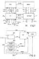
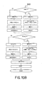
- a semiconductor memory 100 in accordance with the present invention is depicted in figure 1 by means of a block diagram.
- This memory 100 comprises a memory device CORE and an interface device IF that are capable of exchanging a plurality of data and digital information with each other.
- the memory device CORE comprises a data storage block MEM that, as is known to those skilled in the art, includes, besides a true memory array, sense amplifiers, line and column decoders, as well as input and output buffers.
- the storage block will be hereinafter called memory array MEM.
- the memory device CORE is a dual-port device (indicated with the letters A and B) comprising a memory array MEM, for example, of the SRAM type.
- this device CORE one can execute two simultaneous read operations or a write operation at each elementary operation, i.e. each access to memory array MEM.
- the present invention can also apply to the case where the memory device CORE is a one-port type or has more than two ports.
- the memory device CORE (for example, of the conventional type) comprises a first control block CM of the memory array MEM to enable write/read operations to/from the same memory array MEM.
- the interface device IF of the invention is configured such as to train the memory device CORE for several times, i.e. to access for several times the device CORE in the time domain multiplexing (TDM) to read/write from/to the memory array MEM.
- TDM time domain multiplexing
- the memory 100 of the invention is thereby faster than the clock CK and is capable of externally emulating a greater number of ports than those expected with memory device CORE.
- the interface device IF comprises input and output buffer blocks I/O BUF to receive a first QA and a second QB intermediate digital data through homonymous data buses.
- These intermediate data QA and QB are the contents of two distinct locations of array MEM that are read through both ports of the same memory array MEM at each elementary read access to the memory device CORE.
- data bus is meant a plurality of electric lines each one executing a one-bit only indicative signal.
- first SQA and second SQB validation signals being generated within the array MEM are provided to the buffer block I/O BUF via corresponding signal buses.
- the strobe signals SQA and SQB are indicative of the presence (for example, logical values 1) or absence (for example, logical values 0) of the first QA and second QB intermediate data on the ports of memory array MEM, respectively.
- the buffer block I/O BUF comprises a number NR of output buses OP 1 -OP NR to simultaneously output the intermediate data QA and QB that are read at several elementary accesses to the memory device CORE and temporarily stored in the buffer block I/O BUF.
- the output buses OP 1 -OP NR are read ports emulated by memory 100 and, advantageously, their number NR is greater than the number (equal to two, according to the example described) of buses of intermediate data QA and QB being outputted from the memory device CORE. Therefore, memory 100 allows to emulate a multi-port memory with a number NR of read output buses that is greater than the number of read data buses with which the memory array employed is provided.
- each output bus OP 1 -OP NR comprises electric lines (each one being dedicated to a bit) the number of which can be less than the number of bits (i.e. electric lines) of the bus of first QA and second QB intermediate data.
- the interface device IF comprises a second control block CI that will be hereinafter referred to as the control block CI.
- the control block CI operates by exchanging a first HSI and a second HSO handshake signals with the first control block CM of the memory device CORE. Both first HSI and second HSO handshake signals can be asserted/deasserted between two logical levels.
- the first handshake signal HSI (handshake in) is generated by the control block CI in order to be sent to the first block CM.
- This first signal HSI (for example, when it is asserted) is indicative of the beginning of an elementary access to the memory array MEM, i.e. the beginning of a read/write data operation from/to memory array MEM.
- the second handshake signal HSO (handshake out) is generated by the first control block CM in order to be sent to the control block CI.
- This second signal HSO when asserted, is indicative of the end of an elementary read/write data operation from/to the memory array MEM.
- strobe signals SQA and SQB, as well as the second handshake signal HSO are normally present in a conventional memory device CORE, but they are not made distinguishable from the outside.
- the number of assertions of the handshake signals HSI and HSO equals the number of elementary accesses to the memory device CORE that are carried out between two subsequent pulses of the digital clock signal CK.
- the handshake signals HSI and HSO allow to manage the accesses to the memory device CORE by the interface device IF in an asynchronous manner, i.e. independently from system clock signal CK.
- a new access to the device CORE will be started (with the signal HSI being asserted) only after the latter communicates (with the signal HSO asserted) that the previous access is terminated.
- the memory 100 continues to appear externally as being synchronous in accordance to the clock signal CK.
- control block CI is such to receive from the outside a plurality of NW input data buses D 1 -D NW (outlined in figure 1 with one single arrow-bus) to be written in the array MEM. These input data buses D 1 -D NW are write ports being emulated by memory 100. These input data D I -D NW are provided to the memory device CORE by means of a respective further intermediate input data bus DI.
- the intermediate input data bus DI is an input data bus for the memory device CORE.
- the total number of electric lines (each one being dedicated to one bit) of the data buses D 1 -D NW is the same as the electric lines of the intermediate input data bus DI.
- the number of electric lines of the intermediate input data bus DI is the same as the electric lines of the intermediate output data bus QA (QB). It should be observed that the total number of input/output data ports being externally emulated by memory 100 is NR + NW, where NR and NW may be different.
- control block CI is configured to receive first write enable digital signals WEN 1 -WEN NW (bit 0 or 1) and second read enable digital signals REN 1 -REN NR from the outside of memory 100.
- the number of these read/write enable signals WEN 1 -WEN NW and REN 1 -REN NR is the same as NW and NR, respectively, such as to read/write enable/disable the memory 100 as emulated.
- the control block CI provides the memory device CORE with a first MS[0] and a second MS[1] mode select binary signals, each being present on a respective electric line.
- the first mode signal MS[0] and the second mode signal MS[1] read/write enable/disable the memory device CORE according to the Table 1 below: Table 1 MS[0] MS[1] OPERATION 0 0 Read enable by means of the intermediate data buses QA and QB 0 1 Read enable by means of the intermediate data bus QB 1 0 Read enable by means of the intermediate data bus QA 1 1 Write enable by means of the bus DI
- the control block CI is such to receive first location addresses W 1 -W NW of array MEM to be written by the NW write ports and second addresses R 1 -R NR of locations to be read by the NR read ports. Particularly, these addresses are provided to the control block CI by means of NW homonymous write-dedicated address buses and NR homonymous read-dedicated address buses. For example, a bus for a plurality of respective bits is associated to the address W1 (R1) .
- the set of address buses W 1 -W NW (R 1- R NR ) is depicted in figure 1, for clarity reasons, with one arrow only.
- Each of the buses of the address bus group R 1 -R NR comprises a first group of bits (for example, the most significant ones) that are representative of the line address of the memory array MEM where there is the location to be read.
- the remainder bits of the address Rj are a second group of bits that are indicative of the particular subset of the electric lines of QA and QB which is desired to be read on the output buses OP 1 -OP NR .
- control block CI While reading, as will be better understood below, the control block CI based on said first group of bits of each address R 1 -R NR generates further address signals provided on a first line address bus RAI and a second line address bus RBI to be sent to the memory device CORE that will employ them to read corresponding locations of the memory array MEM.
- the first address bus RAI is referred to the first intermediate data bus QA and the second address bus RBI is referred to the second intermediate data bus QB.
- control block CI based on said second group of bits of each address R 1 -R NR generates first MUX_A and second MUX_B multiplexing digital signal to be sent to the buffer block I/O BUF, which will employ them to suitably send the data read on the output buses OP 1 -OP NR .
- the address signals being provided on the first line address bus RAI and second line address bus RBI are obtained from the control block CI, based on the information content of the first addresses W 1 -W NW .
- the first line addresses RAI and the second line addresses RBI are the addresses of the locations of the memory array MEM to be written.
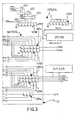
- FIG 2 A detailed structure of the interface device IF of figure 1 is illustrated in figure 2. Particularly, this figure 2 illustrates a sub-block 200, included in the interface device IF, and the memory device CORE.
- Said sub-block 200 comprises, in addition to control block CI, a digital electronic device, for example of the latch 201 type having a first input S (set input) to be activated by the clock signal CK external to memory 100, i.e. by a system clock pulse.
- One output of latch 201 is connected to the control block CI to sent to the last one an input storage signal S0P1 at a rising edge of the clock pulse CK.
- a second input R (reset) of the latch 201 can be commanded by the control block CI after the accesses to the memory array MEM are terminated.
- the sub-block 200 of the interface device IF comprises a first 202, a second 203 and a third 204 positive edge pulse generators, each of them being output connected to a first logical NAND gate 205 having three inputs.
- the clock signal CK is the input signal of the first generator 202
- the second handshake signal HSO being generated by the memory device CORE is the input signal of the second generator 203.
- the interface device IF of the invention provides a first skip signal SKIP inhibiting the execution of an elementary operation, i.e. to skip one or more accesses to the memory array MEM.
- This first signal SKIP is not explicitly shown in figure 2 and will be better detailed below.
- the interface device IF provides a second skip signal SKIPHSO to terminate an inhibition step of an elementary access.
- the third generator 204 can be controlled by the control block CI by means of said second skip signal SKIPHSO.
- the NAND gate 205 is connected to the control block CI in order to send a start signal FSMSTART to it and enable the access to the memory array MEM.
- control block CI comprises a first digital register 400a, a second digital register 400b, further first digital registers 400c, further second digital registers 400d and a third digital register 400e.
- These digital registers 400a-e are provided by logical devices of the same type and connected in cascade.
- the digital registers 400b-e can be analogous to each other and similar to register 400a that is shown in figure 4 and, therefore, only the first register 400a will be described.
- the first register 400a comprises a chain of N flip-flops 401 of type D that are cascade connected to each other.
- Each register 400a-e is a static sequential circuit in which the outputs are a function of the current inputs and also the values of the preceding inputs.
- one of the two further registers 400d can comprise a plurality of registers (each being analogous to the register from figure 4) having a respective output flip-flop connected to a corresponding electric line of the line address bus RAI and the bus relative to the first multiplexing digital signals MUX_A. Similar considerations are valid for the other register 400d being connected to the buses RBI and MUX_B.
- Each flip-flop 401 of the first register 400a from figure 4 is provided with a parallel input P i and a serial input S i (i being variable from 1 to N) that can be selected by means of the input storage signal S0P1.
- the single flip-flop 401 comprises two cascade stages: a master and a slave.
- the serial input S i is directly connected to the master stage input, whereas the parallel input P i is connected to the slave stage input.
- each flip-flop 401 (except for the last one) is output connected to the serial input of the flip-flop coming next in the chain.
- An output OUT of the last flip-flop of register 400a corresponds to a serial output of the register.
- all flip-flops 401 are controlled by the same enable signal ENABLE being provided, for example, by means of a sequence of clock pulses.
- An operation sequencer OPSEQ of the control block CI from figure 3 comprises the first 400a and second 400b registers to provide (through the respective serial outputs) a first REG_IF and a second REG_OP current status flags to a decision logic block DELOG.
- the first flag REG_IF is a bit indicating whether an elementary operation (read or write) has been carried out or not.
- the second flag REG_OP is a count bit for elementary operations, i.e. it allows to evaluate whether an elementary operation is the last operation of a cycle of accesses to the memory device CORE.
- the first register 400a is configured to store, through its parallel inputs, the first write enable digital signals WEN 1 -WEN NW and further digital signals from logic NOR gates 402 having two inputs. This NOR gates 402 are input connected to the read enable second signals REN 1 -REN NR .
- the parallel inputs of the second register 400b are connected to a power supply V DD , i.e. this register stores a logic 1 in each flip-flop in the chain.
- An address sequencer ADDSEQ of the control block CI comprises said further first registers 400c to store the write/read enable signals WEN 1 -WEN NW and REN 1 -REN NR .
- the serial outputs of the further first registers 400c are the first MS[0] and the second MS[1] selection mode signals that are indicative of the operation to be carried out by means of the ports of the memory device CORE (either read or write).
- the address sequencer ADDSEQ comprises the further second registers 400d to store the first addresses W 1 -W NW and the second addresses R 1 -R NR .
- serial outputs of the further second registers 400d are the first RAI and second RBI address buses to be sent to the memory device CORE. Furthermore, further serial outputs of registers 400d are the first MUX_A and the second MUX_B multiplexing digital signals to be sent to an output logic block OUTLOG.
- the address sequencer ADDSEQ comprises the third register 400e (for example, including several registers that are analogous to the register from figure 4) to store the input data buses D I -D NW to be provided to the device CORE by means of the intermediate input data serial bus DI.
- this decision block DELOG is a combinatory circuit and comprises first 501, second 502 and third 503 functional blocks that can be implemented by means of digital logic circuits. Furthermore, the first REG_IF and the second REG_OP status flags are the inputs of these functional blocks 501-503.
- first 501 and second 502 functional blocks can be selectively activated as a function of the logic values (0 or 1) that are taken by the flags REG_IF and REG_OP at a falling edge of the start signal FSMSTART.
- the first 501 and the second 502 functional blocks when activated, are connected to further functional blocks 504-506 (i.e. further digital circuits) to supply the first handshake signal HSI, the first SKIP and the second SKIPHSO skip signals to them.
- further functional blocks 504-506 i.e. further digital circuits
- the first skip signal SKIP contains skip information to allow shifting the addresses of the locations to be read or written in the event that one or more accesses to the memory device CORE are to be neglected.
- the third functional block 503 is activated to supply the RESET signal.
- the further first functional block 504 operates to provide a multiplexing activation signal ENMUX at a positive rising edge of the second handshake signal HSO or of the second skip signal SKIPHSO.
- the further second block 505 operates to provide an address enable signal ENADDRESS at a rising edge of the first handshake signal HSI or the first skip signal SKIP.
- This signal ENADDRESS is an enable signal of the registers 400c-e of the address sequencer ADDSEQ.
- the further third block 506 provides an operation enable signal ENOPIF at a falling edge of the first handshake signal HSI or the first skip signal SKIP.
- This signal ENOPIF is an enable signal of the registers 400a-b of the operation sequencer OPSEQ.
- the output logic block OUTLOG from figure 3 is included in the buffer block I/O BUF and can be implemented by means of a structure that is schematically illustrated in figure 6.
- the output block OUTLOG comprises first multiplexers that can be controlled through the multiplexing signals MUX_A and MUX_B to select one of the electric lines (generally indicated with QA/B 1 -QA/B mux ) of the intermediate data buses QA and QB, respectively.
- first multiplexers only one is shown that is indicated with the reference numeral 601, and to which a number of electric lines QA 1 -QA mux or a number of electric lines QB 1 -QB mux will have access.
- the output block OUTLOG comprises second multiplexers that can be controlled through the same multiplexing signals MUX_A and MUX_B to select one among the electric lines (SQA/B 1 -SQA/B mux ) of the strobe signal buses SQA and SQB, respectively.
- the output block OUTLOG comprises second multiplexers that can be controlled through the same multiplexing signals MUX_A and MUX_B to select one among the electric lines (SQA/B 1 -SQA/B mux ) of the strobe signal buses SQA and SQB, respectively.
- FIG 6 only one of said second multiplexers is shown that is designated with the reference numeral 602, and to which a number of electric lines SQA 1 -SQA mux or a number of electric lines SQB 1 -SQB mux will have access.
- sixteen multiplexers 601 are provided, each one having sixteen input electric lines.
- a first group of eight multiplexers is connected to the electric lines of the first intermediate output data bus QA and a second group of eight multiplexers is connected to the electric lines of the second intermediate output data bus QB.
- the output of each of these sixteen multiplexers is a single electric line.
- the multiplexers being associated to the electric lines of the strobe signal buses SQA and SQB.
- the electric lines of the strobe signal buses SQA and SQB are one hundred and twenty-eight (as many as the electric lines of QA and QB) and the multiplexers used are as many as those of QA and QB.
- the output block OUTLOG further comprises register means RM that are intended to store all the data being provided to the first plurality of multiplexers 601 and outputting them back on the buses OP 1 -OP NR .
- register means RM include a plurality of flip-flops (only some of which are illustrated in figure 6, with the reference numeral 604) each having an output line being an electric line of the output buses OP 1 -OP NR .
- each flip-flop 604 is connected to a respective electric line OP 11 , OP 21 , ..., OPij ,..., OP NR1 .
- NR 4 (two read elementary accesses to the memory device CORE)
- M 128 bit
- Nb 8 bit with sixteen first multiplexers 601
- thirty-two flip-flops 604 will be obtained.
- Each output bus OP 1 -OP NR provides eight flip-flops 604.
- Each first multiplexer 601 is connected to four flip-flops 604 that can be selectively enabled/disabled to store the bit being provided by the specific multiplexer 601.
- Flip-flop 604 storage enabling/disabling is carried out by means of strobe signals SQ (resulting from the selection made by the second multiplexers 602) and activation signals SA (being supplied by an output port selector OPS) that are provided to second logic NAND gates 603.
- the second multiplexer 602 is connected to second logic NAND gates 603 each having two inputs.
- the electric lines of the strobe signals SQA/SQB resulting from multiplexing are provided to one of the inputs of said NAND gates 603, whereas the other input of each gate is connected to an output port selector OPS.
- This selector OPS comprises a flip-flop shift register having the parallel inputs and the first serial input mass connected and this register being preloaded with a preset bit sequence, comprising all bits equal to a logic 1 and one single bit equal to a logic 0.
- the position of the logic 0 indicates which output flip-flop 604 is activated (through the corresponding NAND gate 603) to store the datum QA/QB from the multiplexer 601.
- the remaining output flip-flops 604 can be activated in succession as a consequence of the logic 0 shifting within said sequence in response to an enable pulse of selector OPS.
- the latch 201 deasserts the input storage signal SOP1, i.e. generates a falling edge of this signal, which is indicative that the elementary accesses have started.
- the signal S0P1 sent to the control block CI is maintained deasserted for the entire access cycle to the memory device CORE.
- All the input signals of the interface device IF i.e. the write and read enable signals WEN 1 -WEN NW and REN 1 -REN NR , the addresses W 1 -W NW and R 1 -R NR and the data D I- D NW are stored in the registers 400a-e through the respective parallel inputs. Subsequently to this storage, the registers 400a-400e are ready to provide the respective outputs in a serial manner.
- each register 400a-400e the last flip-flop in the chain causes the first parallel input to pass to the serial output without the enable signal ENABLE being applied.
- a first negative pulse of the start signal FSMSTART is generated through the first pulse generator 202 and NAND gate 205 (figure 2). Particularly, the falling edge of the start signal FSMSTART enables the decision logic DELOG.
- the first REG_IF and the second REG_OP status flags on output from the first 400a and second 400b registers, respectively, are evaluated by the decision logic DELOG. If both flags REG_IF and REG_OP take a high logic value (logic 1) the control block CI will send a first positive pulse to the memory device CORE (figure 7) of the first handshake signal HSI (handshake in), i.e. an read or write elementary operation will be started.
- This read or write elementary operation of the memory device CORE is carried out in accordance with the current values being provided on the electric lines RAI, RBI, MS [0], MS [1], DI.
- the further second functional block 505 (figure 5) generates a positive pulse of the address enable signal ENADDRESS that shifts the contents of the registers 400c-e to the serial outputs RAI, RBI, MS[0], MS[1], DI to provide the memory device CORE with the data and addresses relative to the subsequent elementary operation.
- Maximum set-up time is thereby ensured for each primary input of the memory device CORE.
- the hold time of the inputs (RAI, RBI, MS[0], MS[1], DI) of the memory device CORE requires to be near zero.
- the further third functional block 506 At the falling edge of the same pulse of the handshake signal HSI, the further third functional block 506 generates a positive pulse of the operation enable signal ENOPIF that shifts the contents of the registers 400a-b of the operation sequencer OPSEQ to provide the flags REG_IF and REG_OP relative to the subsequent operation.
- the latter Upon completion of the first elementary operation that is carried out on the memory device CORE, the latter generates a first positive pulse of the second handshake signal HSO to indicate that the read or write elementary operation is terminated (figure 7).
- This second handshake signal HSO generates, by means of the second pulse generator 203 and NAND gate 205, a second negative pulse of the start signal FSMSTART to start a second access to the device CORE through the control block CI.
- the further first functional block 501 (figure 5) generates a positive pulse of the multiplexing enable signal ENMUX (figure 9) being supplied to the registers 400d relative to the multiplexing signals MUX_A and MUX_B such as to shift the contents thereof. Therefore, the multiplexing signals for the subsequent operation are provided to the output logic block OUTLOG. The maximum set-up time is thereby ensured for all the primary inputs of the output block OUTLOG.
- the output logic block OUTLOG is enabled at the rising edge of the strobe signals SQA/B.
- the multiplexing signals MUX_A/B suitably select, by means of the first multiplexers 601 and the second multiplexers 602, particular electric lines of the intermediate data buses QA/B and the strobe signal buses SQA/B.
- the correct datum QA/B can be sampled and sent to the corresponding flip-flops 604 and then to the corresponding electric lines of the output buses OP ij . This is possible because the strobe signals SQA/B and the data QA/B are produced in a synchronous manner by the same memory device CORE.
- the maximum set-up/hold time is ensured for the output flip-flops 604. Furthermore, this maximum time is independent from the number of bits being required on the output buses OP1-OP NR , from the number of bits on the buses QA and QB of the memory device CORE and from the multiplexing factor (the number M divided by the number Nb).
- the interface device IF of the invention also provides the possibility of inhibiting the processing of one or more elementary operations on the memory device CORE by skipping to the subsequent operation/s or the end of the operation cycle.
- a positive pulse of the first skip signal SKIP (in replacement of the first handshake signal HSI) is generated.
- this skip signal SKIP is analogous to the first handshake signal HSI.
- control block CI generates a positive pulse of the second skip signal SKIPHSO (in replacement of the handshake signal HSO) to indicate that the step of inhibiting the access to the device CORE is terminated.
- this second skip signal SKIPHSO is sent to the third pulse generator 204 (figure 2) to generate a new start pulse of signal FSMSTART and to start the subsequent operation.
- control block CI At the pulse of signal FSMSTART that is generated starting from the last pulse of second handshake signal HSO, i.e. the pulse relative to the end of the last operation on the memory device CORE, the control block CI generates a reset pulse on the second input of the latch 201 that asserts the storage signal SOP1 thereby terminating the operation cycle.
- the present invention has considerable advantages over the prior art.
- the control of the elementary (read and write) operations to be carried out on the memory device is conferred only to the interface device multiplexing the external synchronization signal (clock) to obtain a further internal clock signal of the synchronous type.
- an additional circuit is used, such as for example a DLL (delay locked loop) or a PLL (phase locked loop).
- This additional circuit is sensitive to the process parameters, occupies a lot of space in the chip, emulates the maximum cycle time of the memory device without distinguishing between read and write cycles and requires an initial wait time for the phase-lock to be carried out.
- the maximum operating speed of the prior art memories is limited to the frequency field where the read/write operations on the memory device can be properly carried out, thereby avoiding undesired overrun conditions.
- the cycle time T cycle of the memory i.e. the time interval after which one can have access to the memory from the outside
- T core is a further cycle time of the memory device to which a first design margin ⁇ T is added to provide the use of a slower memory device.
- the sum T core + ⁇ T is to be multiplied by the N number of times one desires to access the memory device.
- the first margin ⁇ T is to be provided at each elementary access to the memory device.
- the accesses to the memory device CORE are also managed by the latter by means of the asynchronous handshake mechanism, i.e. with the exchange of information with the interface device IF.
- the interface device IF provides the CORE with the first handshake signal HSI and the addresses of the locations to be read/written, while it receives from the CORE the second handshake signal HSO when the read/write operations are terminated.
- This second signal HSO can be used by the interface device IF to provide the new addresses and a new first handshake signal HSI, or to skip one or more operations (through the signal SKIP), or to prepare the memory to the subsequent clock cycle if all the operations have been completed.
- the memory design is not required to provide a design margin ⁇ T per each elementary access to the device CORE.
- the additional circuits of the type DLL or PLL are not required to be introduced.
- the outputs from the memory devices are sampled by estimating an access time T aa to this device (i.e. after how much time from the access to the memory device the outputs to be sampled are made available).
- the interface device IF can quickly and properly sample the intermediate output data QA and QB by having recourse to the strobe signals SQA and SQB from the same memory device CORE, i.e. by using another handshake mechanism.
- the strobe signals SQA and SQB are locally generated to the cells of the device CORE, they are synchronous with the respective intermediate data QA and QB.
- these strobe signals SQA and SQB are additional information from the memory device CORE to indicate when these intermediate data to be sent to the output buses OP 1 -OP NR of the memory are to be sampled.
- the second margin ⁇ T' is not required to be taken into account, because the device IF operates properly regardless of the number of bits of the memory device CORE.
- the access time T aa can be minimized.
- the multi-port memory 100 of the invention is configured such as to be adaptative upon variation of the number of lines and/or columns of the memory device CORE. Therefore, a "multi-port memory family" or “memory generators” can be created (by varying words and/or bits the number of ports remaining equal) though using the same interface device IF (with the same layout) which is adaptative per se and always ensures maximum performance (by minimizing the cycle and access times) due to the handshake mechanism.
- a memory device CORE with a certain number of ports and an interface device IF like the one described above, a memory can be emulated with a greater number of ports by means of the handshake procedure without occupying a much larger chip area than that occupied by the memory device CORE.
- the multiplexing of the lines of the intermediate data buses QA and QB that is carried out within the interface device IF the number of the electric lines of the output buses OP 1 -OP NR can be considerably lower than the ones on output from the memory device CORE. Thereby, the complex signal routing required by the traditional multi-port memories, which reduces the robustness of the chip, is avoided.
- the sequential circuit blocks (registers 400a-e) and the combinatory circuit blocks (DELOG) preferably are structurally separated, i.e. they are integrating made on distinct areas being electrically connectable.
- the choice of employing a structural separation of the sequential from the combinatory blocks is advantageous compared with the choice of making the interface device IF by means of a state machine where several combinatory parts are interleaved by means of sequential parts.
- this structural separation allows a modularity of the interface device and an easier reconfigurability of the same in order to be adapted to various design requirements.
- the number of ports externally emulated by the memory 100 can be simply modified by decreasing or increasing the number of flip-flops of the sequential registers 400a-e.
Landscapes
- Engineering & Computer Science (AREA)
- Multimedia (AREA)
- Microelectronics & Electronic Packaging (AREA)
- Dram (AREA)
- Static Random-Access Memory (AREA)
Priority Applications (3)
| Application Number | Priority Date | Filing Date | Title |
|---|---|---|---|
| DE602004015288T DE602004015288D1 (de) | 2004-09-17 | 2004-09-17 | Mehrtor-Speicher |
| EP04425692A EP1638108B1 (de) | 2004-09-17 | 2004-09-17 | Mehrtor-Speicher |
| US11/228,686 US7190631B2 (en) | 2004-09-17 | 2005-09-16 | Multi-port memory |
Applications Claiming Priority (1)
| Application Number | Priority Date | Filing Date | Title |
|---|---|---|---|
| EP04425692A EP1638108B1 (de) | 2004-09-17 | 2004-09-17 | Mehrtor-Speicher |
Publications (2)
| Publication Number | Publication Date |
|---|---|
| EP1638108A1 true EP1638108A1 (de) | 2006-03-22 |
| EP1638108B1 EP1638108B1 (de) | 2008-07-23 |
Family
ID=34932767
Family Applications (1)
| Application Number | Title | Priority Date | Filing Date |
|---|---|---|---|
| EP04425692A Expired - Lifetime EP1638108B1 (de) | 2004-09-17 | 2004-09-17 | Mehrtor-Speicher |
Country Status (3)
| Country | Link |
|---|---|
| US (1) | US7190631B2 (de) |
| EP (1) | EP1638108B1 (de) |
| DE (1) | DE602004015288D1 (de) |
Families Citing this family (6)
| Publication number | Priority date | Publication date | Assignee | Title |
|---|---|---|---|---|
| KR20080008137A (ko) * | 2006-07-19 | 2008-01-23 | 삼성전자주식회사 | 영상 복원 장치 및 방법 |
| US8861304B1 (en) * | 2012-09-24 | 2014-10-14 | Altera Corporation | Circuitry for generating peak cancelling pulses |
| US9337782B1 (en) | 2014-05-21 | 2016-05-10 | Altera Corporation | Methods and apparatus for adjusting transmit signal clipping thresholds |
| KR102251809B1 (ko) * | 2014-05-28 | 2021-05-13 | 삼성전자주식회사 | 메모리 시스템, 메모리 인터페이스 장치 및 메모리 시스템에서의 인터페이싱 방법 |
| US9485129B1 (en) | 2014-07-07 | 2016-11-01 | Altera Corporation | Multi-standard peak canceling circuitry |
| US12190994B2 (en) * | 2022-12-29 | 2025-01-07 | Xilinx, Inc. | Single port memory with multiple memory operations per clock cycle |
Citations (3)
| Publication number | Priority date | Publication date | Assignee | Title |
|---|---|---|---|---|
| US5422858A (en) * | 1993-06-28 | 1995-06-06 | Hitachi, Ltd. | Semiconductor integrated circuit |
| US6317367B1 (en) * | 1997-07-16 | 2001-11-13 | Altera Corporation | FPGA with on-chip multiport memory |
| US20040107307A1 (en) * | 1998-08-10 | 2004-06-03 | Hitachi, Ltd. | Multiport memory, data processor and data processing system |
Family Cites Families (1)
| Publication number | Priority date | Publication date | Assignee | Title |
|---|---|---|---|---|
| US6629223B2 (en) * | 1998-10-06 | 2003-09-30 | Texas Instruments Incorporated | Method and apparatus for accessing a memory core multiple times in a single clock cycle |
-
2004
- 2004-09-17 DE DE602004015288T patent/DE602004015288D1/de not_active Expired - Lifetime
- 2004-09-17 EP EP04425692A patent/EP1638108B1/de not_active Expired - Lifetime
-
2005
- 2005-09-16 US US11/228,686 patent/US7190631B2/en not_active Expired - Lifetime
Patent Citations (3)
| Publication number | Priority date | Publication date | Assignee | Title |
|---|---|---|---|---|
| US5422858A (en) * | 1993-06-28 | 1995-06-06 | Hitachi, Ltd. | Semiconductor integrated circuit |
| US6317367B1 (en) * | 1997-07-16 | 2001-11-13 | Altera Corporation | FPGA with on-chip multiport memory |
| US20040107307A1 (en) * | 1998-08-10 | 2004-06-03 | Hitachi, Ltd. | Multiport memory, data processor and data processing system |
Also Published As
| Publication number | Publication date |
|---|---|
| US20060062057A1 (en) | 2006-03-23 |
| EP1638108B1 (de) | 2008-07-23 |
| US7190631B2 (en) | 2007-03-13 |
| DE602004015288D1 (de) | 2008-09-04 |
Similar Documents
| Publication | Publication Date | Title |
|---|---|---|
| CA1233259A (en) | High performance memory utilizing pipelining techniques | |
| KR100915554B1 (ko) | 반도체기억장치 | |
| US5463591A (en) | Dual port memory having a plurality of memory cell arrays for a high-speed operation | |
| JP2740063B2 (ja) | 半導体記憶装置 | |
| US6362990B1 (en) | Three port content addressable memory device and methods for implementing the same | |
| US7965568B2 (en) | Semiconductor integrated circuit device and method of testing same | |
| US20140173322A1 (en) | Packet data id generation for serially interconnected devices | |
| EP0178163B1 (de) | Digitale Speicheranordnung mit doppeltem Zugriff | |
| JP4145984B2 (ja) | 半導体記憶装置 | |
| EP0273642B1 (de) | Einrichtung zum Lesen von Daten aus einem Speicher | |
| US5787273A (en) | Multiple parallel identical finite state machines which share combinatorial logic | |
| EP1638108B1 (de) | Mehrtor-Speicher | |
| US7738496B1 (en) | Device that provides the functionality of dual-ported memory using single-ported memory for multiple clock domains | |
| US6912173B2 (en) | Method and system for fast memory access | |
| US7164607B2 (en) | Dual bus memory burst architecture | |
| JPH0730407A (ja) | プログラム可能制御、デコード及び/又はデータ操作を有するレジスタファイル | |
| US7248491B1 (en) | Circuit for and method of implementing a content addressable memory in a programmable logic device | |
| US5978295A (en) | Sequential access memories | |
| JP3746811B2 (ja) | 半導体集積回路 | |
| JP2788729B2 (ja) | 制御信号発生回路 | |
| US6442097B2 (en) | Virtual channel DRAM | |
| JP3057728B2 (ja) | 半導体記憶装置 | |
| US6222793B1 (en) | Memory devices having a restore start address counter | |
| JPH06111594A (ja) | 半導体メモリ装置 | |
| JPS6347396B2 (de) |
Legal Events
| Date | Code | Title | Description |
|---|---|---|---|
| PUAI | Public reference made under article 153(3) epc to a published international application that has entered the european phase |
Free format text: ORIGINAL CODE: 0009012 |
|
| AK | Designated contracting states |
Kind code of ref document: A1 Designated state(s): AT BE BG CH CY CZ DE DK EE ES FI FR GB GR HU IE IT LI LU MC NL PL PT RO SE SI SK TR |
|
| AX | Request for extension of the european patent |
Extension state: AL HR LT LV MK |
|
| 17P | Request for examination filed |
Effective date: 20060919 |
|
| AKX | Designation fees paid |
Designated state(s): DE FR GB IT |
|
| 17Q | First examination report despatched |
Effective date: 20061129 |
|
| GRAP | Despatch of communication of intention to grant a patent |
Free format text: ORIGINAL CODE: EPIDOSNIGR1 |
|
| GRAS | Grant fee paid |
Free format text: ORIGINAL CODE: EPIDOSNIGR3 |
|
| GRAA | (expected) grant |
Free format text: ORIGINAL CODE: 0009210 |
|
| AK | Designated contracting states |
Kind code of ref document: B1 Designated state(s): DE FR GB IT |
|
| REG | Reference to a national code |
Ref country code: GB Ref legal event code: FG4D |
|
| REF | Corresponds to: |
Ref document number: 602004015288 Country of ref document: DE Date of ref document: 20080904 Kind code of ref document: P |
|
| PLBE | No opposition filed within time limit |
Free format text: ORIGINAL CODE: 0009261 |
|
| STAA | Information on the status of an ep patent application or granted ep patent |
Free format text: STATUS: NO OPPOSITION FILED WITHIN TIME LIMIT |
|
| 26N | No opposition filed |
Effective date: 20090424 |
|
| REG | Reference to a national code |
Ref country code: FR Ref legal event code: ST Effective date: 20090529 |
|
| PG25 | Lapsed in a contracting state [announced via postgrant information from national office to epo] |
Ref country code: IT Free format text: LAPSE BECAUSE OF FAILURE TO SUBMIT A TRANSLATION OF THE DESCRIPTION OR TO PAY THE FEE WITHIN THE PRESCRIBED TIME-LIMIT Effective date: 20080723 |
|
| PG25 | Lapsed in a contracting state [announced via postgrant information from national office to epo] |
Ref country code: FR Free format text: LAPSE BECAUSE OF NON-PAYMENT OF DUE FEES Effective date: 20080930 |
|
| PGFP | Annual fee paid to national office [announced via postgrant information from national office to epo] |
Ref country code: GB Payment date: 20110830 Year of fee payment: 8 |
|
| GBPC | Gb: european patent ceased through non-payment of renewal fee |
Effective date: 20120917 |
|
| PG25 | Lapsed in a contracting state [announced via postgrant information from national office to epo] |
Ref country code: GB Free format text: LAPSE BECAUSE OF NON-PAYMENT OF DUE FEES Effective date: 20120917 |
|
| PGFP | Annual fee paid to national office [announced via postgrant information from national office to epo] |
Ref country code: DE Payment date: 20130820 Year of fee payment: 10 |
|
| REG | Reference to a national code |
Ref country code: DE Ref legal event code: R119 Ref document number: 602004015288 Country of ref document: DE |
|
| PG25 | Lapsed in a contracting state [announced via postgrant information from national office to epo] |
Ref country code: DE Free format text: LAPSE BECAUSE OF NON-PAYMENT OF DUE FEES Effective date: 20150401 |