EP1640169A2 - Dispositif pour la production d'images numériques en couleurs multiples - Google Patents
Dispositif pour la production d'images numériques en couleurs multiples Download PDFInfo
- Publication number
- EP1640169A2 EP1640169A2 EP05020623A EP05020623A EP1640169A2 EP 1640169 A2 EP1640169 A2 EP 1640169A2 EP 05020623 A EP05020623 A EP 05020623A EP 05020623 A EP05020623 A EP 05020623A EP 1640169 A2 EP1640169 A2 EP 1640169A2
- Authority
- EP
- European Patent Office
- Prior art keywords
- light
- light source
- exposure
- exposure head
- interference filter
- Prior art date
- Legal status (The legal status is an assumption and is not a legal conclusion. Google has not performed a legal analysis and makes no representation as to the accuracy of the status listed.)
- Granted
Links
- 239000000463 material Substances 0.000 claims abstract description 66
- 239000013307 optical fiber Substances 0.000 claims abstract description 55
- 238000000034 method Methods 0.000 claims abstract description 34
- 230000008878 coupling Effects 0.000 claims abstract description 14
- 238000010168 coupling process Methods 0.000 claims abstract description 14
- 238000005859 coupling reaction Methods 0.000 claims abstract description 14
- 239000003086 colorant Substances 0.000 claims abstract description 11
- 230000000295 complement effect Effects 0.000 claims abstract description 6
- 230000000694 effects Effects 0.000 claims description 18
- 230000003287 optical effect Effects 0.000 claims description 16
- 238000012937 correction Methods 0.000 claims description 14
- 239000000835 fiber Substances 0.000 claims description 14
- 230000008859 change Effects 0.000 claims description 9
- 230000008569 process Effects 0.000 claims description 8
- 238000006073 displacement reaction Methods 0.000 claims description 5
- 238000004519 manufacturing process Methods 0.000 claims description 5
- 238000003384 imaging method Methods 0.000 claims description 4
- 238000012360 testing method Methods 0.000 claims description 4
- 239000011521 glass Substances 0.000 claims description 3
- 230000009471 action Effects 0.000 claims description 2
- 239000011248 coating agent Substances 0.000 claims description 2
- 238000000576 coating method Methods 0.000 claims description 2
- 230000008901 benefit Effects 0.000 description 13
- 230000003595 spectral effect Effects 0.000 description 8
- 238000013461 design Methods 0.000 description 7
- 238000002834 transmittance Methods 0.000 description 7
- 238000011161 development Methods 0.000 description 6
- 230000018109 developmental process Effects 0.000 description 6
- 230000005540 biological transmission Effects 0.000 description 3
- 206010021703 Indifference Diseases 0.000 description 2
- 238000010586 diagram Methods 0.000 description 2
- 238000003780 insertion Methods 0.000 description 2
- 230000037431 insertion Effects 0.000 description 2
- 238000005259 measurement Methods 0.000 description 2
- 238000010521 absorption reaction Methods 0.000 description 1
- 230000003213 activating effect Effects 0.000 description 1
- 230000032683 aging Effects 0.000 description 1
- 230000015572 biosynthetic process Effects 0.000 description 1
- 238000001514 detection method Methods 0.000 description 1
Images



Classifications
-
- B—PERFORMING OPERATIONS; TRANSPORTING
- B41—PRINTING; LINING MACHINES; TYPEWRITERS; STAMPS
- B41J—TYPEWRITERS; SELECTIVE PRINTING MECHANISMS, i.e. MECHANISMS PRINTING OTHERWISE THAN FROM A FORME; CORRECTION OF TYPOGRAPHICAL ERRORS
- B41J2/00—Typewriters or selective printing mechanisms characterised by the printing or marking process for which they are designed
- B41J2/435—Typewriters or selective printing mechanisms characterised by the printing or marking process for which they are designed characterised by selective application of radiation to a printing material or impression-transfer material
- B41J2/447—Typewriters or selective printing mechanisms characterised by the printing or marking process for which they are designed characterised by selective application of radiation to a printing material or impression-transfer material using arrays of radiation sources
- B41J2/46—Typewriters or selective printing mechanisms characterised by the printing or marking process for which they are designed characterised by selective application of radiation to a printing material or impression-transfer material using arrays of radiation sources characterised by using glass fibres
Definitions
- the invention relates to an apparatus and a method for producing a multicolor image from data of a digital image on a photosensitive material, corresponding to the features in the preambles of claims 1, 24 and 33.
- the document US Pat. No. 6,452,696 B1 discloses a method and a device for controlling a plurality of light sources in a digital printer.
- Digital image data are used to expose a photosensitive material by applying light point by point to the photographic paper.
- the light pulse for exposing a pixel on the photographic paper is in each case by a light-emitting diode (LED), according to the stored digital image information, generated and passed through an optical fiber in an exposure head, through which the light pulse is finally directed to the photographic paper.
- the outlet ends of a plurality of optical fibers are in a frame of the exposure head immediately adjacent to each other, strung together.
- the arrangement of the exit ends of the optical fibers is imaged by a lens system of the exposure head on the surface of the photographic paper, so that a plurality of pixels can be exposed simultaneously.
- the exposure head is moved across the photo paper so that at the same time a plurality of parts of pixels can be created during such movement.
- the photographic paper is then advanced by a length corresponding to the number of lines first produced, whereupon a further sequence of lines of pixels, through which the exposure head moving above the paper is transferred to the photographic paper.
- correction tables can be determined by which the non-uniform exposure effect, as a function of the exposure intensity and the exposure time, can be taken into account.
- the effect is corrected which is that the exposure effect having a first exposure intensity and a first exposure time is not equal to the exposure effect achieved, for example, by half the first exposure intensity over a period of twice the first exposure time.
- This effect is also called reciprocity failure.
- other corrections are required at the edges between two strips consisting of adjacent pixel lines, which are generated by the exposure head, than is the case with pixel lines in the interior of a strip is. To avoid banding and thus impairing the image quality.
- This object of the invention is achieved by the device according to the features of claim 1.
- coupling devices are formed in the device, are connected by a respective first, a second and a third light source with a single optical fiber and thus the light of the three light sources is combined into a single optical fiber, wherein the color of the first, the second and the third light source forms a triple of complementary primary colors
- the advantage is achieved so that the exposure head only requires a third of the number of optical fibers.
- this also has the further advantage that the three colors for generating a pixel are thus applied simultaneously, and thus a higher accuracy is achieved compared to the otherwise necessary, successive exposures of the individual colors on a pixel.
- the advantage of the design of the device according to claim 2 is that due to the characteristic of the course of the spectral transmittance of the interference filter used, an optimum yield of light of the light sources used is achieved.
- the design of the device according to claim 5 has the advantage that the light sources, the interference filter and the entrance hatch of the optical fiber in the coupling unit can be arranged very compact and space-saving.
- the coupling units are arranged in a stationary light source unit, the advantage is achieved that the weight of the exposure head is thus kept as low as possible.
- the advantage is achieved that the achievable light intensities of the exposure head can be easily checked and especially when using light emitting diodes as light sources whose nonlinear relationship between Drive current and light intensity measured and in the exposure of digital images, this relationship can be considered.
- the design of the device according to claim 14 has the advantage that the outlet ends of the optical fibers do not have to be moved directly over the photosensitive material. By imaging the exit ends of the optical fibers with the proposed lens system, the inaccuracies due to the divergence of the exiting light beam from the optical fibers can be avoided.
- the mask provided according to claim 15 ensures that both the position and the shape of the pixels can be determined with high precision and mechanical inaccuracies in the assembly of the optical fibers in the exposure head are canceled out.
- the embodiment of the device according to claims 20 and 21 achieves the advantage that overlapping in the lateral direction between pixels adjacent to each other within a line is achieved in the same way as overlapping of lines or intermediate lines. The formation of vertical stripes, which could be noticeable as corresponding artifacts, are thus avoided.
- the design of the device according to claim 23 has the advantage that masks with very high precision are available with the masks formed by coated glass sheets.
- the object of the invention is solved independently by the method according to the features of claim 24.
- the advantage here is that with one third of the optical fibers, the Aus GmbH can be found and at the same time a higher accuracy of the exposure of the individual pixels of the digital image can be achieved.
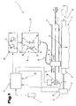
- FIG. 1 shows a device 1 for exposing a photosensitive material 2 with digital images 3 in a schematically simplified representation.
- the device 1 has for this purpose a transport device 4, with the aid of which the photosensitive material 2 can be moved in the feed direction 5.
- the photosensitive material 2 is formed by, for example, photographic paper or a film.
- a transport roller 7 operated by a motor 6 With the aid of a transport roller 7 operated by a motor 6, the material 2 is moved or positioned underneath an exposure head 8.
- the exposure head 8 can be moved back and forth along guides 9 oriented transversely or perpendicular to the feed direction 5 with the aid of an exposure head drive 10.
- the latter is alternately moved back in the direction 11 and in the direction 12, the material 2 being moved further in the feed direction 5 between the transverse movements of the exposure head 8 and being repositioned.
- There is such a line by line or pointwise exposure of the photosensitive material 2 by 8 light pulses are directed to the material 2 by the exposure head.
- the generation of the light pulses takes place in a light source unit 13 with light sources 14, 15, 16, which are preferably each formed by a light-emitting diode (LED). It is provided, for example, that the light source 14 of the generation of red light, the light source 15 of the generation of green light and the light source 16 of the generation of blue light, so that generates a triple of complementary primary colors by a triple of light sources 14, 15, 16 can be.
- the light sources 14, 15, 16 are to a coupling unit 17 summarized, wherein the light is merged or coupled into a single optical fiber 18.
- the light source unit 13 has a number of a plurality of such coupling units 17, the light of which is guided into the exposure head 8 through the optical fibers 18, which are combined to form a fiber bundle 19.
- each pixel can be exposed simultaneously with the three primary colors.
- the color components of the light sources 14, 15, 16 in that their light intensity is continuously variable, it is thus possible to produce any desired color on a pixel.
- each of the light sources 14, 15, 16 of each of the coupling units 17 has a drive circuit 20.
- Each of these drive circuits 20 comprises at least one digital / analog converter 21 and a timer 22.
- the execution of the exposure process of the device 1 by means of a central controller 23, the information of the digital image 3 in control signals for the transport device 4, the exposure head 10 and the driving circuits 20 for the light sources 14, 15, 16 converts.
- the controller 23 is connected to a displacement sensor 24 in connection.
- the device 1 additionally comprises a measuring cell 25 for measuring the light intensities of the exposure head 8.
- a measuring cell 25 for measuring the light intensities of the exposure head 8.
- the light sources 14, 15, 16 are formed by LEDs
- the strong, non-linearity of Connection, between drive current and light emission are measured.
- the correction parameters derived from this are taken into account during the exposure.
- This measuring cell 25 is preferably arranged in the region of a parking position of the exposure head 8 outside the actual exposure range of the device 1, so that measurements on the measuring cell 25 can also be carried out automatically.
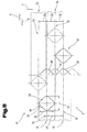
- FIG. 2 shows a schematic diagram of one of the coupling-in units 17, according to FIG. 1.
- a fiber holder 27 for the inlet-side end of the optical fiber 18 is arranged on a frame 26 of the coupling-in unit 17.
- the optical fiber 18 is additionally attached in a socket 28, which can be inserted into the fiber holder 27 and fixed there.
- the fiber holder 27 has at one end a, corresponding to the longitudinal extension of the socket 28 of the optical fiber 18, aligned entrance hatch 29, through which the light of the light sources 14, 15, 16 enters or is coupled into the optical fiber.
- the light sources 14, 15, 16 are each held in a holder or a tube 30, 31, 32 and their light is focused in each case by a lens 33, 34, 35.
- the tubes 30, 31, 32 or optical axes 36, 37, 38 of the lenses 33, 34, 35 are aligned approximately star-shaped.
- the optical axis 38 of the lens 35 is aligned parallel and in alignment with respect to an optical axis 39 of the entrance hatch 29.
- the optical axes 36, 37 of the lenses 33, 34 with respect to the optical axis 39 of the engagement hatch 29 are obliquely aligned and passes the light of the light sources 14, 15 by deflection or reflection at an interference filter 40 or 41 in the entrance hatch 29th the fiber holder 27.
- the optical axes 36, 37 close with the optical axis 39 of the entrance hatch 29 preferably an angle of 60 °. This allows a very compact arrangement of the tubes 30, 31, 32 and the interference filter 40 with respect to the fiber holder 27th
- interference filter 40, 41 for deflecting the beam path of the light sources 14, 15 offers the advantage that light losses can be kept particularly low.
- interference filters are formed by alternating-layer systems, ie multiple layers with alternating high and low refractive indices. Since the layers are virtually free of absorption, a nearly lossless division of a spectral range to reflection and transmission is possible, the limit being determined by a steep edge of the transmission curve.
- a filter is used for the interference filter 40 whose spectral transmittance for red light is almost zero, while light of a smaller wavelength range, such as the green light of the light source 15 and the blue light of the light source 16 Interference filter can pass almost unattenuated.
- the red light of the light source 14 is reflected and passes through the entrance hatch 29 in the optical fiber 18.
- a filter is used as the interference filter 41 whose spectral transmittance for green Light is almost equal to 0, while the blue light of the light source 16 can pass almost lossless through the interference filter 41.
- the green light of the light source 15 is thus reflected to the interference filter 41 and passes through the engagement hatch 29 in the optical fiber 18.
- the peculiarity of the coupling unit 17 is thus that for the deflection of the beam path of the first light source 14 toward the entrance hatch 29 for the Optical fiber 18, an interference filter 40 is used whose spectral transmittance for the wavelength of the light of the light source 14 is almost 0, while the spectral transmittance for the wavelengths of light of the other light sources 15, 16, which must pass through the interference filter 40, almost equal 1 is.
- the second indifference filter 41 on the other hand, has a spectral transmittance which is almost equal to 0 for the wavelength of the light of the second light source 15, while the spectral transmittance of the light of the light source 16 which must pass through this indifference filter 41 is almost equal to 1.
- the light sources 14, 15, 16 in the respective tubes 30, 31, 32 can also be provided that their position with respect to the longitudinal extent of the respective tube 30, 31, 32 can be adjusted. Likewise, the position of the tubes 30, 31, 32 with respect to the frame 26 in the longitudinal extension of the tubes 30, 31, 32 are adjusted. This ensures that the light intensity that reaches the entrance hatch 29 of the fiber holder 27 has the maximum achievable value.
- FIG. 3 shows the exposure head 8 (shown in FIG. 1) arranged above the photosensitive material 2, shown in section.
- the photosensitive material 2 is guided in the region below the exposure head 8 via a table or a plate 42 with a flat upper side. This ensures that the material 2 is aligned parallel to the exit ends of the optical fibers 18.
- the optical fibers 18 guide the light into the exposure head 8.
- the optical fibers 18 each end in a socket 43, which are fastened in a carrier 44.
- the light from the optical fibers 18 is directed by the interposition of a lens system 45 on the photosensitive material 2.
- a mask 47 is arranged with hatches 48 or interposed.
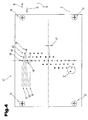
- FIG. 4 shows the mask 47 of the exposure head 8 according to FIG. 3.
- the gaps 48 are distributed in a grid-like manner on the mask 47, so that with respect to a direction perpendicular to the directions 11, 12 of the movement of the exposure head 8 successive gaps 48 are offset by a gap distance d 49.
- a total of 41 gaps 48 are present, so that when moving the exposure head 8 in one of the directions 11, 12 41 lines 40 of pixels on the material 2 can be exposed.
- this is indicated by way of example by the lines 50 shown in the upper area of the mask 47 for the direction of movement 11.
- the image inversion that occurs through the lens system 45 (FIG. 3) should be disregarded in the further description.
- the exit ends 46 of the optical waveguide fibers 18 In order to be able to position the exit ends 46 of the optical waveguide fibers 18 (FIG.
- the hatches 48 are in each case consecutive lines 50, also in the lateral direction, ie with respect to the directions 11, 12 added.
- this lateral displacement of the hatches 48 must be taken into account by a corresponding time delay of the transmission of the data of the digital image 3 to the drive circuit 20 (FIG.
- the mask 47 is preferably formed from a glass sheet provided with a coating. For exact mounting in the exposure head 8, the mask 47 also has centering marks 51.
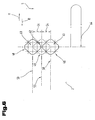
- FIG. 5 shows a greatly enlarged detail of the mask 47 with two hatches 48, according to FIG. 4.
- the illustrated section shows two hatches 48 and dashed lines indicated exposure strips 52, as they are generated by the passage of the hatches 48 in the direction 11 on the photosensitive material 2.
- the exposure head 8 (FIG. 1) over the material 2 only every second line 50 is generated by the lines of the digital image 3 to be generated.
- the generation of corresponding intermediate lines 53 ensues, during a second movement of the exposure head 8, on the basis of the data of the digital image 3.
- successive lines 50, 53 thus have a line spacing z 54 whose value is equal to half the hatch distance d 49.
- This method of applying nested lines 50 and intermediate lines 53 is also referred to as interlacing.
- each hatch 48 perpendicular to the direction 11, 12 of the movement of the exposure head (8) has a height 55 whose value is greater than the line spacing z 54.
- the exposure strips 52 of lines 50 and exposure strips 56 of FIG Intermediate lines 53 between each successive lines 50 and intermediate lines 53 overlap each other. This can be avoided unwanted streaking.
- a width 57 of the hatch 48 has a value which is greater than the line spacing z 54. Both the height 55 and the width 57 of the hatch 48 thus extend beyond the maximum theoretical areal extent of a pixel. This corresponds just to a square with a side length which is equal to the line spacing z 54.
- width 57 of the hatch 48 is consequently also an overlap between adjacent Pixels within a line 50, 53 reached.
- the lateral overlap with respect to the direction 11, 12 is additionally increased by moving the exposure head 8 continuously over the photosensitive material 2 (FIG. 1). This overlap of the exposure areas of individual pixels in the lateral direction 11, 12 results from the path traveled by the exposure head 8 or the hatch 48 during the duration of an exposure pulse.
- the maximum duration of an exposure pulse is equal to the transit time for covering the width of an exposure point corresponding to FIG Line spacing z 54.
- a value between 60% and 95%, in particular 90%, of the propagation time for the width of an exposure point or the transit time for the distance of the line spacing z 54 is preferably selected.
- lateral contours 58, 59 correspond at least approximately to a Gaussian bell curve. Points of material 2 near the maximum width of the hatch 48, i. in an area near the width 57 of the hatch 48, are thus exposed to the exposure of a light pulse much longer than is the case for other points. This is symbolically indicated by exposure curves 60 of the exposure strips 52 and exposure curves 61 of the exposure strips 56, respectively. It is easy to see that in areas where exposure strips 52 and exposure strips 56 overlap one another, the exposure curves 60, 61 overlap, resulting in an overall exposure curve with approximately constant progression and no abrupt changes.
- the height 55 as well as the width 57 of the hatch 48 are preferably equal to 1.8 times the line spacing z 54.
- T difference stands for the time duration between the first exposure process and the second exposure process at the same location of the material 2.
- the method for correcting the intermittency effect thus consists in first producing at least one first line 50 of pixels 53 during a first movement of the exposure head 8 and subsequently producing at least one second line 53 of pixels 62 during a second movement of the exposure head the first row 50 and the second row 53 at least partially overlap each other.
- corrected image data for the second line 53 is calculated by compensating for the changed exposure effect of the second exposure process for each of the pixels 62. This compensation is effected by a change in the intensity and / or by the change in the pulse duration of the corresponding exposure pulse by a value which is proportional to the logarithm of the ratio of the time interval between the exposure of the pixel 63 and the exposure of the pixel 63 and a reference time interval.
- FIG. 6 shows an enlarged section of the photosensitive material 2 with the lines 50 exposed thereon and an intermediate line 53.
- a pixel 62 of the intermediate line 53 and in each case a pixel 63 of the two adjacent rows 50 are indicated by a respective dashed square with the side length corresponding to the value of the line spacing z 54.
- Outlines of the hatches 48 are to be illustrated, the exposure takes place in accordance with the image data of the digital image 3 (FIG. 1), beyond the range of the theoretical maximum areal extent of the pixels 62, 63. The consequence is the overlap of the exposure strips 52, 56 already explained in the description of FIG. 5 (FIG. 5).
- the exposure of the photosensitive material 2 to the lines 50 occurs during movement of the exposure head 8 (FIG. 1) corresponding to the direction 11 (from left to right in FIG. 6).
- the exposure head 8 moves to the right edge of the image until the corresponding lines 50 have been completely exposed.
- the feeding head 8 changes its direction of movement in the direction 12 (from right to left in FIG. 6) and the intermediate line 53 is exposed until, finally, the pixel 62 is exposed at a second point in time.
- the time difference corresponds to a path 64 of the exposure head 8, as can be determined by detecting the position of the exposure head 8 by means of the encoder 24 ( Figure 1) and the speed of movement.
- the delay difference due to the lateral displacement of the hatches 48 would also have to be considered.
- this difference in transit time is negligible in relation to the total runtime.
- FIG. 7 shows a flowchart of the method for exposing digital images 3 with a correction of the intermittency effect.
- a first step 71 the image data is divided into image data corresponding to lines 50 and image data corresponding to intermediate lines 53 (FIGS. 5 and 6), in a further step 72 a recording of the movement sequence of the exposure head 8 and is carried out the advancing movement of the photosensitive material 2 (FIG. 1).
- a step 73 on the basis of this information, time intervals or differential times for adjacent pixels 62, 63 for lines 50 and intermediate lines 53 are determined.
- correction values for the exposure of the intermediate lines 53 are then calculated and thus new corrected image data for the intermediate lines 53 is determined.
- the control of the light sources 14, 15, 16, by the image data to the lines 50 and the intermediate lines 53 are alternately passed to the drive circuit 20.
- the exemplary embodiments show possible embodiments of the device or the method for generating a multicolored image from data of a digital image, it being noted at this point that the invention is not limited to the specifically illustrated embodiments of the same, but rather also various combinations of the individual embodiments are possible with each other and this possibility of variation due to the teaching of technical action by objective invention in the skill of working in this technical field expert. There are therefore also all possible embodiments, which are possible by combinations of individual details of the illustrated and described embodiment, the scope of protection.
Landscapes
- Health & Medical Sciences (AREA)
- General Health & Medical Sciences (AREA)
- Toxicology (AREA)
- Printers Or Recording Devices Using Electromagnetic And Radiation Means (AREA)
- Color, Gradation (AREA)
- Projection-Type Copiers In General (AREA)
- Holo Graphy (AREA)
- Mechanical Optical Scanning Systems (AREA)
Priority Applications (1)
| Application Number | Priority Date | Filing Date | Title |
|---|---|---|---|
| AT05020623T ATE437757T1 (de) | 2004-09-27 | 2005-09-22 | Vorrichtung zum erzeugen eines mehrfarbigen, digitalen bildes |
Applications Claiming Priority (1)
| Application Number | Priority Date | Filing Date | Title |
|---|---|---|---|
| AT0161104A AT500831B1 (de) | 2004-09-27 | 2004-09-27 | Vorrichtung zum erzeugen eines mehrfarbigen, digitalen bildes |
Publications (3)
| Publication Number | Publication Date |
|---|---|
| EP1640169A2 true EP1640169A2 (fr) | 2006-03-29 |
| EP1640169A3 EP1640169A3 (fr) | 2007-10-17 |
| EP1640169B1 EP1640169B1 (fr) | 2009-07-29 |
Family
ID=35636630
Family Applications (1)
| Application Number | Title | Priority Date | Filing Date |
|---|---|---|---|
| EP05020623A Expired - Lifetime EP1640169B1 (fr) | 2004-09-27 | 2005-09-22 | Dispositif pour la production d'images numériques en couleurs multiples |
Country Status (4)
| Country | Link |
|---|---|
| US (1) | US20060066924A1 (fr) |
| EP (1) | EP1640169B1 (fr) |
| AT (3) | AT500831B1 (fr) |
| DE (1) | DE502005007768D1 (fr) |
Cited By (10)
| Publication number | Priority date | Publication date | Assignee | Title |
|---|---|---|---|---|
| EP2471662A1 (fr) * | 2010-12-30 | 2012-07-04 | ALLTEC Angewandte Laserlicht Technologie Gesellschaft mit beschränkter Haftung | Dispositif de surveillance et procédé de surveillance d'éléments de marquage d'une tête de marquage |
| EP2471663A1 (fr) * | 2010-12-30 | 2012-07-04 | ALLTEC Angewandte Laserlicht Technologie Gesellschaft mit beschränkter Haftung | Procédé d'application d'un marquage sur un objet et appareil de marquage |
| EP2471665A1 (fr) * | 2010-12-30 | 2012-07-04 | ALLTEC Angewandte Laserlicht Technologie Gesellschaft mit beschränkter Haftung | Tête de marquage et/ou de balayage, appareil et procédé |
| US8976214B2 (en) | 2010-12-30 | 2015-03-10 | Alltec Angewandte Laserlicht Technologie Gmbh | Device for marking and/or scanning an object |
| US8982335B2 (en) | 2010-12-30 | 2015-03-17 | Alltec Angewandte Laserlicht Technologie Gmbh | Marking or scanning apparatus with a measuring device for measuring the speed of an object and a method of measuring the speed of an object with such a marking or scanning apparatus |
| US9013753B2 (en) | 2010-12-30 | 2015-04-21 | Alltec Angewandte Laserlicht Technologie Gmbh | Apparatus for printing a digital image on an object, apparatus for scanning an object to create a digital image, and related methods of controlling such apparatuses |
| US9041755B2 (en) | 2010-12-30 | 2015-05-26 | Alltec Angewandte Laserlicht Technologie Gmbh | Marking apparatus |
| US9044967B2 (en) | 2010-12-30 | 2015-06-02 | Alltec Angewandte Laserlicht Technologie Gmbh | Marking apparatus and marking method |
| US9132663B2 (en) | 2010-12-30 | 2015-09-15 | Alltec Angewandte Laserlicht Technologie Gmbh | Marking apparatus and method for operating a marking apparatus |
| US9377329B2 (en) | 2010-12-30 | 2016-06-28 | Alltec Angewandte Laserlicht Technologie Gmbh | Sensor apparatus |
Families Citing this family (4)
| Publication number | Priority date | Publication date | Assignee | Title |
|---|---|---|---|---|
| WO2006104171A1 (fr) * | 2005-03-28 | 2006-10-05 | Fujifilm Corporation | Procédé et dispositif d’enregistrement d’image |
| BE1017522A6 (nl) * | 2007-03-21 | 2008-11-04 | Flooring Ind Ltd | Werkwijze voor het vervaardigen van vloerpanelen, alsmede vloerpaneel en halfproduct hierbij verkregen. |
| US8482802B2 (en) * | 2010-03-29 | 2013-07-09 | Eastman Kodak Company | Screened hardcopy reproduction apparatus with compensation |
| BE1019383A3 (nl) | 2010-06-23 | 2012-06-05 | Flooring Ind Ltd Sarl | Werkwijze voor het vervaardigen van panelen en paneel hierbij bekomen. |
Citations (3)
| Publication number | Priority date | Publication date | Assignee | Title |
|---|---|---|---|---|
| EP0072840A1 (fr) | 1981-02-23 | 1983-03-02 | Philips Nv | Procede de multiplexage de voies de transmission au sein d'une fibre optique a saut d'indice et dispositif de mise en oeuvre. |
| US6452696B1 (en) | 1998-05-01 | 2002-09-17 | Zbe Incorporated | Method and apparatus for controlling multiple light sources in a digital printer |
| US20020134909A1 (en) | 1998-07-17 | 2002-09-26 | Akira Shiota | Calibration apparatus for light emitting elements in an optical printer |
Family Cites Families (17)
| Publication number | Priority date | Publication date | Assignee | Title |
|---|---|---|---|---|
| US4540246A (en) * | 1983-03-28 | 1985-09-10 | Polaroid Corporation | Holographic optical apparatus for use with expanded-beam type fiber optical components |
| JP2733055B2 (ja) * | 1986-08-13 | 1998-03-30 | 富士写真フイルム 株式会社 | サイドプリント用ヘツド装置 |
| US4770485A (en) * | 1987-05-05 | 1988-09-13 | Hughes Aircraft Company | Apparatus to launch separated mode groups into optical fibers |
| US4886355A (en) * | 1988-03-28 | 1989-12-12 | Keane Thomas J | Combined gloss and color measuring instrument |
| FR2632404B1 (fr) * | 1988-06-03 | 1990-09-21 | Elf Aquitaine | Capteur interferometrique et son utilisation dans un dispositif interferometrique |
| JPH04110916A (ja) * | 1990-08-31 | 1992-04-13 | Sony Corp | 半導体レーザ用合波装置 |
| JPH0655773A (ja) * | 1992-08-04 | 1994-03-01 | Minolta Camera Co Ltd | 固体走査型プリントヘッド |
| US5535271A (en) * | 1994-05-27 | 1996-07-09 | Hughes Electronics | Apparatus and method for dual tone multifrequency signal detection |
| US6053598A (en) * | 1995-04-13 | 2000-04-25 | Pitney Bowes Inc. | Multiple print head packaging for ink jet printer |
| US5534746A (en) * | 1995-06-06 | 1996-07-09 | Thomson Consumer Electronics, Inc. | Color picture tube having shadow mask with improved aperture spacing |
| ATE300065T1 (de) * | 1998-05-01 | 2005-08-15 | Zbe Inc | Verfahren und gerät zum aufnehmen von digitalen bildern auf fotosensitivem material |
| US6081286A (en) * | 1998-05-02 | 2000-06-27 | Fotland; Richard Allen | Method and apparatus for high speed charge image generation |
| JP3642975B2 (ja) * | 1999-03-30 | 2005-04-27 | フジノン株式会社 | 露光装置 |
| JP2002307742A (ja) * | 2001-04-09 | 2002-10-23 | Hitachi Cable Ltd | Ledプリントヘッド |
| US7006537B2 (en) * | 2001-08-07 | 2006-02-28 | Hrl Laboratories, Llc | Single polarization fiber laser |
| US6636292B2 (en) * | 2001-09-05 | 2003-10-21 | Eastman Kodak Company | Printing apparatus for photosensitive media having a hybrid light source |
| JP2003121923A (ja) * | 2001-10-03 | 2003-04-23 | Lg Electronics Inc | プロジェクタ装置および色合成装置 |
-
2004
- 2004-09-27 AT AT0161104A patent/AT500831B1/de not_active IP Right Cessation
- 2004-09-27 AT ATA698/2007A patent/AT505139B1/de not_active IP Right Cessation
-
2005
- 2005-09-22 EP EP05020623A patent/EP1640169B1/fr not_active Expired - Lifetime
- 2005-09-22 AT AT05020623T patent/ATE437757T1/de not_active IP Right Cessation
- 2005-09-22 DE DE502005007768T patent/DE502005007768D1/de not_active Expired - Fee Related
- 2005-09-26 US US11/234,894 patent/US20060066924A1/en not_active Abandoned
Patent Citations (3)
| Publication number | Priority date | Publication date | Assignee | Title |
|---|---|---|---|---|
| EP0072840A1 (fr) | 1981-02-23 | 1983-03-02 | Philips Nv | Procede de multiplexage de voies de transmission au sein d'une fibre optique a saut d'indice et dispositif de mise en oeuvre. |
| US6452696B1 (en) | 1998-05-01 | 2002-09-17 | Zbe Incorporated | Method and apparatus for controlling multiple light sources in a digital printer |
| US20020134909A1 (en) | 1998-07-17 | 2002-09-26 | Akira Shiota | Calibration apparatus for light emitting elements in an optical printer |
Cited By (23)
| Publication number | Priority date | Publication date | Assignee | Title |
|---|---|---|---|---|
| EP2471662A1 (fr) * | 2010-12-30 | 2012-07-04 | ALLTEC Angewandte Laserlicht Technologie Gesellschaft mit beschränkter Haftung | Dispositif de surveillance et procédé de surveillance d'éléments de marquage d'une tête de marquage |
| EP2471663A1 (fr) * | 2010-12-30 | 2012-07-04 | ALLTEC Angewandte Laserlicht Technologie Gesellschaft mit beschränkter Haftung | Procédé d'application d'un marquage sur un objet et appareil de marquage |
| EP2471665A1 (fr) * | 2010-12-30 | 2012-07-04 | ALLTEC Angewandte Laserlicht Technologie Gesellschaft mit beschränkter Haftung | Tête de marquage et/ou de balayage, appareil et procédé |
| WO2012089325A1 (fr) * | 2010-12-30 | 2012-07-05 | Alltec Angewandte Laserlicht Technologie Gmbh | Tête, appareil et procédé de marquage et/ou d'examen par balayage |
| WO2012089328A1 (fr) * | 2010-12-30 | 2012-07-05 | Alltec Angewandte Laserlicht Technologie Gmbh | Dispositif de contrôle et procédé pour contrôler les éléments de marquage d'une tête de marquage |
| WO2012089321A1 (fr) * | 2010-12-30 | 2012-07-05 | Alltec Angewandte Laserlicht Technologie Gmbh | Procédé permettant d'appliquer un marquage sur un objet et appareil de marquage |
| CN103269863A (zh) * | 2010-12-30 | 2013-08-28 | 奥迪克激光应用技术股份有限公司 | 监控标记头部标记元件的监控设备及方法 |
| US20130271522A1 (en) * | 2010-12-30 | 2013-10-17 | Alltec Angewandte Laserlicht Technologie Gmbh | Monitoring device and method for monitoring marking elements of a marking head |
| US20130286147A1 (en) * | 2010-12-30 | 2013-10-31 | Peter Joerg Kueckendahl | Method for applying a marking on an object and marking apparatus |
| US8976214B2 (en) | 2010-12-30 | 2015-03-10 | Alltec Angewandte Laserlicht Technologie Gmbh | Device for marking and/or scanning an object |
| US8982335B2 (en) | 2010-12-30 | 2015-03-17 | Alltec Angewandte Laserlicht Technologie Gmbh | Marking or scanning apparatus with a measuring device for measuring the speed of an object and a method of measuring the speed of an object with such a marking or scanning apparatus |
| US9007660B2 (en) | 2010-12-30 | 2015-04-14 | Alltec Angewandte Laserlicht Technologie Gmbh | Marking and/or scanning head, apparatus, and method |
| US9013753B2 (en) | 2010-12-30 | 2015-04-21 | Alltec Angewandte Laserlicht Technologie Gmbh | Apparatus for printing a digital image on an object, apparatus for scanning an object to create a digital image, and related methods of controlling such apparatuses |
| US9041755B2 (en) | 2010-12-30 | 2015-05-26 | Alltec Angewandte Laserlicht Technologie Gmbh | Marking apparatus |
| US9044967B2 (en) | 2010-12-30 | 2015-06-02 | Alltec Angewandte Laserlicht Technologie Gmbh | Marking apparatus and marking method |
| US9102168B2 (en) | 2010-12-30 | 2015-08-11 | Alltec Angewandte Laserlicht Technologie Gmbh | Method for applying a marking on an object and marking apparatus |
| US9132663B2 (en) | 2010-12-30 | 2015-09-15 | Alltec Angewandte Laserlicht Technologie Gmbh | Marking apparatus and method for operating a marking apparatus |
| US9145019B2 (en) | 2010-12-30 | 2015-09-29 | Alltec Angewandte Laserlicht Technologie Gmbh | Monitoring device and method for monitoring marking elements of a marking head |
| US9377329B2 (en) | 2010-12-30 | 2016-06-28 | Alltec Angewandte Laserlicht Technologie Gmbh | Sensor apparatus |
| CN103269863B (zh) * | 2010-12-30 | 2016-07-20 | 奥迪克激光应用技术股份有限公司 | 监控标记头部标记元件的监控设备及方法 |
| EA026771B1 (ru) * | 2010-12-30 | 2017-05-31 | Алльтек Ангевандте Лазерлихт Технологи Гмбх | Маркирующая и/или сканирующая головка, маркировочный и/или сканирующий аппарат и способ маркировки и/или сканирования |
| EA028339B1 (ru) * | 2010-12-30 | 2017-11-30 | Алльтек Ангевандте Лазерлихт Технологи Гмбх | Способ нанесения маркировки и маркировочное устройство |
| EA032055B1 (ru) * | 2010-12-30 | 2019-04-30 | Алльтек Ангевандте Лазерлихт Технологи Гмбх | Устройство и способ для контроля маркирующих элементов маркировочной головки |
Also Published As
| Publication number | Publication date |
|---|---|
| US20060066924A1 (en) | 2006-03-30 |
| AT500831B1 (de) | 2008-05-15 |
| EP1640169A3 (fr) | 2007-10-17 |
| ATE437757T1 (de) | 2009-08-15 |
| AT505139B1 (de) | 2012-04-15 |
| EP1640169B1 (fr) | 2009-07-29 |
| DE502005007768D1 (de) | 2009-09-10 |
| AT505139A1 (de) | 2008-11-15 |
| AT500831A1 (de) | 2006-04-15 |
Similar Documents
| Publication | Publication Date | Title |
|---|---|---|
| AT500831B1 (de) | Vorrichtung zum erzeugen eines mehrfarbigen, digitalen bildes | |
| DE3719766C2 (fr) | ||
| DE2539503C3 (de) | Verfahren und Vorrichtung zum Auffinden von Fehlerstellen nicht rechteckiger Form in einer Fotolithografie-Schablone mit Rechteckmuster | |
| DE1921507C2 (de) | Einrichtung zur Erzeugung phasenverschobener elektrischer Signale | |
| DE2535772C2 (de) | Verfahren zum Steuern der Belichtung bei einem photographischen Printer und Vorrichtung zum Durchführen des Verfahrens | |
| DE112014000695T5 (de) | Head-up-Display-Vorrichtung | |
| WO1992008103A1 (fr) | Procede et dispositif pour le mesurage opto-electronique d'objets | |
| EP0847187A2 (fr) | Dispositif de balayage pour la mesure point d'image par point d'image photoélectrique d'un objet à mesurer | |
| DE112019006405T5 (de) | Verfahren zur korrektur eines nichtlinearen abstandsfehlers einer dreidimensionalen abstandsmesskamera mittels pulsphasenverschiebung | |
| DE3232577A1 (de) | Verfahren und vorrichtung zur farbkonzentrationsmessung in druckerzeugnissen | |
| DE3016964C2 (fr) | ||
| DE1165303B (de) | Optisches Bilduebertragungssystem | |
| DE60116206T2 (de) | Optischer Druckkopf eines Randdruckgerätes zum Drucken von Daten auf lichtempfindliches Material | |
| DE102019113267B4 (de) | Verfahren zum Betreiben einer Tintenstrahldruckmaschine mit zumindest einer Modifikationsfunktion | |
| DE3422566C2 (fr) | ||
| DE2654319A1 (de) | Belichtungseinrichtung fuer kopiergeraete | |
| AT516377B1 (de) | Biegevorrichtung mit Messeinrichtung | |
| AT525543B1 (de) | Lichtleiterfaserband und Verfahren zu dessen Herstellung | |
| DE2822639A1 (de) | Einrichtung zur erzeugung fotografischer belichtungen mit hilfe eines digital gespeicherten bildinhaltes und eines relativ zu einem lichtempfindlichen material bewegten reproduktionskopfes | |
| DE2308651C3 (de) | Elektrostatisches Mehrfarbenkopiergerät | |
| DE102022108751A1 (de) | Verfahren zum Betreiben einer Tintenstrahldruckmaschine zum Erzeugen reproduzierbarer Druckergebnisse | |
| CH630184A5 (en) | Film scanner | |
| DE102020129871A1 (de) | Verfahren zum Betreiben einer Tintenstrahldruckmaschine | |
| DE2301393A1 (de) | Verfahren und vorrichtung zum analysieren einer vorlage zur festlegung von rastertonwerten fuer die reproduktion anhand der druckkennlinien einer druckfarbenskala od.dgl | |
| DE3641635A1 (de) | Verfahren und vorrichtung zum steuern der belichtung in drei grundfarben beim farbkopieren |
Legal Events
| Date | Code | Title | Description |
|---|---|---|---|
| PUAI | Public reference made under article 153(3) epc to a published international application that has entered the european phase |
Free format text: ORIGINAL CODE: 0009012 |
|
| AK | Designated contracting states |
Kind code of ref document: A2 Designated state(s): AT BE BG CH CY CZ DE DK EE ES FI FR GB GR HU IE IS IT LI LT LU LV MC NL PL PT RO SE SI SK TR |
|
| AX | Request for extension of the european patent |
Extension state: AL BA HR MK YU |
|
| PUAL | Search report despatched |
Free format text: ORIGINAL CODE: 0009013 |
|
| AK | Designated contracting states |
Kind code of ref document: A3 Designated state(s): AT BE BG CH CY CZ DE DK EE ES FI FR GB GR HU IE IS IT LI LT LU LV MC NL PL PT RO SE SI SK TR |
|
| AX | Request for extension of the european patent |
Extension state: AL BA HR MK YU |
|
| 17P | Request for examination filed |
Effective date: 20080409 |
|
| AKX | Designation fees paid |
Designated state(s): AT BE BG CH CY CZ DE DK EE ES FI FR GB GR HU IE IS IT LI LT LU LV MC NL PL PT RO SE SI SK TR |
|
| AXX | Extension fees paid |
Extension state: YU Payment date: 20080409 Extension state: HR Payment date: 20080409 Extension state: MK Payment date: 20080409 Extension state: AL Payment date: 20080409 Extension state: BA Payment date: 20080409 |
|
| 17Q | First examination report despatched |
Effective date: 20080603 |
|
| GRAP | Despatch of communication of intention to grant a patent |
Free format text: ORIGINAL CODE: EPIDOSNIGR1 |
|
| GRAS | Grant fee paid |
Free format text: ORIGINAL CODE: EPIDOSNIGR3 |
|
| GRAA | (expected) grant |
Free format text: ORIGINAL CODE: 0009210 |
|
| AK | Designated contracting states |
Kind code of ref document: B1 Designated state(s): AT BE BG CH CY CZ DE DK EE ES FI FR GB GR HU IE IS IT LI LT LU LV MC NL PL PT RO SE SI SK TR |
|
| AX | Request for extension of the european patent |
Extension state: AL BA HR MK YU |
|
| REG | Reference to a national code |
Ref country code: GB Ref legal event code: FG4D Free format text: NOT ENGLISH |
|
| REG | Reference to a national code |
Ref country code: CH Ref legal event code: EP |
|
| REG | Reference to a national code |
Ref country code: IE Ref legal event code: FG4D |
|
| REF | Corresponds to: |
Ref document number: 502005007768 Country of ref document: DE Date of ref document: 20090910 Kind code of ref document: P |
|
| NLV1 | Nl: lapsed or annulled due to failure to fulfill the requirements of art. 29p and 29m of the patents act | ||
| PG25 | Lapsed in a contracting state [announced via postgrant information from national office to epo] |
Ref country code: SE Free format text: LAPSE BECAUSE OF FAILURE TO SUBMIT A TRANSLATION OF THE DESCRIPTION OR TO PAY THE FEE WITHIN THE PRESCRIBED TIME-LIMIT Effective date: 20090729 Ref country code: LT Free format text: LAPSE BECAUSE OF FAILURE TO SUBMIT A TRANSLATION OF THE DESCRIPTION OR TO PAY THE FEE WITHIN THE PRESCRIBED TIME-LIMIT Effective date: 20090729 Ref country code: ES Free format text: LAPSE BECAUSE OF FAILURE TO SUBMIT A TRANSLATION OF THE DESCRIPTION OR TO PAY THE FEE WITHIN THE PRESCRIBED TIME-LIMIT Effective date: 20091109 Ref country code: FI Free format text: LAPSE BECAUSE OF FAILURE TO SUBMIT A TRANSLATION OF THE DESCRIPTION OR TO PAY THE FEE WITHIN THE PRESCRIBED TIME-LIMIT Effective date: 20090729 Ref country code: IS Free format text: LAPSE BECAUSE OF FAILURE TO SUBMIT A TRANSLATION OF THE DESCRIPTION OR TO PAY THE FEE WITHIN THE PRESCRIBED TIME-LIMIT Effective date: 20091129 |
|
| PG25 | Lapsed in a contracting state [announced via postgrant information from national office to epo] |
Ref country code: PL Free format text: LAPSE BECAUSE OF FAILURE TO SUBMIT A TRANSLATION OF THE DESCRIPTION OR TO PAY THE FEE WITHIN THE PRESCRIBED TIME-LIMIT Effective date: 20090729 Ref country code: LV Free format text: LAPSE BECAUSE OF FAILURE TO SUBMIT A TRANSLATION OF THE DESCRIPTION OR TO PAY THE FEE WITHIN THE PRESCRIBED TIME-LIMIT Effective date: 20090729 Ref country code: SI Free format text: LAPSE BECAUSE OF FAILURE TO SUBMIT A TRANSLATION OF THE DESCRIPTION OR TO PAY THE FEE WITHIN THE PRESCRIBED TIME-LIMIT Effective date: 20090729 Ref country code: NL Free format text: LAPSE BECAUSE OF FAILURE TO SUBMIT A TRANSLATION OF THE DESCRIPTION OR TO PAY THE FEE WITHIN THE PRESCRIBED TIME-LIMIT Effective date: 20090729 |
|
| REG | Reference to a national code |
Ref country code: IE Ref legal event code: FD4D |
|
| BERE | Be: lapsed |
Owner name: DURST PHOTOTECHNIK A.G. Effective date: 20090930 |
|
| PG25 | Lapsed in a contracting state [announced via postgrant information from national office to epo] |
Ref country code: PT Free format text: LAPSE BECAUSE OF FAILURE TO SUBMIT A TRANSLATION OF THE DESCRIPTION OR TO PAY THE FEE WITHIN THE PRESCRIBED TIME-LIMIT Effective date: 20091129 Ref country code: BG Free format text: LAPSE BECAUSE OF FAILURE TO SUBMIT A TRANSLATION OF THE DESCRIPTION OR TO PAY THE FEE WITHIN THE PRESCRIBED TIME-LIMIT Effective date: 20091029 |
|
| PG25 | Lapsed in a contracting state [announced via postgrant information from national office to epo] |
Ref country code: EE Free format text: LAPSE BECAUSE OF FAILURE TO SUBMIT A TRANSLATION OF THE DESCRIPTION OR TO PAY THE FEE WITHIN THE PRESCRIBED TIME-LIMIT Effective date: 20090729 Ref country code: RO Free format text: LAPSE BECAUSE OF FAILURE TO SUBMIT A TRANSLATION OF THE DESCRIPTION OR TO PAY THE FEE WITHIN THE PRESCRIBED TIME-LIMIT Effective date: 20090729 Ref country code: DK Free format text: LAPSE BECAUSE OF FAILURE TO SUBMIT A TRANSLATION OF THE DESCRIPTION OR TO PAY THE FEE WITHIN THE PRESCRIBED TIME-LIMIT Effective date: 20090729 Ref country code: IE Free format text: LAPSE BECAUSE OF FAILURE TO SUBMIT A TRANSLATION OF THE DESCRIPTION OR TO PAY THE FEE WITHIN THE PRESCRIBED TIME-LIMIT Effective date: 20090729 Ref country code: MC Free format text: LAPSE BECAUSE OF NON-PAYMENT OF DUE FEES Effective date: 20090930 Ref country code: CZ Free format text: LAPSE BECAUSE OF FAILURE TO SUBMIT A TRANSLATION OF THE DESCRIPTION OR TO PAY THE FEE WITHIN THE PRESCRIBED TIME-LIMIT Effective date: 20090729 |
|
| REG | Reference to a national code |
Ref country code: CH Ref legal event code: PL |
|
| PG25 | Lapsed in a contracting state [announced via postgrant information from national office to epo] |
Ref country code: SK Free format text: LAPSE BECAUSE OF FAILURE TO SUBMIT A TRANSLATION OF THE DESCRIPTION OR TO PAY THE FEE WITHIN THE PRESCRIBED TIME-LIMIT Effective date: 20090729 |
|
| PLBE | No opposition filed within time limit |
Free format text: ORIGINAL CODE: 0009261 |
|
| STAA | Information on the status of an ep patent application or granted ep patent |
Free format text: STATUS: NO OPPOSITION FILED WITHIN TIME LIMIT |
|
| REG | Reference to a national code |
Ref country code: FR Ref legal event code: ST Effective date: 20100531 |
|
| 26N | No opposition filed |
Effective date: 20100503 |
|
| PG25 | Lapsed in a contracting state [announced via postgrant information from national office to epo] |
Ref country code: DE Free format text: LAPSE BECAUSE OF NON-PAYMENT OF DUE FEES Effective date: 20100401 Ref country code: FR Free format text: LAPSE BECAUSE OF NON-PAYMENT OF DUE FEES Effective date: 20090930 |
|
| PG25 | Lapsed in a contracting state [announced via postgrant information from national office to epo] |
Ref country code: BE Free format text: LAPSE BECAUSE OF NON-PAYMENT OF DUE FEES Effective date: 20090930 |
|
| PG25 | Lapsed in a contracting state [announced via postgrant information from national office to epo] |
Ref country code: GR Free format text: LAPSE BECAUSE OF FAILURE TO SUBMIT A TRANSLATION OF THE DESCRIPTION OR TO PAY THE FEE WITHIN THE PRESCRIBED TIME-LIMIT Effective date: 20091030 Ref country code: LI Free format text: LAPSE BECAUSE OF NON-PAYMENT OF DUE FEES Effective date: 20090930 Ref country code: CH Free format text: LAPSE BECAUSE OF NON-PAYMENT OF DUE FEES Effective date: 20090930 |
|
| PG25 | Lapsed in a contracting state [announced via postgrant information from national office to epo] |
Ref country code: AT Free format text: LAPSE BECAUSE OF NON-PAYMENT OF DUE FEES Effective date: 20090922 Ref country code: GB Free format text: LAPSE BECAUSE OF NON-PAYMENT OF DUE FEES Effective date: 20091029 |
|
| PG25 | Lapsed in a contracting state [announced via postgrant information from national office to epo] |
Ref country code: IT Free format text: LAPSE BECAUSE OF FAILURE TO SUBMIT A TRANSLATION OF THE DESCRIPTION OR TO PAY THE FEE WITHIN THE PRESCRIBED TIME-LIMIT Effective date: 20090729 |
|
| PG25 | Lapsed in a contracting state [announced via postgrant information from national office to epo] |
Ref country code: LU Free format text: LAPSE BECAUSE OF NON-PAYMENT OF DUE FEES Effective date: 20090922 |
|
| PG25 | Lapsed in a contracting state [announced via postgrant information from national office to epo] |
Ref country code: HU Free format text: LAPSE BECAUSE OF FAILURE TO SUBMIT A TRANSLATION OF THE DESCRIPTION OR TO PAY THE FEE WITHIN THE PRESCRIBED TIME-LIMIT Effective date: 20100130 |
|
| PG25 | Lapsed in a contracting state [announced via postgrant information from national office to epo] |
Ref country code: TR Free format text: LAPSE BECAUSE OF FAILURE TO SUBMIT A TRANSLATION OF THE DESCRIPTION OR TO PAY THE FEE WITHIN THE PRESCRIBED TIME-LIMIT Effective date: 20090729 |
|
| PG25 | Lapsed in a contracting state [announced via postgrant information from national office to epo] |
Ref country code: CY Free format text: LAPSE BECAUSE OF FAILURE TO SUBMIT A TRANSLATION OF THE DESCRIPTION OR TO PAY THE FEE WITHIN THE PRESCRIBED TIME-LIMIT Effective date: 20090729 |