EP1640313A2 - Vorrichtung und Verfahren zum Verringern der wahrgenommenen Farbverschiebung - Google Patents
Vorrichtung und Verfahren zum Verringern der wahrgenommenen Farbverschiebung Download PDFInfo
- Publication number
- EP1640313A2 EP1640313A2 EP05255646A EP05255646A EP1640313A2 EP 1640313 A2 EP1640313 A2 EP 1640313A2 EP 05255646 A EP05255646 A EP 05255646A EP 05255646 A EP05255646 A EP 05255646A EP 1640313 A2 EP1640313 A2 EP 1640313A2
- Authority
- EP
- European Patent Office
- Prior art keywords
- light
- display device
- filter
- modulating
- red
- Prior art date
- Legal status (The legal status is an assumption and is not a legal conclusion. Google has not performed a legal analysis and makes no representation as to the accuracy of the status listed.)
- Granted
Links
Images







Classifications
-
- G—PHYSICS
- G02—OPTICS
- G02F—OPTICAL DEVICES OR ARRANGEMENTS FOR THE CONTROL OF LIGHT BY MODIFICATION OF THE OPTICAL PROPERTIES OF THE MEDIA OF THE ELEMENTS INVOLVED THEREIN; NON-LINEAR OPTICS; FREQUENCY-CHANGING OF LIGHT; OPTICAL LOGIC ELEMENTS; OPTICAL ANALOGUE/DIGITAL CONVERTERS
- G02F1/00—Devices or arrangements for the control of the intensity, colour, phase, polarisation or direction of light arriving from an independent light source, e.g. switching, gating or modulating; Non-linear optics
- G02F1/01—Devices or arrangements for the control of the intensity, colour, phase, polarisation or direction of light arriving from an independent light source, e.g. switching, gating or modulating; Non-linear optics for the control of the intensity, phase, polarisation or colour
- G02F1/21—Devices or arrangements for the control of the intensity, colour, phase, polarisation or direction of light arriving from an independent light source, e.g. switching, gating or modulating; Non-linear optics for the control of the intensity, phase, polarisation or colour by interference
-
- G—PHYSICS
- G02—OPTICS
- G02B—OPTICAL ELEMENTS, SYSTEMS OR APPARATUS
- G02B26/00—Optical devices or arrangements for the control of light using movable or deformable optical elements
- G02B26/001—Optical devices or arrangements for the control of light using movable or deformable optical elements based on interference in an adjustable optical cavity
-
- G—PHYSICS
- G02—OPTICS
- G02B—OPTICAL ELEMENTS, SYSTEMS OR APPARATUS
- G02B5/00—Optical elements other than lenses
- G02B5/20—Filters
Definitions
- the field of the invention relates microelectromechanical systems (MEMS).
- MEMS microelectromechanical systems
- Microelectromechanical systems include micro mechanical elements, actuators, and electronics. Micromechanical elements may be created using deposition, etching, and or other micromachining processes that etch away parts of substrates and/or deposited material layers or that add layers to form electrical and electromechanical devices.
- An interferometric modulator may comprise a pair of conductive plates, one or both of which may be transparent and/or reflective in whole or part and capable of relative motion upon application of an appropriate electrical signal.
- One plate may comprise a stationary layer deposited on a substrate; the other plate may comprise a metallic membrane separated from the stationary layer by an air gap.
- Such devices have a wide range of applications, and it would be beneficial in the art to utilize and/or modify the characteristics of these types of devices so that their features can be exploited in improving existing products and creating new products that have not yet been developed.
- color displays may be fabricated using color display devices such as interferometric modulators that reflect color light.
- color display devices such as interferometric modulators that reflect color light.
- the color of light output from the display device varies with angle of view. This phenomena is referred to herein as "color shift.” What is needed are designs and methods of reducing this color shift.
- Embodiments include display devices configured to reduce perceived color shift.
- One embodiment is a display device including at least one light-modulating element configured to output colored light.
- the light-modulating element includes first and second reflective surfaces. The second surface is movable with respect to the first surface.
- the display device further includes a filter comprising a layer of material that selectively transmits certain visible wavelengths and substantially filters other visible wavelengths when illuminated with white light.
- the filter is positioned to filter light modulated by the light-modulating element.
- the layer of material selectively transmits colored light when illuminated with white light.
- Another embodiment is a method of fabricating a display.
- the method includes forming a light-modulating element configured to output colored light, the color light-modulating element comprising first and second reflective surfaces that form a cavity, the second surface being movable with respect to the first surface.
- the method further includes positioning a filter comprising a layer of material with respect to the light-modulating element such that the filter filters light modulated by the light-modulating element, the layer of material selectively transmitting certain visible wavelengths and substantially filtering other visible wavelengths when illuminated with white light.
- Another embodiment is a display device including at least one light-modulating element configured to output light having at least one spectral peak within the visible spectrum, the light-modulating element comprising first and second reflective surfaces, the second surface being movable with respect to the first surface.
- the display further includes a light emitter that outputs visible light having at least one spectral peak within the visible spectrum, the light emitter configured to illuminate the first and second reflective surfaces of the light-modulating element.
- the light-modulating element is configured to output colored light.
- the light emitter comprises a color light emitter that outputs colored light.
- Another embodiment is a method of fabricating a display device.
- the method includes providing a light-modulating element configured to output light having at least one spectral peak within the visible spectrum, the light-modulating element comprising first and second reflective surfaces, the second surface being movable with respect to the first surface.
- the method further includes positioning a light emitter with respect to the light-modulating element to illuminate the first and second reflective surfaces of the light-modulating element, the light emitter outputting visible light having at least one spectral peak within the visible spectrum.
- Another embodiment is a display device including a plurality of light-modulating elements configured to output colored light, the light-modulating elements comprising first and second reflective surfaces, the second surface being movable with respect to the first surface.
- the display device further includes a filter array comprising a plurality of filter elements that selectively transmit certain visible wavelengths and substantially filters other visible wavelengths when illuminated with white light, at least two of the filter elements having different transmission spectrums, the filter array positioned to filter light modulated by the light-modulating elements.
- Another embodiment is a method of fabricating a display.
- the method includes forming a plurality of light-modulating elements configured to output colored light, the color light-modulating elements comprising first and second reflective surfaces that form a cavity, the second surface being movable with respect to the first surface.
- the method further includes positioning a filter array comprising a plurality of filter elements with respect to the light-modulating elements such that the filter array filters light modulated by the plurality of light-modulating elements, at least two of the filter elements having different transmission spectrums.
- Another embodiment includes a display device comprising means for interferometrically modulating incident light so as to output colored light, and means for selectively transmitting certain visible wavelengths and substantially filtering other visible wavelengths when illuminated with white light.
- the filtering means reduces perceived color shift of the output colored light.
- Another embodiment includes a method of modulating light.
- the method includes interferometrically modulating incident light so as to output colored light.
- the method further includes filtering at least one of said incident and said output light.
- the filtering comprises selectively transmitting certain visible wavelengths and substantially filtering other visible wavelengths when illuminated.
- Another embodiment includes a display device comprising means for interferometrically modulating incident light so as to output light having at least one spectral peak within the visible spectrum, and means for illuminating the modulating means with visible light having at least one spectral peak within the visible spectrum.
- Another embodiment includes a method of modulating light.
- the method includes illuminating a display with visible light having at least one first spectral peak within the visible spectrum.
- the method further includes interferometrically modulating at least a portion of the light so as to output light having at least one second spectral peak within the visible spectrum.
- Various embodiments of display devices have reduced color shift.
- One embodiment is a display device that includes a color light modulator and a color filter.
- a way of reducing color shift for off axis viewing of the modulator is to reduce the intensity of light incident upon the display that would be reflected when viewed off axis and perceived as a color shift.
- a color light source is configured to provide light having a spectral content that lacks wavelengths that would be reflected by the light modulator when viewed off axis and perceived by the viewer as a color shift.
- the following detailed description is directed to certain specific embodiments of the invention. However, the invention can be embodied in a multitude of different ways. In this description, reference is made to the drawings wherein like parts are designated with like numerals throughout. As will be apparent from the following description, the inventionmay be implemented in any device that is configured to display an image, whether in motion (e.g., video) or stationary (e.g., still image), and whether textual or pictorial.
- motion e.g., video
- stationary e.g., still image
- the invention may be implemented in or associated with a variety of electronic devices such as, but not limited to, mobile telephones, wireless devices, personal data assistants (PDAs), hand-held or portable computers, GPS receivers/navigators, cameras, MP3 players, camcorders, game consoles, wrist watches, clocks, calculators, television monitors, flat panel displays, computer monitors, auto displays (e.g., odometer display, etc.), cockpit controls and/or displays, display of camera views (e.g., display of a rear view camera in a vehicle), electronic photographs, electronic billboards or signs, projectors, architectural structures, packaging, and aesthetic structures (e.g., display of images on a piece of jewelry).
- MEMS devices of similar structure to those described herein can also be used in non-display applications such as in electronic switching devices.
- interferometric modulator display embodiment comprising an interferometric MEMS display element is illustrated in Figure 1.
- the pixels are in either a bright or dark state.
- the display element In the bright ("on” or “open") state, the display element reflects a large portion of incident visible light to a user.
- the dark (“off” or “closed”) state When in the dark (“off” or “closed”) state, the display element reflects little incident visible light to the user.
- the light reflectance properties of the "on” and "off” states may be reversed.
- MEMS pixels can be configured to reflect predominantly at selected colors, allowing for a color display in addition to black and white.
- Figure 1 is an isometric view depicting two adjacent pixels in a series of pixels of a visual display, wherein each pixel comprises a MEMS interferometric modulator.
- an interferometric modulator display comprises a row/column array of these interferometric modulators.
- Each interferometric modulator includes a pair of reflective layers positioned at a variable and controllable distance from each other to form a resonant optical cavity with at least one variable dimension.
- one of the reflective layers may be moved between two positions. In the first position, referred to herein as the released state, the movable layer is positioned at a relatively large distance from a fixed partially reflective layer.
- the movable layer In the second position, the movable layer is positioned more closely adjacent to the partially reflective layer. Incident light that reflects from the two layers interferes constructively or destructively depending on the position of the movable reflective layer, producing either an overall reflective or non-reflective state for each pixel.
- the depicted portion of the pixel array in Figure 1 includes two adjacent interferometric modulators 12a and 12b.
- a movable and highly reflective layer 14a is illustrated in a released position at a predetermined distance from a fixed partially reflective layer 16a.
- the movable highly reflective layer 14b is illustrated in an actuated position adjacent to the fixed partially reflective layer 16b.
- the fixed layers 16a, 16b are electrically conductive, partially transparent and partially reflective, and may be fabricated, for example, by depositing one or more layers each of chromium and indium-tin-oxide onto a transparent substrate 20. The layers are patterned into parallel strips, and may form row electrodes in a display device as described further below.
- the movable layers 14a, 14b may be formed as a series of parallel strips of a deposited metal layer or layers (orthogonal to the row electrodes 16a, 16b) deposited on top of posts 18 and an intervening sacrificial material deposited between the posts 18. When the sacrificial material is etched away, the deformable metal layers are separated from the fixed metal layers by a defined air gap 19.
- a highly conductive and reflective material such as aluminum may be used for the deformable layers, and these strips may form column electrodes in a display device.
- the cavity 19 remains between the layers 14a, 16a and the deformable layer is in a mechanically relaxed state as illustrated by the pixel 12a in Figure 1.
- a potential difference is applied to a selected row and column
- the capacitor formed at the intersection of the row and column electrodes at the corresponding pixel becomes charged, and electrostatic forces pull the electrodes together.
- the movable layer is deformed and is forced against the fixed layer (a dielectric material which is not illustrated in this Figure may be deposited on the fixed layer to prevent shorting and control the separation distance) as illustrated by the pixel 12b on the right in Figure 1.
- the behavior is the same regardless of the polarity of the applied potential difference. In this way, row/column actuation that can control the reflective vs. non-reflective pixel states is analogous in many ways to that used in conventional LCD and other display technologies.
- Figures 2 through 5B illustrate one exemplary process and system for using an array of interferometric modulators in a display application.
- Figure 2 is a system block diagram illustrating one embodiment of an electronic device that may incorporate aspects of the invention.
- the electronic device includes a processor 21 which may be any general purpose single- or multi-chip microprocessor such as an ARM, Pentium® , Pentium II® , Pentium III® , Pentium IV® , Pentium® Pro, an 8051, a MIPS® , a Power PC® , an ALPHA® , or any special purpose microprocessor such as a digital signal processor, microcontroller, or a programmable gate array.
- a processor 21 which may be any general purpose single- or multi-chip microprocessor such as an ARM, Pentium® , Pentium II® , Pentium III® , Pentium IV® , Pentium® Pro, an 8051, a MIPS® , a Power PC® , an ALP
- the processor 21 may be configured to execute one or more software modules.
- the processor may be configured to execute one or more software applications, including a web browser, a telephone application, an email program, or any other software application.
- the processor 21 is also configured to communicate with an array controller 22.
- the array controller 22 includes a row driver circuit 24 and a column driver circuit 26 that provide signals to a pixel array 30.
- the cross section of the array illustrated in Figure 1 is shown by the lines 1-1 in Figure 2.
- the row/column actuation protocol may take advantage of a hysteresis property of these devices illustrated in Figure 3. It may require, for example, a 10 volt potential difference to cause a movable layer to deform from the released state to the actuated state. However, when the voltage is reduced from that value, the movable layer maintains its state as the voltage drops back below 10 volts.
- the movable layer does not release completely until the voltage drops below 2 volts.
- the row/column actuation protocol can be designed such that during row strobing, pixels in the strobed row that are to be actuated are exposed to a voltage difference of about 10 volts, and pixels that are to be released are exposed to a voltage difference of close to zero volts.
- each pixel sees a potential difference within the "stability window" of 3-7 volts in this example.
- This feature makes the pixel design illustrated in Figure I stable under the same applied voltage conditions in either an actuated or released pre-existing state. Since each pixel of the interferometric modulator, whether in the actuated or released state, is essentially a capacitor formed by the fixed and moving reflective layers, this stable state can be held at a voltage within the hysteresis window with almost no power dissipation. Essentially no current flows into the pixel if the applied potential is fixed.
- a display frame may be created by asserting the set of column electrodes in accordance with the desired set of actuated pixels in the first row.
- a row pulse is then applied to the row 1 electrode, actuating the pixels corresponding to the asserted column lines.
- the asserted set of column electrodes is then changed to correspond to the desired set of actuated pixels in the second row.
- a pulse is then applied to the row 2 electrode, actuating the appropriate pixels in row 2 in accordance with the asserted column electrodes.
- the row 1 pixels are unaffected by the row 2 pulse, and remain in the state they were set to during the row 1 pulse. This may be repeated for the entire series of rows in a sequential fashion to produce the frame.
- the frames are refreshed and/or updated with new display data by continually repeating this process at some desired number of frames per second.
- protocols for driving row and column electrodes of pixel arrays to produce display frames are also well known and may be used in conjunction with the present invention.
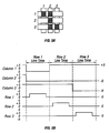
- Figures 4, 5A, and 5B illustrate one possible actuation protocol for creating a display frame on the 3x3 array of Figure 2.
- Figure 4 illustrates a possible set of column and row voltage levels that may be used for pixels exhibiting the hysteresis curves of Figure 3.
- actuating a pixel involves setting the appropriate column to -V bias , and the appropriate row to + ⁇ V, which may correspond to -5 volts and +5 volts respectively Releasing the pixel is accomplished by setting the appropriate column to +V bias , and the appropriate row to the same + ⁇ V, producing a zero volt potential difference across the pixel.
- the pixels are stable in whatever state they were originally in, regardless of whether the column is at +V bias , or -V bias .
- voltages of opposite polarity than those described above can be used, e.g., actuating a pixel can involve setting the appropriate column to +V bias , and the appropriate row to - ⁇ V.
- releasing the pixel is accomplished by setting the appropriate column to -V bias , and the appropriate row to the same - ⁇ V, producing a zero volt potential difference across the pixel.
- Figure 5B is a timing diagram showing a series of row and column signals applied to the 3x3 array of Figure 2 which will result in the display arrangement illustrated in Figure 5A, where actuated pixels are non-reflective.
- the pixels Prior to writing the frame illustrated in Figure 5A, the pixels can be in any state, and in this example, all the rows are at 0 volts, and all the columns are at +5 volts. With these applied voltages, all pixels are stable in their existing actuated or released states.
- pixels (1,1), (1,2), (2,2), (3,2) and (3,3) are actuated.
- columns 1 and 2 are set to-5 volts, and column 3 is set to +5 volts. This does not change the state of any pixels, because all the pixels remain in the 3-7 volt stability window.
- Row 1 is then strobed with a pulse that goes from 0, up to 5 volts, and back to zero. This actuates the (1,1) and (1,2) pixels and releases the (1,3) pixel. No other pixels in the array are affected.
- column 2 is set to -5 volts
- columns 1 and 3 are set to +5 volts.
- Row 3 is similarly set by setting columns 2 and 3 to -5 volts, and column 1 to +5 volts.
- the row 3 strobe sets the row 3 pixels as shown in Figure 5A. After writing the frame, the row potentials are zero, and the column potentials can remain at either +5 or -5 volts, and the display is then stable in the arrangement of Figure 5A. It will be appreciated that the same procedure can be employed for arrays of dozens or hundreds of rows and columns. It will also be appreciated that the timing, sequence, and levels of voltages used to perform row and column actuation can be varied widely within the general principles outlined above, and the above example is exemplary only, and any actuation voltage method can be used with the present invention.
- Figures 6A-6C illustrate three different embodiments of the moving mirror structure.
- Figure 6A is a cross section of the embodiment of Figure 1, where a strip of metal material 14 is deposited on orthogonally extending supports 18.
- the moveable reflective material 14 is attached to supports at the corners only, on tethers 32.
- the moveable reflective material 14 is suspended from a deformable layer 34.
- This embodiment has benefits because the structural design and materials used for the reflective material 14 can be optimized with respect to the optical properties, and the structural design and materials used for the deformable layer 34 can be optimized with respect to desired mechanical properties.
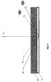
- Figure 7 is a side cross-sectional view of an interferometric modulator 12 illustrating optical paths through the modulator 12.
- the color of light reflected from the interferometric modulator 12 may vary for different angles of incidence (and reflection) with respect to an axis AA as illustrated in Figure 7.
- white light generally refers to light having a sufficiently broad spectral content of approximately uniform intensity as to appear to have no particular color to a viewer.
- Colored light generally refers to light having a sufficiently non-uniform spectral content of visible wavelengths as to appear to have a color to a viewer.
- the interferometric modulator 12 shown in Figure 7 as light travels along the off-axis path A 1 , the light is incident on the interferometric modulator at a first angle, reflects from the interferometric modulator, and travels to a viewer. The viewer perceives a first color when the light reaches the viewer as a result of optical interference between a pair of mirrors in the interferometric modulator 12. When the viewer moves or changes his/her location and thus view angle, the light received by the viewer travels along a different off-axis path A 2 having corresponding a second different angle of incidence (and reflection). Optical interference in the interferometric modulator 12 depends on the optical path length of light propagated within the modulator.
- Different optical path lengths for the different optical paths A 1 and A 2 therefore yield different outputs from the interferometric modulator 12.
- the user therefore perceives different colors depending on his or her angle of view. As described above, this phenomenon is referred to as a "color shift.”
- This color shift is typically identified with reference to a color produced by an interferometric modulator 12 when viewed along the axis AA.
- a reduction in brightness at off-angles may be an acceptable trade-off for reducing the degree of color shift at such off-axis view angles.
- a way of reducing color shift for off axis viewing is to reduce the intensity of light incident upon the display that would be reflected and perceived as color shifted light when viewed off axis. This has the effect of reducing the brightness of the display when viewed off axis relative to viewing normal to the display.
- the perceived color of the interferometric modulator 12 is a function of viewing angle.
- the interferometric modulator 12 merely reflects, rather than generates light, the color of reflected light is dependent on the color of light received by the interferometric modulator 12.
- the degree of color shift of the interferometric modulator 12 observed by off-axis viewing is reduced by filtering light that is incident on the interferometric modulator 12.
- Figure 8 is a side cross-sectional view of the interferometric modulator 12 having a layer 102 of material for selectively transmitting light of a particular color.
- the layer 102 of material may include an absorptive color filter.
- Absorptive filters typically include one or more layers of material that have been doped with a concentration of dye that absorbs particular colors.
- the filter comprises dyed photoresist.
- Exemplary absorptive filter materials are commercially available from several sources, such as International Light, Inc. (Newburyport, MA 01950).
- the layer 102 of material is positioned so as to filter light incident on the interferometric modulator 12 and light reflected by the interferometric modulator 12.
- the layer 102 may be less absorptive of the selected wavelengths of light than would be necessary if light passed through the filter only on the incoming portion of the optical paths of reflected light.
- the layer 102 of material may be positioned with respect to the light modulator so that only light reflected by the modulator passes through the filter.
- a layer of material that forms a light pipe to guide light to illuminate the interferometric modulator 12 may be positioned between the interferometric modulator 12 and the layer 102 of material so that the layer 102 of material only filters light reflected by the interferometric modulator.
- the layer 102 of material may be positioned so as to filter light from an illumination source before that light is incident on the interferometric modulator 12.
- the layer 102 of material may be placed anywhere in the optical path between the source of illumination and the interferometric modulator 12.
- the layer 102 of material may be positioned so that light passes through the layer 102 of material only prior to being reflected by the interferometric modulator 12.
- the layer 102 may be positioned to filter light that is incident light on the interferometric modulator 12, positioned to filter light reflected by the interferometric modulator, or positioned so as to filter incident and reflected light.
- the layer 102 is positioned so as to filter both incident and reflected light.
- the layer 102 may be positioned relative to a light source or the viewer so as to only filter incident light or reflected light from the interferometric modulator 12.
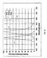
- Figure 9 is a graphical diagram depicting the transmittance of light through an exemplary layer 102 of absorptive material.
- the horizontal axis represents the wavelength of incident light.
- the vertical axis represents the transmittance of light.
- a trace 104 depicts the transmittance of the exemplary layer 102 of material.
- the trace 104 has three transmittance peaks that correspond to wavelength bands associated with primary colors red, green, and blue.
- the spectral response of the layer 102 is selected so that the layer 102 substantially reduces the intensity of the shifted wavelengths of light that would resonate within the interferometric cavity when viewed off axis without substantially reducing the intensity of the wavelengths of light that would be reflected when viewed along or near normal incidence.
- Figure 10 is a graphical diagram in a form similar to Figure 9, which illustrates the spectral response of the interferometric modulator when viewed at two positions, one on-axis, and one off-axis.
- the vertical represents the reflectance of light from the interferometric modulator 12, rather than transmittance as in Figure 9.
- the trace 106 illustrates the on-axis reflectance of the interferometric modulator 12.
- the trace 106 includes a peak in the spectral response in the range of wavelengths associated with red, i.e., the spectral response is of a "red" interferometric modulator 12.
- a trace 110 illustrates the reflectance of the red interferometric modulator 12 at one particular off-axis angle of view.
- the trace 110 includes a peak that is shifted towards the blue portion of the spectrum, e.g., so that the "red" interferometric modulator 12 appears to be orange.
- Figure 11 is a graphical diagram in a form similar to Figure 9, which illustrates the spectral response of the interferometric modulator 12 when viewed at two positions, one on-axis, and one off-axis, through the layer 102 of absorptive material.
- the vertical axis represents the total fraction of light incident on the interferometric modulator that is both reflected by the interferometric modulator 12 and transmitted by the layer 102.
- the traces 104 and 106 which illustrate the spectral response of the layer 102 and the "red" interferometric modulator 12, respectively, are shown with reference to a trace 112 which illustrates the spectral response of reflected light of an embodiment of a display that includes the layer 102 and the "red" interferometric modulator 12.
- the peak in the red end of the visible spectrum of the trace 112 falls sharply between the red and orange portions of the spectrum.
- the red spectral peak of the layer 102 along the trace 104 substantially overlaps the spectral peak of the modulator 12 along the trace 106, e.g., the range of wavelengths over which the peaks extend substantially overlap.
- the spectral response of the interferometric modulator 12 is shifted toward blue (to the left of Figure 11)
- the wavelengths of reflected light that are outside the peak red transmittance band of the layer 102 as illustrated in the trace 104 are filtered out, thus reducing the overall degree of perceived color shift.
- the transmittance of the filter is close to 100% in the portion of the red band that substantially overlaps with the peak of the trace 106, the layer 102 does not substantially reduce the intensity of light reflected by the interferometric modulator when viewed on-axis.
- the display pixels each include one or more red, green, and blue interferometric modulators 12.
- the display includes one or more layers 102 having appropriate transmission peaks in each of red, green, and blue.
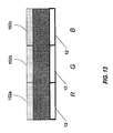
- Figure 12 is a side cross-sectional view of a portion of one embodiment of a color interferometric modulator display, which includes different layers 102a, 102b, and 102c of absorptive material for each of a set of red, green, and blue interferometric modulators 12.
- Each of the layers 102a, 102b, and 102c may include different materials and/or different thicknesses of material or other parameters so that each layer 102a, 102b, and 102c substantially transmits light of only red, green, and blue, respectively.
- the pixel array 30 comprises monochrome pixels, e.g., all of the interferometric modulators 12 in the pixels reflect light having substantially the same spectral content.
- the filter layer 102 selectively transmits the color of the monochrome pixels.
- an interferometric filter is placed between a source of illumination and the interferometric modulator 12 so as to remove wavelengths from the input to the modulator 12 that would be reflected by the modulator 12 and appear to the viewer only when viewed off axis.
- the interferometric modulator 12 may be configured to be illuminated by light having a limited spectral content to reduce perceived off-angle color shift.
- the light source is configured to produce light that does not include the wavelengths of light that appear as shifted light when the modulator 12 is viewed from an off-axis angle of view.
- one embodiment includes red, green, and blue interferometric modulators 12 paired with a light source illuminating the modulators 12 with red, green, and blue light.
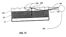
- Figure 13 is a side cross-sectional view of an exemplary display that includes the interferometric modulator 12 and a light source 120.
- the light source 120 illuminates the modulator 12 via a light guide plate 122.
- a light guide 124 is configured to direct light from the light source 120 to the light guide plate 122.
- the light guide plate 122 may include grooves 126 that are formed by angled surfaces 128 from which light 130 may be reflected.
- the light 130 emitted by light source 120 is maintained within the light guide plate 122 by total internal reflection until the light 130 reflects from the surfaces 128, from which it is reflected through the substrate 20 and into the modulator 12.
- any suitable guiding structure may be used.
- the light source 120 is a front light positioned to illuminate the interferometric modulator 12.
- One suitable light source includes one or more color light emitting diodes (LEDs) that have narrow band spectral outputs.
- LEDs are produced by Nichia Corporation, Mountville, PA.
- the light source includes a fluorescent light source, for example, a ultraviolet LED configured to cause suitable phosphors to fluoresce with the desired colors, e.g., red, green, and blue.
- a fluorescent light source for example, a ultraviolet LED configured to cause suitable phosphors to fluoresce with the desired colors, e.g., red, green, and blue.
- Figure 14 is a graphical diagram illustrating the spectral response of an exemplary light source 122.
- the horizontal axis depicts wavelength of emitted light.
- the vertical axis depicts the relative emission intensity of an exemplary light source, such as the Nichia NSTM515AS.
- Traces 130, 132, and 134 illustrate three peaks in the output of the light source at approximately 460, 525, and 630 nm, respectively. These peaks in the traces 130, 132, and 134 correspond to blue, green, and red light.
- Each of the peaks of the exemplary light source has a width at the half maximum of the peak of approximately 50 nm.
- Other light sources may have peaks of different widths, such as between 10-100 nm, or 30-60 nm.
- Figure 15 is a graphical diagram illustrating the spectral response of a display including the interferometric modulator 12 illuminated by the exemplary light source 122 of Figure 14.
- the horizontal axis depicts wavelength of reflected light.
- the vertical axis depicts the reflectivity of light from the interferometric modulators 12.
- the display includes red, green, and blue interferometric modulators.
- traces 140, 142, and 144 illustrate the respective responses of the blue, green, and red interferometric modulators when illuminated by the exemplary light source 122.
- the "blue" trace 140 has a peak centered at 455 nm.
- the "green” trace 142 has a peak centered at 530 nm.
- the "red" trace 144 has a peak centered at 615 nm.
- the display illustrated in Figure 15 is characterized by reduced color shift such as shown in Figure 11 because the light source produces little light for the modulators 12 to reflect when viewed from off-axis angles.
- FIGS 16A and 16B are system block diagrams illustrating an embodiment of a display device 2040.
- the display device 2040 can be, for example, a cellular or mobile telephone.
- the same components of display device 2040 or slight variations thereof are also illustrative of various types of display devices such as televisions and portable media players.
- the display device 2040 includes a housing 2041, a display 2030, an antenna 2043, a speaker 2045, an input device 2048, and a microphone 2046.
- the housing 2041 is generally formed from any of a variety of manufacturing processes as are well known to those of skill in the art, including injection molding, and vacuum forming.
- the housing 2041 may be made from any of a variety of materials, including but not limited to plastic, metal, glass, rubber, and ceramic, or a combination thereof.
- the housing 2041 includes removable portions (not shown) that may be interchanged with other removable portions of different color, or containing different logos, pictures, or symbols.
- the display 2030 of exemplary display device 2040 may be any of a variety of displays, including a bi-stable display, as described herein.
- the display 2030 includes a flat-panel display, such as plasma, EL, OLED, STN LCD, or TFT LCD as described above, or a non-flat-panel display, such as a CRT or other tube device, as is well known to those of skill in the art.
- the display 2030 includes an interferometric modulator display, as described herein.
- the components of one embodiment of exemplary display device 2040 are schematically illustrated in Figure 16B.
- the illustrated exemplary display device 2040 includes a housing 2041 and can include additional components at least partially enclosed therein.
- the exemplary display device 2040 includes a network interface 2027 that includes an antenna 2043 which is coupled to a transceiver 2047.
- the transceiver 2047 is connected to the processor 2021, which is connected to conditioning hardware 2052.
- the conditioning hardware 2052 may be configured to condition a signal (e.g. filter a signal).
- the conditioning hardware 2052 is connected to a speaker 2045 and a microphone 2046.
- the processor 2021 is also connected to an input device 2048 and a driver controller 2029.
- the driver controller 2029 is coupled to a frame buffer 2028 and to the array driver 2022, which in turn is coupled to a display array 2030.
- a power supply 2050 provides power to all components as required by the particular exemplary display device 2040 design.
- the network interface 2027 includes the antenna 2043 and the transceiver 2047 so that the exemplary display device 2040 can communicate with one or more devices over a network. In one embodiment the network interface 2027 may also have some processing capabilities to relieve requirements of the processor 2021.
- the antenna 2043 is any antenna known to those of skill in the art for transmitting and receiving signals. In one embodiment, the antenna transmits and receives RF signals according to the IEEE 802.11 standard, including IEEE 802.11(a), (b), or (g). In another embodiment, the antenna transmits and receives RF signals according to the BLUETOOTH standard. In the case of a cellular telephone, the antenna is designed to receive CDMA, GSM, AMPS or other known signals that are used to communicate within a wireless cell phone network.
- the transceiver 2047 pre-processes the signals received from the antenna 2043 so that they may be received by and further manipulated by the processor 2021.
- the transceiver 2047 also processes signals received from the processor 2021 so that they may be transmitted from the exemplary display device 2040 via the antenna 2043.
- the transceiver 2047 can be replaced by a receiver.
- network interface 2027 can be replaced by an image source, which can store or generate image data to be sent to the processor 2021.
- the image source can be a digital video disc (DVD) or a hard-disc drive that contains image data, or a software module that generates image data.
- Processor 2021 generally controls the overall operation of the exemplary display device 2040.
- the processor 2021 receives data, such as compressed image data from the network interface 2027 or an image source, and processes the data into raw image data or into a format that is readily processed into raw image data.
- the processor 2021 then sends the processed data to the driver controller 2029 or to frame buffer 2028 for storage.
- Raw data typically refers to the information that identifies the image characteristics at each location within an image. For example, such image characteristics can include color, saturation, and gray-scale level.
- the processor 2021 includes a microcontroller, CPU, or logic unit to control operation of the exemplary display device 2040.
- Conditioning hardware 2052 generally includes amplifiers and filters for transmitting signals to the speaker 2045, and for receiving signals from the microphone 2046.
- Conditioning hardware 2052 may be discrete components within the exemplary display device 2040, or may be incorporated within the processor 2021 or other components.
- the driver controller 2029 takes the raw image data generated by the processor 2021 either directly from the processor 2021 or from the frame buffer 2028 and reformats the raw image data appropriately for high speed transmission to the array driver 2022. Specifically, the driver controller 2029 reformats the raw image data into a data flow having a raster-like format, such that it has a time order suitable for scanning across the display array 2030. Then the driver controller 2029 sends the formatted information to the array driver 2022.
- a driver controller 2029 such as a LCD controller, is often associated with the system processor 2021 as a stand-alone Integrated Circuit (IC), such controllers may be implemented in many ways. They may be embedded in the processor 2021 as hardware, embedded in the processor 2021 as software, or fully integrated in hardware with the array driver 2022.
- IC Integrated Circuit
- the array driver 2022 receives the formatted information from the driver controller 2029 and reformats the video data into a parallel set of waveforms that are applied many times per second to the hundreds and sometimes thousands of leads coming from the display's x-y matrix of pixels.
- driver controller 2029, array driver 2022, and display array 2030 are appropriate for any of the types of displays described herein.
- driver controller 2029 is a conventional display controller or a bi-stable display controller (e.g., an interferometric modulator controller).
- array driver 2022 is a conventional driver or a bi-stable display driver (e.g., an interferometric modulator display).
- a driver controller 2029 is integrated with the array driver 2022.
- display array 2030 is a typical display array or a bi-stable display array (e.g., a display including an array of interferometric modulators).
- the input device 2048 allows a user to control the operation of the exemplary display device 2040.
- input device 2048 includes a keypad, such as a QWERTY keyboard or a telephone keypad, a button, a switch, a touch-sensitive screen, a pressure- or heat-sensitive membrane.
- the microphone 2046 is an input device for the exemplary display device 2040. When the microphone 2046 is used to input data to the device, voice commands may be provided by a user for controlling operations of the exemplary display device 2040.
- Power supply 2050 can include a variety of energy storage devices as are well known in the art.
- power supply 2050 is a rechargeable battery, such as a nickel-cadmium battery or a lithium ion battery.
- power supply 2050 is a renewable energy source, a capacitor, or a solar cell, including a plastic solar cell, and solar-cell paint.
- power supply 2050 is configured to receive power from a wall outlet.
- control programmability resides, as described above, in a driver controller which can be located in several places in the electronic display system. In some cases control programmability resides in the array driver 2022. Those of skill in the art will recognize that the above-described optimization may be implemented in any number of hardware and/or software components and in various configurations.
Landscapes
- Physics & Mathematics (AREA)
- General Physics & Mathematics (AREA)
- Optics & Photonics (AREA)
- Spectroscopy & Molecular Physics (AREA)
- Nonlinear Science (AREA)
- Mechanical Light Control Or Optical Switches (AREA)
- Devices For Indicating Variable Information By Combining Individual Elements (AREA)
- Control Of Indicators Other Than Cathode Ray Tubes (AREA)
- Color Television Systems (AREA)
- Spectrometry And Color Measurement (AREA)
Applications Claiming Priority (2)
| Application Number | Priority Date | Filing Date | Title |
|---|---|---|---|
| US61329704P | 2004-09-27 | 2004-09-27 | |
| US11/077,974 US7928928B2 (en) | 2004-09-27 | 2005-03-11 | Apparatus and method for reducing perceived color shift |
Publications (3)
| Publication Number | Publication Date |
|---|---|
| EP1640313A2 true EP1640313A2 (de) | 2006-03-29 |
| EP1640313A3 EP1640313A3 (de) | 2007-03-07 |
| EP1640313B1 EP1640313B1 (de) | 2011-02-02 |
Family
ID=35462336
Family Applications (1)
| Application Number | Title | Priority Date | Filing Date |
|---|---|---|---|
| EP05255646A Expired - Lifetime EP1640313B1 (de) | 2004-09-27 | 2005-09-14 | Vorrichtung und Verfahren zum Verringern der wahrgenommenen Farbverschiebung |
Country Status (14)
| Country | Link |
|---|---|
| US (2) | US7928928B2 (de) |
| EP (1) | EP1640313B1 (de) |
| JP (1) | JP4501075B2 (de) |
| KR (1) | KR20060092910A (de) |
| CN (1) | CN1755491B (de) |
| AT (1) | ATE497479T1 (de) |
| AU (1) | AU2005204551A1 (de) |
| BR (1) | BRPI0503943A (de) |
| CA (1) | CA2519660A1 (de) |
| DE (1) | DE602005026196D1 (de) |
| MX (1) | MXPA05010242A (de) |
| RU (1) | RU2005129951A (de) |
| SG (2) | SG121152A1 (de) |
| TW (1) | TWI447432B (de) |
Cited By (3)
| Publication number | Priority date | Publication date | Assignee | Title |
|---|---|---|---|---|
| EP2312343A1 (de) * | 2009-10-16 | 2011-04-20 | Samsung Corning Precision Materials Co., Ltd. | Optisches Filter für Anzeigegerät und Anzeigegerät mit ebendem |
| US8416154B2 (en) | 2004-09-27 | 2013-04-09 | Qualcomm Mems Technologies, Inc. | Apparatus and method for reducing perceived color shift |
| US9325948B2 (en) | 2012-11-13 | 2016-04-26 | Qualcomm Mems Technologies, Inc. | Real-time compensation for blue shift of electromechanical systems display devices |
Families Citing this family (38)
| Publication number | Priority date | Publication date | Assignee | Title |
|---|---|---|---|---|
| US6674562B1 (en) * | 1994-05-05 | 2004-01-06 | Iridigm Display Corporation | Interferometric modulation of radiation |
| US7907319B2 (en) | 1995-11-06 | 2011-03-15 | Qualcomm Mems Technologies, Inc. | Method and device for modulating light with optical compensation |
| WO1999052006A2 (en) | 1998-04-08 | 1999-10-14 | Etalon, Inc. | Interferometric modulation of radiation |
| US8928967B2 (en) | 1998-04-08 | 2015-01-06 | Qualcomm Mems Technologies, Inc. | Method and device for modulating light |
| TWI289708B (en) | 2002-12-25 | 2007-11-11 | Qualcomm Mems Technologies Inc | Optical interference type color display |
| US7342705B2 (en) | 2004-02-03 | 2008-03-11 | Idc, Llc | Spatial light modulator with integrated optical compensation structure |
| US7855824B2 (en) * | 2004-03-06 | 2010-12-21 | Qualcomm Mems Technologies, Inc. | Method and system for color optimization in a display |
| US7911428B2 (en) | 2004-09-27 | 2011-03-22 | Qualcomm Mems Technologies, Inc. | Method and device for manipulating color in a display |
| US8362987B2 (en) | 2004-09-27 | 2013-01-29 | Qualcomm Mems Technologies, Inc. | Method and device for manipulating color in a display |
| US7898521B2 (en) * | 2004-09-27 | 2011-03-01 | Qualcomm Mems Technologies, Inc. | Device and method for wavelength filtering |
| US7807488B2 (en) * | 2004-09-27 | 2010-10-05 | Qualcomm Mems Technologies, Inc. | Display element having filter material diffused in a substrate of the display element |
| US7813026B2 (en) | 2004-09-27 | 2010-10-12 | Qualcomm Mems Technologies, Inc. | System and method of reducing color shift in a display |
| US20060066557A1 (en) * | 2004-09-27 | 2006-03-30 | Floyd Philip D | Method and device for reflective display with time sequential color illumination |
| US7710632B2 (en) * | 2004-09-27 | 2010-05-04 | Qualcomm Mems Technologies, Inc. | Display device having an array of spatial light modulators with integrated color filters |
| JP2006301043A (ja) * | 2005-04-18 | 2006-11-02 | Agilent Technol Inc | ディスプレイ装置 |
| US7916980B2 (en) | 2006-01-13 | 2011-03-29 | Qualcomm Mems Technologies, Inc. | Interconnect structure for MEMS device |
| US8004743B2 (en) | 2006-04-21 | 2011-08-23 | Qualcomm Mems Technologies, Inc. | Method and apparatus for providing brightness control in an interferometric modulator (IMOD) display |
| EP1943551A2 (de) | 2006-10-06 | 2008-07-16 | Qualcomm Mems Technologies, Inc. | Lichtführung |
| ATE556272T1 (de) | 2006-10-06 | 2012-05-15 | Qualcomm Mems Technologies Inc | Optische verluststruktur in einer beleuchtungsvorrichtung |
| US8068710B2 (en) | 2007-12-07 | 2011-11-29 | Qualcomm Mems Technologies, Inc. | Decoupled holographic film and diffuser |
| WO2009079279A2 (en) * | 2007-12-17 | 2009-06-25 | Qualcomm Mems Technologies, Inc. | Photovoltaics with interferometric back side masks |
| US8654061B2 (en) * | 2008-02-12 | 2014-02-18 | Qualcomm Mems Technologies, Inc. | Integrated front light solution |
| US20100157406A1 (en) * | 2008-12-19 | 2010-06-24 | Qualcomm Mems Technologies, Inc. | System and method for matching light source emission to display element reflectivity |
| WO2010111306A1 (en) * | 2009-03-25 | 2010-09-30 | Qualcomm Mems Technologies, Inc. | Em shielding for display devices |
| WO2010138762A1 (en) * | 2009-05-29 | 2010-12-02 | Qualcomm Mems Technologies, Inc. | Illumination devices for reflective displays |
| WO2010138761A1 (en) | 2009-05-29 | 2010-12-02 | Qualcomm Mems Technologies, Inc. | Illumination devices and methods of fabrication thereof |
| US8848294B2 (en) | 2010-05-20 | 2014-09-30 | Qualcomm Mems Technologies, Inc. | Method and structure capable of changing color saturation |
| CN101907801B (zh) * | 2010-07-23 | 2013-11-27 | 上海交通大学 | 基于可调光学滤波器的平板显示器 |
| US9069421B2 (en) | 2010-12-16 | 2015-06-30 | Hung-Ta LIU | Touch sensor and touch display apparatus and driving method thereof |
| US8941607B2 (en) * | 2010-12-16 | 2015-01-27 | Hung-Ta LIU | MEMS display with touch control function |
| US9046976B2 (en) * | 2011-09-28 | 2015-06-02 | Hung-Ta LIU | Method for transmitting and detecting touch sensing signals and touch device using the same |
| KR102131964B1 (ko) | 2013-10-29 | 2020-07-09 | 삼성디스플레이 주식회사 | 유기 발광 표시 장치 |
| KR102194497B1 (ko) * | 2014-08-14 | 2020-12-24 | 삼성디스플레이 주식회사 | 표시 장치 및 이의 구동 방법 |
| KR101650319B1 (ko) * | 2015-03-06 | 2016-08-24 | 에스엔유 프리시젼 주식회사 | 컬러 카메라를 이용한 두께 측정방법 및 두께 측정장치 |
| US20160313491A1 (en) * | 2015-04-24 | 2016-10-27 | Qualcomm Mems Technologies, Inc. | Illumination structure for use with frontlight |
| CN109219763B (zh) | 2016-06-09 | 2021-03-05 | 3M创新有限公司 | 光学滤光器 |
| TWI706197B (zh) * | 2019-02-01 | 2020-10-01 | 明基材料股份有限公司 | 有機發光二極體顯示器 |
| RU201173U1 (ru) * | 2020-02-26 | 2020-12-01 | Акционерное общество "Научно-производственное объединение автоматики имени академика Н.А. Семихатова" | Переключатель кнопочный с двухцветной светодиодной индикацией |
Citations (1)
| Publication number | Priority date | Publication date | Assignee | Title |
|---|---|---|---|---|
| US20040051929A1 (en) | 1994-05-05 | 2004-03-18 | Sampsell Jeffrey Brian | Separable modulator |
Family Cites Families (211)
| Publication number | Priority date | Publication date | Assignee | Title |
|---|---|---|---|---|
| US2677714A (en) | 1951-09-21 | 1954-05-04 | Alois Vogt Dr | Optical-electrical conversion device comprising a light-permeable metal electrode |
| US3247392A (en) | 1961-05-17 | 1966-04-19 | Optical Coating Laboratory Inc | Optical coating and assembly used as a band pass interference filter reflecting in the ultraviolet and infrared |
| US3448334A (en) * | 1966-09-30 | 1969-06-03 | North American Rockwell | Multicolored e.l. displays using external colored light sources |
| US3653741A (en) * | 1970-02-16 | 1972-04-04 | Alvin M Marks | Electro-optical dipolar material |
| US4389096A (en) * | 1977-12-27 | 1983-06-21 | Matsushita Electric Industrial Co., Ltd. | Image display apparatus of liquid crystal valve projection type |
| US4200472A (en) | 1978-06-05 | 1980-04-29 | The Regents Of The University Of California | Solar power system and high efficiency photovoltaic cells used therein |
| DE3109653A1 (de) | 1980-03-31 | 1982-01-28 | Jenoptik Jena Gmbh, Ddr 6900 Jena | "resonanzabsorber" |
| US4377324A (en) * | 1980-08-04 | 1983-03-22 | Honeywell Inc. | Graded index Fabry-Perot optical filter device |
| US4441791A (en) * | 1980-09-02 | 1984-04-10 | Texas Instruments Incorporated | Deformable mirror light modulator |
| US4400577A (en) | 1981-07-16 | 1983-08-23 | Spear Reginald G | Thin solar cells |
| US4633031A (en) | 1982-09-24 | 1986-12-30 | Todorof William J | Multi-layer thin film, flexible silicon alloy photovoltaic cell |
| US5345322A (en) | 1985-03-01 | 1994-09-06 | Manchester R&D Limited Partnership | Complementary color liquid crystal display |
| US5835255A (en) | 1986-04-23 | 1998-11-10 | Etalon, Inc. | Visible spectrum modulator arrays |
| US4980775A (en) * | 1988-07-21 | 1990-12-25 | Magnascreen Corporation | Modular flat-screen television displays and modules and circuit drives therefor |
| US4982184A (en) * | 1989-01-03 | 1991-01-01 | General Electric Company | Electrocrystallochromic display and element |
| US5192946A (en) * | 1989-02-27 | 1993-03-09 | Texas Instruments Incorporated | Digitized color video display system |
| US5022745A (en) * | 1989-09-07 | 1991-06-11 | Massachusetts Institute Of Technology | Electrostatically deformable single crystal dielectrically coated mirror |
| US5164858A (en) | 1990-03-07 | 1992-11-17 | Deposition Sciences, Inc. | Multi-spectral filter |
| US5225930A (en) * | 1990-05-10 | 1993-07-06 | The United States Of America As Represented By The Secretary Of The Air Force | Comb optical interference filter |
| US5044736A (en) | 1990-11-06 | 1991-09-03 | Motorola, Inc. | Configurable optical filter or display |
| US5233459A (en) | 1991-03-06 | 1993-08-03 | Massachusetts Institute Of Technology | Electric display device |
| US5142414A (en) | 1991-04-22 | 1992-08-25 | Koehler Dale R | Electrically actuatable temporal tristimulus-color device |
| US5287215A (en) * | 1991-07-17 | 1994-02-15 | Optron Systems, Inc. | Membrane light modulation systems |
| US5233385A (en) | 1991-12-18 | 1993-08-03 | Texas Instruments Incorporated | White light enhanced color field sequential projection |
| US5356488A (en) | 1991-12-27 | 1994-10-18 | Rudolf Hezel | Solar cell and method for its manufacture |
| US6381022B1 (en) * | 1992-01-22 | 2002-04-30 | Northeastern University | Light modulating device |
| US5398170A (en) * | 1992-05-18 | 1995-03-14 | Lee; Song S. | Optical-fiber display with intensive brightness |
| JPH06214169A (ja) * | 1992-06-08 | 1994-08-05 | Texas Instr Inc <Ti> | 制御可能な光学的周期的表面フィルタ |
| US5818095A (en) | 1992-08-11 | 1998-10-06 | Texas Instruments Incorporated | High-yield spatial light modulator with light blocking layer |
| US5648860A (en) * | 1992-10-09 | 1997-07-15 | Ag Technology Co., Ltd. | Projection type color liquid crystal optical apparatus |
| JPH06230410A (ja) * | 1993-01-29 | 1994-08-19 | Victor Co Of Japan Ltd | 空間光変調素子 |
| US6674562B1 (en) * | 1994-05-05 | 2004-01-06 | Iridigm Display Corporation | Interferometric modulation of radiation |
| GB2278222A (en) | 1993-05-20 | 1994-11-23 | Sharp Kk | Spatial light modulator |
| US5365283A (en) | 1993-07-19 | 1994-11-15 | Texas Instruments Incorporated | Color phase control for projection display using spatial light modulator |
| US5517347A (en) * | 1993-12-01 | 1996-05-14 | Texas Instruments Incorporated | Direct view deformable mirror device |
| US5448314A (en) | 1994-01-07 | 1995-09-05 | Texas Instruments | Method and apparatus for sequential color imaging |
| DE4407067C2 (de) * | 1994-03-03 | 2003-06-18 | Unaxis Balzers Ag | Dielektrisches Interferenz-Filtersystem, LCD-Anzeige und CCD-Anordnung sowie Verfahren zur Herstellung eines dielektrischen Interferenz-Filtersystems |
| US7138984B1 (en) | 2001-06-05 | 2006-11-21 | Idc, Llc | Directly laminated touch sensitive screen |
| US6040937A (en) * | 1994-05-05 | 2000-03-21 | Etalon, Inc. | Interferometric modulation |
| US6680792B2 (en) * | 1994-05-05 | 2004-01-20 | Iridigm Display Corporation | Interferometric modulation of radiation |
| US7123216B1 (en) | 1994-05-05 | 2006-10-17 | Idc, Llc | Photonic MEMS and structures |
| US20010003487A1 (en) | 1996-11-05 | 2001-06-14 | Mark W. Miles | Visible spectrum modulator arrays |
| US5805117A (en) | 1994-05-12 | 1998-09-08 | Samsung Electronics Co., Ltd. | Large area tiled modular display system |
| KR960705248A (ko) * | 1994-07-15 | 1996-10-09 | 모리시다 요이치 | 헤드업 디스플레이 장치, 액정 디스플레이 패널 및 그 제조방법 |
| US5619059A (en) * | 1994-09-28 | 1997-04-08 | National Research Council Of Canada | Color deformable mirror device having optical thin film interference color coatings |
| US6560018B1 (en) * | 1994-10-27 | 2003-05-06 | Massachusetts Institute Of Technology | Illumination system for transmissive light valve displays |
| JPH08136910A (ja) * | 1994-11-07 | 1996-05-31 | Hitachi Ltd | カラー液晶表示装置およびその製造方法 |
| US5815229A (en) | 1994-11-21 | 1998-09-29 | Proxima Corporation | Microlens imbedded liquid crystal projection panel including thermal insulation layer |
| JP2916887B2 (ja) | 1994-11-29 | 1999-07-05 | キヤノン株式会社 | 電子放出素子、電子源、画像形成装置の製造方法 |
| JP3065494B2 (ja) * | 1994-12-02 | 2000-07-17 | 東芝ライテック株式会社 | 蛍光ランプおよびこれを用いたカラー液晶表示装置 |
| US5886688A (en) | 1995-06-02 | 1999-03-23 | National Semiconductor Corporation | Integrated solar panel and liquid crystal display for portable computer or the like |
| US5835256A (en) | 1995-06-19 | 1998-11-10 | Reflectivity, Inc. | Reflective spatial light modulator with encapsulated micro-mechanical elements |
| US6046840A (en) * | 1995-06-19 | 2000-04-04 | Reflectivity, Inc. | Double substrate reflective spatial light modulator with self-limiting micro-mechanical elements |
| US5739945A (en) * | 1995-09-29 | 1998-04-14 | Tayebati; Parviz | Electrically tunable optical filter utilizing a deformable multi-layer mirror |
| US6324192B1 (en) | 1995-09-29 | 2001-11-27 | Coretek, Inc. | Electrically tunable fabry-perot structure utilizing a deformable multi-layer mirror and method of making the same |
| JP4431196B2 (ja) | 1995-11-06 | 2010-03-10 | アイディーシー エルエルシー | 干渉性変調 |
| US7907319B2 (en) | 1995-11-06 | 2011-03-15 | Qualcomm Mems Technologies, Inc. | Method and device for modulating light with optical compensation |
| US5933183A (en) | 1995-12-12 | 1999-08-03 | Fuji Photo Film Co., Ltd. | Color spatial light modulator and color printer using the same |
| JP3799092B2 (ja) * | 1995-12-29 | 2006-07-19 | アジレント・テクノロジーズ・インク | 光変調装置及びディスプレイ装置 |
| GB2309609A (en) | 1996-01-26 | 1997-07-30 | Sharp Kk | Observer tracking autostereoscopic directional display |
| EP0786911B1 (de) | 1996-01-26 | 2003-09-10 | Sharp Kabushiki Kaisha | Autostereoskopische Anzeigevorrichtung |
| DE19622748A1 (de) | 1996-06-05 | 1997-12-11 | Forschungszentrum Juelich Gmbh | Interferenzfilter auf der Basis von porösem Silicium |
| JP3145309B2 (ja) * | 1996-06-12 | 2001-03-12 | 富士通株式会社 | 平面表示装置及びプラズマディスプレイパネルの近赤外線放出影響防止方法 |
| KR100213968B1 (ko) | 1996-07-15 | 1999-08-02 | 구자홍 | 액정표시장치 |
| US5710656A (en) * | 1996-07-30 | 1998-01-20 | Lucent Technologies Inc. | Micromechanical optical modulator having a reduced-mass composite membrane |
| GB2315902A (en) | 1996-08-01 | 1998-02-11 | Sharp Kk | LIquid crystal device |
| US5868480A (en) * | 1996-12-17 | 1999-02-09 | Compaq Computer Corporation | Image projection apparatus for producing an image supplied by parallel transmitted colored light |
| GB2321532A (en) | 1997-01-22 | 1998-07-29 | Sharp Kk | Multi-colour reflector device and display |
| US5981112A (en) | 1997-01-24 | 1999-11-09 | Eastman Kodak Company | Method of making color filter arrays |
| US6031653A (en) * | 1997-08-28 | 2000-02-29 | California Institute Of Technology | Low-cost thin-metal-film interference filters |
| US6088102A (en) | 1997-10-31 | 2000-07-11 | Silicon Light Machines | Display apparatus including grating light-valve array and interferometric optical system |
| US6285424B1 (en) | 1997-11-07 | 2001-09-04 | Sumitomo Chemical Company, Limited | Black mask, color filter and liquid crystal display |
| US6028690A (en) * | 1997-11-26 | 2000-02-22 | Texas Instruments Incorporated | Reduced micromirror mirror gaps for improved contrast ratio |
| US6492065B2 (en) | 1997-12-05 | 2002-12-10 | Victor Company Of Japan, Limited | Hologram color filter, production method of the same hologram color filter and space light modulating apparatus using the same hologram color filter |
| US5914804A (en) * | 1998-01-28 | 1999-06-22 | Lucent Technologies Inc | Double-cavity micromechanical optical modulator with plural multilayer mirrors |
| US6195196B1 (en) * | 1998-03-13 | 2001-02-27 | Fuji Photo Film Co., Ltd. | Array-type exposing device and flat type display incorporating light modulator and driving method thereof |
| US6967779B2 (en) | 1998-04-15 | 2005-11-22 | Bright View Technologies, Inc. | Micro-lens array with precisely aligned aperture mask and methods of producing same |
| US6282010B1 (en) | 1998-05-14 | 2001-08-28 | Texas Instruments Incorporated | Anti-reflective coatings for spatial light modulators |
| CN100390599C (zh) | 1998-06-05 | 2008-05-28 | 精工爱普生株式会社 | 光源装置和显示装置 |
| CN1129027C (zh) | 1998-06-25 | 2003-11-26 | 时至准钟表股份有限公司 | 反射式彩色液晶显示装置 |
| GB2340281A (en) | 1998-08-04 | 2000-02-16 | Sharp Kk | A reflective liquid crystal display device |
| US6113239A (en) | 1998-09-04 | 2000-09-05 | Sharp Laboratories Of America, Inc. | Projection display system for reflective light valves |
| US6288824B1 (en) | 1998-11-03 | 2001-09-11 | Alex Kastalsky | Display device based on grating electromechanical shutter |
| US6188519B1 (en) | 1999-01-05 | 2001-02-13 | Kenneth Carlisle Johnson | Bigrating light valve |
| JP3657143B2 (ja) | 1999-04-27 | 2005-06-08 | シャープ株式会社 | 太陽電池及びその製造方法 |
| TW477897B (en) | 1999-05-07 | 2002-03-01 | Sharp Kk | Liquid crystal display device, method and device to measure cell thickness of liquid crystal display device, and phase difference plate using the method thereof |
| FI107085B (fi) | 1999-05-28 | 2001-05-31 | Ics Intelligent Control System | Valopaneeli |
| US6201633B1 (en) * | 1999-06-07 | 2001-03-13 | Xerox Corporation | Micro-electromechanical based bistable color display sheets |
| US6597419B1 (en) | 1999-07-02 | 2003-07-22 | Minolta Co., Ltd. | Liquid crystal display including filter means with 10-70% transmittance in the selective reflection wavelength range |
| WO2003007049A1 (en) | 1999-10-05 | 2003-01-23 | Iridigm Display Corporation | Photonic mems and structures |
| US6549338B1 (en) * | 1999-11-12 | 2003-04-15 | Texas Instruments Incorporated | Bandpass filter to reduce thermal impact of dichroic light shift |
| US6466358B2 (en) | 1999-12-30 | 2002-10-15 | Texas Instruments Incorporated | Analog pulse width modulation cell for digital micromechanical device |
| JP2003524215A (ja) * | 2000-02-24 | 2003-08-12 | コーニンクレッカ フィリップス エレクトロニクス エヌ ヴィ | 光導波路を具える表示装置 |
| US6400738B1 (en) * | 2000-04-14 | 2002-06-04 | Agilent Technologies, Inc. | Tunable Fabry-Perot filters and lasers |
| WO2001081994A1 (en) | 2000-04-21 | 2001-11-01 | Seiko Epson Corporation | Electrooptic device, projection type display and method for manufacturing electrooptic device |
| JP2001343514A (ja) | 2000-05-30 | 2001-12-14 | Victor Co Of Japan Ltd | ホログラムカラーフィルタ |
| JP2001345458A (ja) | 2000-05-30 | 2001-12-14 | Kyocera Corp | 太陽電池 |
| JP2001356701A (ja) | 2000-06-15 | 2001-12-26 | Fuji Photo Film Co Ltd | 光学素子、光源ユニットおよび表示装置 |
| US7583335B2 (en) * | 2000-06-27 | 2009-09-01 | Citizen Holdings Co., Ltd. | Liquid crystal display device |
| FR2811139B1 (fr) | 2000-06-29 | 2003-10-17 | Centre Nat Rech Scient | Dispositif optoelectronique a filtrage de longueur d'onde integre |
| US6795605B1 (en) | 2000-08-01 | 2004-09-21 | Cheetah Omni, Llc | Micromechanical optical switch |
| JP2002062505A (ja) | 2000-08-14 | 2002-02-28 | Canon Inc | 投影型表示装置及びそれに用いる干渉性変調素子 |
| US6643069B2 (en) | 2000-08-31 | 2003-11-04 | Texas Instruments Incorporated | SLM-base color projection display having multiple SLM's and multiple projection lenses |
| GB2371119A (en) | 2000-09-25 | 2002-07-17 | Marconi Caswell Ltd | Micro electro-mechanical systems |
| US7072086B2 (en) * | 2001-10-19 | 2006-07-04 | Batchko Robert G | Digital focus lens system |
| US6556338B2 (en) * | 2000-11-03 | 2003-04-29 | Intpax, Inc. | MEMS based variable optical attenuator (MBVOA) |
| JP2002174780A (ja) | 2000-12-08 | 2002-06-21 | Stanley Electric Co Ltd | 反射型カラー表示器 |
| JP2002229023A (ja) | 2001-02-05 | 2002-08-14 | Rohm Co Ltd | カラー液晶表示装置 |
| JP3888075B2 (ja) | 2001-03-23 | 2007-02-28 | セイコーエプソン株式会社 | 光スイッチング素子、光スイッチングデバイス、および画像表示装置 |
| JP2002313121A (ja) | 2001-04-16 | 2002-10-25 | Nitto Denko Corp | タッチパネル付照明装置及び反射型液晶表示装置 |
| JP2002328313A (ja) | 2001-05-01 | 2002-11-15 | Sony Corp | 光スイッチング素子およびその製造方法、並びに画像表示装置 |
| GB2375184A (en) | 2001-05-02 | 2002-11-06 | Marconi Caswell Ltd | Wavelength selectable optical filter |
| JP4526223B2 (ja) | 2001-06-29 | 2010-08-18 | シャープ株式会社 | 配線部材ならびに太陽電池モジュールおよびその製造方法 |
| JP3760810B2 (ja) | 2001-07-06 | 2006-03-29 | ソニー株式会社 | 光変調素子、glvデバイス、及びレーザディスプレイ |
| JP2003021821A (ja) | 2001-07-09 | 2003-01-24 | Toshiba Corp | 液晶ユニットおよびその駆動方法 |
| US6594059B2 (en) * | 2001-07-16 | 2003-07-15 | Axsun Technologies, Inc. | Tilt mirror fabry-perot filter system, fabrication process therefor, and method of operation thereof |
| US6870581B2 (en) * | 2001-10-30 | 2005-03-22 | Sharp Laboratories Of America, Inc. | Single panel color video projection display using reflective banded color falling-raster illumination |
| CN1602451A (zh) * | 2001-11-07 | 2005-03-30 | 应用材料有限公司 | 无掩膜光子电子点格栅阵列光刻机 |
| US7072096B2 (en) * | 2001-12-14 | 2006-07-04 | Digital Optics International, Corporation | Uniform illumination system |
| US6940653B2 (en) | 2001-12-19 | 2005-09-06 | Actuality Systems, Inc. | Radiation conditioning system |
| JP4162900B2 (ja) | 2002-02-05 | 2008-10-08 | アルプス電気株式会社 | 照明装置及び液晶表示装置 |
| JP2003322824A (ja) | 2002-02-26 | 2003-11-14 | Namco Ltd | 立体視映像表示装置および電子機器 |
| US6574033B1 (en) * | 2002-02-27 | 2003-06-03 | Iridigm Display Corporation | Microelectromechanical systems device and method for fabricating same |
| JP2003255338A (ja) | 2002-02-28 | 2003-09-10 | Mitsubishi Electric Corp | 液晶表示装置 |
| US7283112B2 (en) | 2002-03-01 | 2007-10-16 | Microsoft Corporation | Reflective microelectrical mechanical structure (MEMS) optical modulator and optical display system |
| JP2003255344A (ja) | 2002-03-05 | 2003-09-10 | Citizen Electronics Co Ltd | カラー液晶表示装置のフロントライト |
| US6768555B2 (en) | 2002-03-21 | 2004-07-27 | Industrial Technology Research Institute | Fabry-Perot filter apparatus with enhanced optical discrimination |
| US6965468B2 (en) * | 2003-07-03 | 2005-11-15 | Reflectivity, Inc | Micromirror array having reduced gap between adjacent micromirrors of the micromirror array |
| KR20030081662A (ko) | 2002-04-12 | 2003-10-22 | 삼성에스디아이 주식회사 | 이중층 반사방지막이 형성된 태양전지 |
| JP2003307734A (ja) | 2002-04-18 | 2003-10-31 | Brother Ind Ltd | 液晶表示装置及びこれを備えた印刷装置 |
| US6717650B2 (en) | 2002-05-01 | 2004-04-06 | Anvik Corporation | Maskless lithography with sub-pixel resolution |
| KR100433229B1 (ko) | 2002-05-17 | 2004-05-28 | 엘지.필립스 엘시디 주식회사 | 액정표시장치 및 그 제조방법 |
| US6689949B2 (en) | 2002-05-17 | 2004-02-10 | United Innovations, Inc. | Concentrating photovoltaic cavity converters for extreme solar-to-electric conversion efficiencies |
| JP4123415B2 (ja) | 2002-05-20 | 2008-07-23 | ソニー株式会社 | 固体撮像装置 |
| US6741377B2 (en) | 2002-07-02 | 2004-05-25 | Iridigm Display Corporation | Device having a light-absorbing mask and a method for fabricating same |
| US6738194B1 (en) * | 2002-07-22 | 2004-05-18 | The United States Of America As Represented By The Secretary Of The Navy | Resonance tunable optical filter |
| TWI266106B (en) | 2002-08-09 | 2006-11-11 | Sanyo Electric Co | Display device with a plurality of display panels |
| JP4057871B2 (ja) * | 2002-09-19 | 2008-03-05 | 東芝松下ディスプレイテクノロジー株式会社 | 液晶表示装置 |
| JP4440523B2 (ja) * | 2002-09-19 | 2010-03-24 | 大日本印刷株式会社 | インクジェット法による有機el表示装置及びカラーフィルターの製造方法、製造装置 |
| JP2004133430A (ja) | 2002-09-20 | 2004-04-30 | Sony Corp | 表示素子、表示装置、及びマイクロレンズアレイ |
| TW573170B (en) * | 2002-10-11 | 2004-01-21 | Toppoly Optoelectronics Corp | Dual-sided display liquid crystal panel |
| US6747785B2 (en) | 2002-10-24 | 2004-06-08 | Hewlett-Packard Development Company, L.P. | MEMS-actuated color light modulator and methods |
| US7370185B2 (en) | 2003-04-30 | 2008-05-06 | Hewlett-Packard Development Company, L.P. | Self-packaged optical interference display device having anti-stiction bumps, integral micro-lens, and reflection-absorbing layers |
| TWI289708B (en) * | 2002-12-25 | 2007-11-11 | Qualcomm Mems Technologies Inc | Optical interference type color display |
| JP2004205973A (ja) | 2002-12-26 | 2004-07-22 | Fuji Photo Film Co Ltd | 平面表示素子及びその駆動方法 |
| JP2004212673A (ja) | 2002-12-27 | 2004-07-29 | Fuji Photo Film Co Ltd | 平面表示素子及びその駆動方法 |
| TW594155B (en) | 2002-12-27 | 2004-06-21 | Prime View Int Corp Ltd | Optical interference type color display and optical interference modulator |
| JP2004219843A (ja) * | 2003-01-16 | 2004-08-05 | Seiko Epson Corp | 光変調器、表示装置及びその製造方法 |
| US6930816B2 (en) | 2003-01-17 | 2005-08-16 | Fuji Photo Film Co., Ltd. | Spatial light modulator, spatial light modulator array, image forming device and flat panel display |
| TW200413810A (en) * | 2003-01-29 | 2004-08-01 | Prime View Int Co Ltd | Light interference display panel and its manufacturing method |
| TW557395B (en) * | 2003-01-29 | 2003-10-11 | Yen Sun Technology Corp | Optical interference type reflection panel and the manufacturing method thereof |
| TWI226504B (en) * | 2003-04-21 | 2005-01-11 | Prime View Int Co Ltd | A structure of an interference display cell |
| JP3918765B2 (ja) * | 2003-04-21 | 2007-05-23 | セイコーエプソン株式会社 | 液晶表示装置および電子機器 |
| TW567355B (en) * | 2003-04-21 | 2003-12-21 | Prime View Int Co Ltd | An interference display cell and fabrication method thereof |
| US7072093B2 (en) | 2003-04-30 | 2006-07-04 | Hewlett-Packard Development Company, L.P. | Optical interference pixel display with charge control |
| US6811267B1 (en) | 2003-06-09 | 2004-11-02 | Hewlett-Packard Development Company, L.P. | Display system with nonvisible data projection |
| US6822780B1 (en) | 2003-06-23 | 2004-11-23 | Northrop Grumman Corporation | Vertically stacked spatial light modulator with multi-bit phase resolution |
| DE10329917B4 (de) | 2003-07-02 | 2005-12-22 | Schott Ag | Beschichtetes Abdeckglas für Photovoltaik-Module |
| US7190380B2 (en) * | 2003-09-26 | 2007-03-13 | Hewlett-Packard Development Company, L.P. | Generating and displaying spatially offset sub-frames |
| TWI305599B (en) * | 2003-08-15 | 2009-01-21 | Qualcomm Mems Technologies Inc | Interference display panel and method thereof |
| TW200506479A (en) * | 2003-08-15 | 2005-02-16 | Prime View Int Co Ltd | Color changeable pixel for an interference display |
| TW593127B (en) * | 2003-08-18 | 2004-06-21 | Prime View Int Co Ltd | Interference display plate and manufacturing method thereof |
| US20050057442A1 (en) * | 2003-08-28 | 2005-03-17 | Olan Way | Adjacent display of sequential sub-images |
| JP3979982B2 (ja) | 2003-08-29 | 2007-09-19 | シャープ株式会社 | 干渉性変調器および表示装置 |
| WO2005022212A1 (ja) | 2003-09-01 | 2005-03-10 | Dai Nippon Printing Co., Ltd. | プラズマディスプレイ用反射防止フィルム |
| JP2005084331A (ja) * | 2003-09-08 | 2005-03-31 | Fuji Photo Film Co Ltd | 表示装置、画像表示装置および表示方法 |
| US6982820B2 (en) * | 2003-09-26 | 2006-01-03 | Prime View International Co., Ltd. | Color changeable pixel |
| TW200524236A (en) | 2003-12-01 | 2005-07-16 | Nl Nanosemiconductor Gmbh | Optoelectronic device incorporating an interference filter |
| US7161728B2 (en) * | 2003-12-09 | 2007-01-09 | Idc, Llc | Area array modulation and lead reduction in interferometric modulators |
| US7342705B2 (en) * | 2004-02-03 | 2008-03-11 | Idc, Llc | Spatial light modulator with integrated optical compensation structure |
| TW200530669A (en) | 2004-03-05 | 2005-09-16 | Prime View Int Co Ltd | Interference display plate and manufacturing method thereof |
| US7855824B2 (en) | 2004-03-06 | 2010-12-21 | Qualcomm Mems Technologies, Inc. | Method and system for color optimization in a display |
| JP2005308871A (ja) | 2004-04-19 | 2005-11-04 | Aterio Design Kk | 干渉カラーフィルター |
| US7091523B2 (en) * | 2004-05-13 | 2006-08-15 | Eastman Kodak Company | Color OLED device having improved performance |
| US7436389B2 (en) * | 2004-07-29 | 2008-10-14 | Eugene J Mar | Method and system for controlling the output of a diffractive light device |
| US7719500B2 (en) | 2004-09-27 | 2010-05-18 | Qualcomm Mems Technologies, Inc. | Reflective display pixels arranged in non-rectangular arrays |
| US7928928B2 (en) | 2004-09-27 | 2011-04-19 | Qualcomm Mems Technologies, Inc. | Apparatus and method for reducing perceived color shift |
| US7161730B2 (en) * | 2004-09-27 | 2007-01-09 | Idc, Llc | System and method for providing thermal compensation for an interferometric modulator display |
| US8362987B2 (en) * | 2004-09-27 | 2013-01-29 | Qualcomm Mems Technologies, Inc. | Method and device for manipulating color in a display |
| US7679627B2 (en) * | 2004-09-27 | 2010-03-16 | Qualcomm Mems Technologies, Inc. | Controller and driver features for bi-stable display |
| US7750886B2 (en) | 2004-09-27 | 2010-07-06 | Qualcomm Mems Technologies, Inc. | Methods and devices for lighting displays |
| US7807488B2 (en) * | 2004-09-27 | 2010-10-05 | Qualcomm Mems Technologies, Inc. | Display element having filter material diffused in a substrate of the display element |
| US7710632B2 (en) | 2004-09-27 | 2010-05-04 | Qualcomm Mems Technologies, Inc. | Display device having an array of spatial light modulators with integrated color filters |
| US8031133B2 (en) * | 2004-09-27 | 2011-10-04 | Qualcomm Mems Technologies, Inc. | Method and device for manipulating color in a display |
| US7911428B2 (en) * | 2004-09-27 | 2011-03-22 | Qualcomm Mems Technologies, Inc. | Method and device for manipulating color in a display |
| US7304784B2 (en) | 2004-09-27 | 2007-12-04 | Idc, Llc | Reflective display device having viewable display on both sides |
| US7327510B2 (en) * | 2004-09-27 | 2008-02-05 | Idc, Llc | Process for modifying offset voltage characteristics of an interferometric modulator |
| US7898521B2 (en) | 2004-09-27 | 2011-03-01 | Qualcomm Mems Technologies, Inc. | Device and method for wavelength filtering |
| JP4688131B2 (ja) * | 2004-10-21 | 2011-05-25 | 株式会社リコー | 光偏向装置、光偏向アレー、光学システムおよび画像投影表示装置 |
| US20060130889A1 (en) | 2004-12-22 | 2006-06-22 | Motorola, Inc. | Solar panel with optical films |
| US7521666B2 (en) | 2005-02-17 | 2009-04-21 | Capella Microsystems Inc. | Multi-cavity Fabry-Perot ambient light filter apparatus |
| JP2006270021A (ja) | 2005-02-28 | 2006-10-05 | Fuji Photo Film Co Ltd | 積層型光電変換素子 |
| US7771103B2 (en) * | 2005-09-20 | 2010-08-10 | Guardian Industries Corp. | Optical diffuser with IR and/or UV blocking coating |
| US20070115415A1 (en) * | 2005-11-21 | 2007-05-24 | Arthur Piehl | Light absorbers and methods |
| CN102162954A (zh) | 2006-01-24 | 2011-08-24 | 夏普株式会社 | 显示装置、显示装置的制造方法、基板及彩色滤光片基板 |
| US7603001B2 (en) | 2006-02-17 | 2009-10-13 | Qualcomm Mems Technologies, Inc. | Method and apparatus for providing back-lighting in an interferometric modulator display device |
| US7450295B2 (en) | 2006-03-02 | 2008-11-11 | Qualcomm Mems Technologies, Inc. | Methods for producing MEMS with protective coatings using multi-component sacrificial layers |
| US8004743B2 (en) | 2006-04-21 | 2011-08-23 | Qualcomm Mems Technologies, Inc. | Method and apparatus for providing brightness control in an interferometric modulator (IMOD) display |
| JP2009539143A (ja) | 2006-06-01 | 2009-11-12 | ライト レゾナンス テクノロジーズ リミテッド ライアビリティー カンパニー | 光フィルタ/モジュレータ及びフィルタ/モジュレータのアレイ |
| US20080095997A1 (en) * | 2006-10-19 | 2008-04-24 | Tien-Hon Chiang | Function-Enhancing Optical Film |
| JP2008224930A (ja) | 2007-03-12 | 2008-09-25 | Seiko Epson Corp | 表示装置とその製造方法、及び電子機器 |
| US8072402B2 (en) | 2007-08-29 | 2011-12-06 | Qualcomm Mems Technologies, Inc. | Interferometric optical modulator with broadband reflection characteristics |
| KR20100084518A (ko) * | 2007-09-17 | 2010-07-26 | 퀄컴 엠이엠스 테크놀로지스, 인크. | 반투명/반투과반사형 광 간섭계 변조기 장치 |
| US8058549B2 (en) | 2007-10-19 | 2011-11-15 | Qualcomm Mems Technologies, Inc. | Photovoltaic devices with integrated color interferometric film stacks |
| US20090293955A1 (en) | 2007-11-07 | 2009-12-03 | Qualcomm Incorporated | Photovoltaics with interferometric masks |
| WO2009079279A2 (en) | 2007-12-17 | 2009-06-25 | Qualcomm Mems Technologies, Inc. | Photovoltaics with interferometric back side masks |
| US7612933B2 (en) | 2008-03-27 | 2009-11-03 | Qualcomm Mems Technologies, Inc. | Microelectromechanical device with spacing layer |
| US20100096011A1 (en) | 2008-10-16 | 2010-04-22 | Qualcomm Mems Technologies, Inc. | High efficiency interferometric color filters for photovoltaic modules |
| US20100096006A1 (en) | 2008-10-16 | 2010-04-22 | Qualcomm Mems Technologies, Inc. | Monolithic imod color enhanced photovoltaic cell |
| WO2010111306A1 (en) | 2009-03-25 | 2010-09-30 | Qualcomm Mems Technologies, Inc. | Em shielding for display devices |
| US8848294B2 (en) | 2010-05-20 | 2014-09-30 | Qualcomm Mems Technologies, Inc. | Method and structure capable of changing color saturation |
-
2005
- 2005-03-11 US US11/077,974 patent/US7928928B2/en not_active Expired - Fee Related
- 2005-08-31 AU AU2005204551A patent/AU2005204551A1/en not_active Abandoned
- 2005-09-08 JP JP2005260607A patent/JP4501075B2/ja not_active Expired - Fee Related
- 2005-09-09 TW TW094131154A patent/TWI447432B/zh not_active IP Right Cessation
- 2005-09-14 EP EP05255646A patent/EP1640313B1/de not_active Expired - Lifetime
- 2005-09-14 AT AT05255646T patent/ATE497479T1/de not_active IP Right Cessation
- 2005-09-14 DE DE602005026196T patent/DE602005026196D1/de not_active Expired - Lifetime
- 2005-09-15 CA CA002519660A patent/CA2519660A1/en not_active Abandoned
- 2005-09-19 SG SG200506023A patent/SG121152A1/en unknown
- 2005-09-19 SG SG200906383-5A patent/SG155971A1/en unknown
- 2005-09-23 MX MXPA05010242A patent/MXPA05010242A/es not_active Application Discontinuation
- 2005-09-26 RU RU2005129951/28A patent/RU2005129951A/ru not_active Application Discontinuation
- 2005-09-26 BR BRPI0503943-6A patent/BRPI0503943A/pt not_active Application Discontinuation
- 2005-09-26 CN CN2005101050511A patent/CN1755491B/zh not_active Expired - Fee Related
- 2005-09-27 KR KR1020050089754A patent/KR20060092910A/ko not_active Withdrawn
-
2011
- 2011-04-08 US US13/082,904 patent/US8416154B2/en not_active Expired - Fee Related
Patent Citations (1)
| Publication number | Priority date | Publication date | Assignee | Title |
|---|---|---|---|---|
| US20040051929A1 (en) | 1994-05-05 | 2004-03-18 | Sampsell Jeffrey Brian | Separable modulator |
Cited By (3)
| Publication number | Priority date | Publication date | Assignee | Title |
|---|---|---|---|---|
| US8416154B2 (en) | 2004-09-27 | 2013-04-09 | Qualcomm Mems Technologies, Inc. | Apparatus and method for reducing perceived color shift |
| EP2312343A1 (de) * | 2009-10-16 | 2011-04-20 | Samsung Corning Precision Materials Co., Ltd. | Optisches Filter für Anzeigegerät und Anzeigegerät mit ebendem |
| US9325948B2 (en) | 2012-11-13 | 2016-04-26 | Qualcomm Mems Technologies, Inc. | Real-time compensation for blue shift of electromechanical systems display devices |
Also Published As
| Publication number | Publication date |
|---|---|
| ATE497479T1 (de) | 2011-02-15 |
| US20060077122A1 (en) | 2006-04-13 |
| SG121152A1 (en) | 2006-04-26 |
| CA2519660A1 (en) | 2006-03-27 |
| MXPA05010242A (es) | 2006-03-29 |
| DE602005026196D1 (de) | 2011-03-17 |
| TW200622297A (en) | 2006-07-01 |
| US7928928B2 (en) | 2011-04-19 |
| SG155971A1 (en) | 2009-10-29 |
| US8416154B2 (en) | 2013-04-09 |
| KR20060092910A (ko) | 2006-08-23 |
| US20110254849A1 (en) | 2011-10-20 |
| CN1755491B (zh) | 2011-02-02 |
| JP4501075B2 (ja) | 2010-07-14 |
| JP2006113559A (ja) | 2006-04-27 |
| BRPI0503943A (pt) | 2006-05-16 |
| RU2005129951A (ru) | 2007-04-10 |
| AU2005204551A1 (en) | 2006-04-13 |
| EP1640313A3 (de) | 2007-03-07 |
| EP1640313B1 (de) | 2011-02-02 |
| TWI447432B (zh) | 2014-08-01 |
| CN1755491A (zh) | 2006-04-05 |
Similar Documents
| Publication | Publication Date | Title |
|---|---|---|
| EP1640313B1 (de) | Vorrichtung und Verfahren zum Verringern der wahrgenommenen Farbverschiebung | |
| US7911428B2 (en) | Method and device for manipulating color in a display | |
| US8102407B2 (en) | Method and device for manipulating color in a display | |
| US7646529B2 (en) | Method and device for multistate interferometric light modulation | |
| EP1640779A2 (de) | Verfahren und Vorrichtung für Reflexionsvermögen mit einer vorbestimmten spektralen Antwort | |
| EP1640763A1 (de) | Methode und Gerät für mehrstufige interferometrische Lichtmodulation | |
| EP1767981A2 (de) | Verfahren und Vorrichtung zur Farbmanipulation auf einer Anzeige | |
| EP2006714A1 (de) | Infrarotanzeige und Anzeige mit zwei Betriebsarten | |
| EP1640761A1 (de) | Vorrichtung und Verfahren zur Farbmanipulation in einem Display | |
| HK1086634A (en) | Apparatus and method for reducing perceived color shift | |
| HK1087784B (en) | Method and device for multi-state interferometric light modulation |
Legal Events
| Date | Code | Title | Description |
|---|---|---|---|
| PUAI | Public reference made under article 153(3) epc to a published international application that has entered the european phase |
Free format text: ORIGINAL CODE: 0009012 |
|
| AK | Designated contracting states |
Kind code of ref document: A2 Designated state(s): AT BE BG CH CY CZ DE DK EE ES FI FR GB GR HU IE IS IT LI LT LU LV MC NL PL PT RO SE SI SK TR |
|
| AX | Request for extension of the european patent |
Extension state: AL BA HR MK YU |
|
| PUAL | Search report despatched |
Free format text: ORIGINAL CODE: 0009013 |
|
| AK | Designated contracting states |
Kind code of ref document: A3 Designated state(s): AT BE BG CH CY CZ DE DK EE ES FI FR GB GR HU IE IS IT LI LT LU LV MC NL PL PT RO SE SI SK TR |
|
| AX | Request for extension of the european patent |
Extension state: AL BA HR MK YU |
|
| 17P | Request for examination filed |
Effective date: 20070906 |
|
| 17Q | First examination report despatched |
Effective date: 20071012 |
|
| AKX | Designation fees paid |
Designated state(s): AT BE BG CH CY CZ DE DK EE ES FI FR GB GR HU IE IS IT LI LT LU LV MC NL PL PT RO SE SI SK TR |
|
| RAP1 | Party data changed (applicant data changed or rights of an application transferred) |
Owner name: QUALCOMM MEMS TECHNOLOGIES, INC. |
|
| GRAP | Despatch of communication of intention to grant a patent |
Free format text: ORIGINAL CODE: EPIDOSNIGR1 |
|
| GRAS | Grant fee paid |
Free format text: ORIGINAL CODE: EPIDOSNIGR3 |
|
| GRAA | (expected) grant |
Free format text: ORIGINAL CODE: 0009210 |
|
| AK | Designated contracting states |
Kind code of ref document: B1 Designated state(s): AT BE BG CH CY CZ DE DK EE ES FI FR GB GR HU IE IS IT LI LT LU LV MC NL PL PT RO SE SI SK TR |
|
| REG | Reference to a national code |
Ref country code: GB Ref legal event code: FG4D |
|
| REG | Reference to a national code |
Ref country code: CH Ref legal event code: EP |
|
| REG | Reference to a national code |
Ref country code: IE Ref legal event code: FG4D |
|
| REF | Corresponds to: |
Ref document number: 602005026196 Country of ref document: DE Date of ref document: 20110317 Kind code of ref document: P |
|
| REG | Reference to a national code |
Ref country code: DE Ref legal event code: R096 Ref document number: 602005026196 Country of ref document: DE Effective date: 20110317 |
|
| REG | Reference to a national code |
Ref country code: NL Ref legal event code: VDEP Effective date: 20110202 |
|
| LTIE | Lt: invalidation of european patent or patent extension |
Effective date: 20110202 |
|
| PG25 | Lapsed in a contracting state [announced via postgrant information from national office to epo] |
Ref country code: LT Free format text: LAPSE BECAUSE OF FAILURE TO SUBMIT A TRANSLATION OF THE DESCRIPTION OR TO PAY THE FEE WITHIN THE PRESCRIBED TIME-LIMIT Effective date: 20110202 Ref country code: ES Free format text: LAPSE BECAUSE OF FAILURE TO SUBMIT A TRANSLATION OF THE DESCRIPTION OR TO PAY THE FEE WITHIN THE PRESCRIBED TIME-LIMIT Effective date: 20110513 Ref country code: GR Free format text: LAPSE BECAUSE OF FAILURE TO SUBMIT A TRANSLATION OF THE DESCRIPTION OR TO PAY THE FEE WITHIN THE PRESCRIBED TIME-LIMIT Effective date: 20110503 Ref country code: SE Free format text: LAPSE BECAUSE OF FAILURE TO SUBMIT A TRANSLATION OF THE DESCRIPTION OR TO PAY THE FEE WITHIN THE PRESCRIBED TIME-LIMIT Effective date: 20110202 Ref country code: PT Free format text: LAPSE BECAUSE OF FAILURE TO SUBMIT A TRANSLATION OF THE DESCRIPTION OR TO PAY THE FEE WITHIN THE PRESCRIBED TIME-LIMIT Effective date: 20110602 Ref country code: LV Free format text: LAPSE BECAUSE OF FAILURE TO SUBMIT A TRANSLATION OF THE DESCRIPTION OR TO PAY THE FEE WITHIN THE PRESCRIBED TIME-LIMIT Effective date: 20110202 |
|
| PG25 | Lapsed in a contracting state [announced via postgrant information from national office to epo] |
Ref country code: FI Free format text: LAPSE BECAUSE OF FAILURE TO SUBMIT A TRANSLATION OF THE DESCRIPTION OR TO PAY THE FEE WITHIN THE PRESCRIBED TIME-LIMIT Effective date: 20110202 Ref country code: AT Free format text: LAPSE BECAUSE OF FAILURE TO SUBMIT A TRANSLATION OF THE DESCRIPTION OR TO PAY THE FEE WITHIN THE PRESCRIBED TIME-LIMIT Effective date: 20110202 Ref country code: BE Free format text: LAPSE BECAUSE OF FAILURE TO SUBMIT A TRANSLATION OF THE DESCRIPTION OR TO PAY THE FEE WITHIN THE PRESCRIBED TIME-LIMIT Effective date: 20110202 Ref country code: CY Free format text: LAPSE BECAUSE OF FAILURE TO SUBMIT A TRANSLATION OF THE DESCRIPTION OR TO PAY THE FEE WITHIN THE PRESCRIBED TIME-LIMIT Effective date: 20110202 Ref country code: PL Free format text: LAPSE BECAUSE OF FAILURE TO SUBMIT A TRANSLATION OF THE DESCRIPTION OR TO PAY THE FEE WITHIN THE PRESCRIBED TIME-LIMIT Effective date: 20110202 Ref country code: BG Free format text: LAPSE BECAUSE OF FAILURE TO SUBMIT A TRANSLATION OF THE DESCRIPTION OR TO PAY THE FEE WITHIN THE PRESCRIBED TIME-LIMIT Effective date: 20110502 Ref country code: NL Free format text: LAPSE BECAUSE OF FAILURE TO SUBMIT A TRANSLATION OF THE DESCRIPTION OR TO PAY THE FEE WITHIN THE PRESCRIBED TIME-LIMIT Effective date: 20110202 Ref country code: SI Free format text: LAPSE BECAUSE OF FAILURE TO SUBMIT A TRANSLATION OF THE DESCRIPTION OR TO PAY THE FEE WITHIN THE PRESCRIBED TIME-LIMIT Effective date: 20110202 |
|
| PG25 | Lapsed in a contracting state [announced via postgrant information from national office to epo] |
Ref country code: DK Free format text: LAPSE BECAUSE OF FAILURE TO SUBMIT A TRANSLATION OF THE DESCRIPTION OR TO PAY THE FEE WITHIN THE PRESCRIBED TIME-LIMIT Effective date: 20110202 Ref country code: EE Free format text: LAPSE BECAUSE OF FAILURE TO SUBMIT A TRANSLATION OF THE DESCRIPTION OR TO PAY THE FEE WITHIN THE PRESCRIBED TIME-LIMIT Effective date: 20110202 |
|
| PG25 | Lapsed in a contracting state [announced via postgrant information from national office to epo] |
Ref country code: RO Free format text: LAPSE BECAUSE OF FAILURE TO SUBMIT A TRANSLATION OF THE DESCRIPTION OR TO PAY THE FEE WITHIN THE PRESCRIBED TIME-LIMIT Effective date: 20110202 Ref country code: SK Free format text: LAPSE BECAUSE OF FAILURE TO SUBMIT A TRANSLATION OF THE DESCRIPTION OR TO PAY THE FEE WITHIN THE PRESCRIBED TIME-LIMIT Effective date: 20110202 Ref country code: CZ Free format text: LAPSE BECAUSE OF FAILURE TO SUBMIT A TRANSLATION OF THE DESCRIPTION OR TO PAY THE FEE WITHIN THE PRESCRIBED TIME-LIMIT Effective date: 20110202 |
|
| PLBE | No opposition filed within time limit |
Free format text: ORIGINAL CODE: 0009261 |
|
| STAA | Information on the status of an ep patent application or granted ep patent |
Free format text: STATUS: NO OPPOSITION FILED WITHIN TIME LIMIT |
|
| 26N | No opposition filed |
Effective date: 20111103 |
|
| REG | Reference to a national code |
Ref country code: DE Ref legal event code: R097 Ref document number: 602005026196 Country of ref document: DE Effective date: 20111103 |
|
| PG25 | Lapsed in a contracting state [announced via postgrant information from national office to epo] |
Ref country code: MC Free format text: LAPSE BECAUSE OF NON-PAYMENT OF DUE FEES Effective date: 20110930 |
|
| REG | Reference to a national code |
Ref country code: CH Ref legal event code: PL |
|
| PG25 | Lapsed in a contracting state [announced via postgrant information from national office to epo] |
Ref country code: IT Free format text: LAPSE BECAUSE OF FAILURE TO SUBMIT A TRANSLATION OF THE DESCRIPTION OR TO PAY THE FEE WITHIN THE PRESCRIBED TIME-LIMIT Effective date: 20110202 |
|
| REG | Reference to a national code |
Ref country code: IE Ref legal event code: MM4A |
|
| REG | Reference to a national code |
Ref country code: FR Ref legal event code: ST Effective date: 20120531 |
|
| PG25 | Lapsed in a contracting state [announced via postgrant information from national office to epo] |
Ref country code: IE Free format text: LAPSE BECAUSE OF NON-PAYMENT OF DUE FEES Effective date: 20110914 Ref country code: CH Free format text: LAPSE BECAUSE OF NON-PAYMENT OF DUE FEES Effective date: 20110930 Ref country code: LI Free format text: LAPSE BECAUSE OF NON-PAYMENT OF DUE FEES Effective date: 20110930 |
|
| PG25 | Lapsed in a contracting state [announced via postgrant information from national office to epo] |
Ref country code: FR Free format text: LAPSE BECAUSE OF NON-PAYMENT OF DUE FEES Effective date: 20110930 |
|
| PG25 | Lapsed in a contracting state [announced via postgrant information from national office to epo] |
Ref country code: LU Free format text: LAPSE BECAUSE OF NON-PAYMENT OF DUE FEES Effective date: 20110914 |
|
| PG25 | Lapsed in a contracting state [announced via postgrant information from national office to epo] |
Ref country code: IS Free format text: LAPSE BECAUSE OF FAILURE TO SUBMIT A TRANSLATION OF THE DESCRIPTION OR TO PAY THE FEE WITHIN THE PRESCRIBED TIME-LIMIT Effective date: 20110202 |
|
| PG25 | Lapsed in a contracting state [announced via postgrant information from national office to epo] |
Ref country code: TR Free format text: LAPSE BECAUSE OF FAILURE TO SUBMIT A TRANSLATION OF THE DESCRIPTION OR TO PAY THE FEE WITHIN THE PRESCRIBED TIME-LIMIT Effective date: 20110202 |
|
| PG25 | Lapsed in a contracting state [announced via postgrant information from national office to epo] |
Ref country code: HU Free format text: LAPSE BECAUSE OF FAILURE TO SUBMIT A TRANSLATION OF THE DESCRIPTION OR TO PAY THE FEE WITHIN THE PRESCRIBED TIME-LIMIT Effective date: 20110202 |
|
| PGFP | Annual fee paid to national office [announced via postgrant information from national office to epo] |
Ref country code: GB Payment date: 20140826 Year of fee payment: 10 |
|
| PGFP | Annual fee paid to national office [announced via postgrant information from national office to epo] |
Ref country code: DE Payment date: 20140930 Year of fee payment: 10 |
|
| REG | Reference to a national code |
Ref country code: DE Ref legal event code: R119 Ref document number: 602005026196 Country of ref document: DE |
|
| GBPC | Gb: european patent ceased through non-payment of renewal fee |
Effective date: 20150914 |
|
| PG25 | Lapsed in a contracting state [announced via postgrant information from national office to epo] |
Ref country code: GB Free format text: LAPSE BECAUSE OF NON-PAYMENT OF DUE FEES Effective date: 20150914 Ref country code: DE Free format text: LAPSE BECAUSE OF NON-PAYMENT OF DUE FEES Effective date: 20160401 |