EP1640334B1 - Mikroelektromechanisches Bauteil mit integrierter Abdeckung - Google Patents
Mikroelektromechanisches Bauteil mit integrierter Abdeckung Download PDFInfo
- Publication number
- EP1640334B1 EP1640334B1 EP05255976A EP05255976A EP1640334B1 EP 1640334 B1 EP1640334 B1 EP 1640334B1 EP 05255976 A EP05255976 A EP 05255976A EP 05255976 A EP05255976 A EP 05255976A EP 1640334 B1 EP1640334 B1 EP 1640334B1
- Authority
- EP
- European Patent Office
- Prior art keywords
- lid
- cavity
- opening
- movable element
- slide
- Prior art date
- Legal status (The legal status is an assumption and is not a legal conclusion. Google has not performed a legal analysis and makes no representation as to the accuracy of the status listed.)
- Active
Links
Images






Classifications
-
- B—PERFORMING OPERATIONS; TRANSPORTING
- B81—MICROSTRUCTURAL TECHNOLOGY
- B81C—PROCESSES OR APPARATUS SPECIALLY ADAPTED FOR THE MANUFACTURE OR TREATMENT OF MICROSTRUCTURAL DEVICES OR SYSTEMS
- B81C1/00—Manufacture or treatment of devices or systems in or on a substrate
- B81C1/00015—Manufacture or treatment of devices or systems in or on a substrate for manufacturing microsystems
- B81C1/00261—Processes for packaging MEMS devices
- B81C1/00333—Aspects relating to packaging of MEMS devices, not covered by groups B81C1/00269 - B81C1/00325
-
- B—PERFORMING OPERATIONS; TRANSPORTING
- B81—MICROSTRUCTURAL TECHNOLOGY
- B81C—PROCESSES OR APPARATUS SPECIALLY ADAPTED FOR THE MANUFACTURE OR TREATMENT OF MICROSTRUCTURAL DEVICES OR SYSTEMS
- B81C2203/00—Forming microstructural systems
- B81C2203/01—Packaging MEMS
- B81C2203/0136—Growing or depositing of a covering layer
-
- B—PERFORMING OPERATIONS; TRANSPORTING
- B81—MICROSTRUCTURAL TECHNOLOGY
- B81C—PROCESSES OR APPARATUS SPECIALLY ADAPTED FOR THE MANUFACTURE OR TREATMENT OF MICROSTRUCTURAL DEVICES OR SYSTEMS
- B81C2203/00—Forming microstructural systems
- B81C2203/01—Packaging MEMS
- B81C2203/0145—Hermetically sealing an opening in the lid
-
- B—PERFORMING OPERATIONS; TRANSPORTING
- B81—MICROSTRUCTURAL TECHNOLOGY
- B81C—PROCESSES OR APPARATUS SPECIALLY ADAPTED FOR THE MANUFACTURE OR TREATMENT OF MICROSTRUCTURAL DEVICES OR SYSTEMS
- B81C2203/00—Forming microstructural systems
- B81C2203/01—Packaging MEMS
- B81C2203/0163—Reinforcing a cap, e.g. with ribs
Definitions
- the present invention is directed, in general, to integrated circuit structures and, more specifically, to micro-electro-mechanical system structures.
- Micro-electro-mechanical system (MEMS) devices typically include at least one freely movable structure within a recess formed in a substrate and covered by a "lid" or overlying layer.
- the lid includes openings therethrough to allow etchant to be employed in removing a sacrificial material fixing the movable structure in place until the enclosure surrounding the structure is completely formed.
- Such openings if not too large, may be subsequently sealed by sputtering metal into the opening.
- openings through the lid that are too small may not allow sufficient etchant to pass through to etch the structure as desired. Accordingly, the size of the openings and/or the time required to perform an etch through the openings is constrained.
- US, 5,834,332 describes an MEMS component comprising a movable micromechanical functional element arranged in a cavity having a cover layer supported by webs or pillar-like supports.
- WO 95/09366 relates to a micromechanical device formed in a region on a chip, wherein the region is covered by a flat covering supported on pillar-like structures.
- DE 1000555 relates to a micromechanical element formed on a substrate.
- a multilayer cover is provided in order to increase the strength of the cover and allow larger devices to be covered.
- US 5,992,233 describes a microfabricated gyroscope device to measure rotation about an axis perpendicular to the surface of the substrate.
- MEMS micro-electro-mechanical system
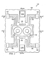
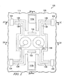
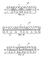
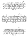
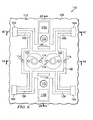
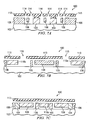
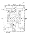
- FIGURES 1 through 8C are diagrams illustrating formation of a micro-electro-mechanical system device structure having an integrated lid supported by pillars and having openings sealed by slides according to one embodiment of the present invention.
- FIGURES 1 through 8C discussed below, and the various embodiments used to describe the principles of the present invention in this patent document are by way of illustration only and should not be construed in any way to limit the scope of the invention. Those skilled in the art will understand that the principles of the present invention may be implemented in any suitably arranged device.
- FIGURES 1 through 8C are diagrams illustrating formation of a micro-electro-mechanical system device structure having an integrated lid supported by pillars and having openings sealed by slides according to one embodiment of the present invention.
- a MEMS device nor the complete process for formation of a MEMS device are depicted or described herein. Instead, for simplicity and clarity, only so much of the structure of a MEMS device and the process for formation of such a device as are unique to the present invention or necessary for an understanding of the present invention are depicted and described.
- FIGURE 1A is a plan view of a partially formed MEMS device structure.
- FIGURES 1A, 1B and 1C are cross-sectional views of the structure depicted in FIGURE 1 taken at section lines A-A, B-B and C-C, respectively.
- the same views of the device structure at different stages of processing are depicted in FIGURES 2 and 2A-2C , 3 and 3A-3C , etc.
- MEMS device structure 100 is formed by patterning recesses 101 in a silicon substrate 102, within which moveable structures will be formed, and leaving elevated regions 103-106.
- a sacrificial oxide material 107 is formed at the bottom of the recesses 101, and polysilicon is deposited thereon and selectively patterned to form movable parts 108, 109 and 110a-110b.
- the structure for the movable parts 108, 109 and 110a-110b is simply patterned from the silicon substrate 102 at the same time that recesses 101 are formed, and extend all the way to the bottom of the recesses 101 in the same manner the elevated regions 103-106.
- the MEMS device structure 100 depicted in the exemplary embodiment is a portion of an accelerometer.
- the accelerometer includes an inertia element or body 108, tethers 109 and anchors 104, where the body 108 and tethers 109 are, at the completion of formation of the MEMS device, freely movable.
- tethers 109 flex to allow movement of body 108 in response to acceleration of the MEMS device structure.
- Body 108 forms a capacitor with one or more other structures, with a capacitance that varies with movement of body 108 in response to acceleration of the integrated circuit containing the MEMS device structure 100.
- anchors 104 are electrically connected to body 108
- electrodes 105 are electrically isolated from body 108. Accordingly, one of body 108 and electrodes 105 may be connected to power and the other connected to ground to work as a variable capacitor.
- the accelerometer body 108 should preferably have a large area and significant mass, but need not necessarily be solid. Accordingly, in the present invention, pillars 103 are formed within openings through the body 108. These pillars 103 will provide support for the integrated lids as described in further detail below. In addition, movable parts 110a and 110b will form slides in the final MEMS device structure that may be moved by applying a voltage to electrodes 105 to seal large openings, also as described in further detail below.
- the grooves between elevated regions 103-106 and movable parts 108, 109 and 110a-110b is backfilled with additional sacrificial oxide 111 as illustrated in the cross-sectional views of FIGURES 2A-2C , with the MEMS device structure 100, covered by the oxide 111, being shown in phantom in the plan view FIGURE 2 .
- the oxide 111 may be conformally deposited, but is then preferably planarized by chemical-mechanical polishing (CMP) or another planarization process. In the example shown, some thickness of oxide 111 remains overlying the tops of elevated regions 103-106 and movable parts 108, 109 and 110a-110b after planarization.
- CMP chemical-mechanical polishing
- openings 112 are etched through the remaining thickness of oxide 111 over pillars 103 as shown in FIGURES 3 and 3A-3C .
- a nitride passivation layer 113 is then formed over the entire structure as depicted in FIGURES 4 and 4A-4C , in contact with the exposed upper surfaces of pillars 103. Nitride 113 will form the integrated lid over the MEMS device structure, supported by pillars 103 in the area over the accelerometer body in the exemplary embodiment.
- small openings 114 through nitride 113 are then formed over the grooves defining the MEMS device structure, while large openings 115, about 3 microns ( ⁇ m) in diameter, are formed through the nitride 113 in the regions adjacent to slides 110a-110b.
- Etchant is then introduced through the openings 114-115, removing the sacrificial oxide 111 as illustrated in FIGURES 6 and 6A-6C .
- a sacrificial oxide 107 was formed under the movable parts, the etchant is also employed to remove that oxide. If no sacrificial oxide 107 was employed, and the movable parts were instead patterned directly from the silicon substrate, a directionally preferential etchant is introduced through openings 114-115 to remove about a 0.5 ⁇ m thickness of silicon at the bottom of the cavities. In either event, this etch should completely undercut the movable parts (body 108, tethers 109 and slides 110a-110b) without completely undercutting the (wider) pillars 103, anchors 104, electrodes 105, and elevated regions 106 as illustrated in FIGURES 7 and 7A-7C .
- the pillars 103 may be formed of the sacrificial oxide material rather than from the substrate, with a width sufficient to prevent the pillars from being completely undercut when the etch is performed to undercut the (narrower) movable parts.
- pillars 103, anchors 104, electrodes 105, and elevated regions 106 should all be wider than the widest portions of body 108, tethers 109 and slides 110a-110b, so that those "fixed" structures are not completely undercut by the directionally preferential etch.
- the thickness of the undercut movable parts is preferably about 3-4 ⁇ m, but may be up to 10-20 ⁇ m.
- Electrodes 105 which may necessitate a hole, not shown, opened through nitride lid 111, or alternatively may be accomplished using conductive structures, also not shown, within the substrate and connected to the bottom of electrodes 105.
- the voltage causes slides 110a-110b to move beneath the large openings as illustrated in FIGURES 8 and 8A-8C .
- Metal or other deposited material is then sputtered to form plugs 116 within the small openings and seals 117 between the slides 110a-110b and nitride lid 111.
- slides 110a-110b are shown as completely disconnected from a remainder of the MEMS device structure 100.
- the slides may in fact be connected by a relatively thin strip of material to a portion of the "frame" (i.e., the elevated regions 106 surrounding the accelerometer) similar to tethers 109, and move beneath the large openings by rotation rather than by translation.
- latches may be formed to retain the slides in place after the slides are moved beneath the opening.
- a ratchet-type pawl-and-catch latch, a pair of detents catching protrusions on biased arms extending from either side of the slide, or any other suitable mechanical latching mechanism may be employed for that purpose.
- the present invention allows MEMS devices having elements with a large but not necessarily continuous area to be formed beneath an integrated lid by providing pillars to support the lid, increasing mechanical strength of the lid against breakage.
- the MEMS device structure is sealed during wafer fabrication without bonding another silicon substrate or ceramic lid over the cavities in which the movable parts are formed.
- the device may be further sealed with a liquid encapsulant prior to singulation.
- the present invention also allows large openings to be formed through the integrated lid to facilitate introduction of the etchant(s) required to separate movable structures from adjacent and/or underlying regions, with slides provided to allow the lid to be sealed against particles and liquids once the MEMS device formation is complete. Larger MEMS devices are possible, since the etchant openings limit the size of structures that may be undercut. Any additional masks required to form the slide and/or additional steps required to, for instance, apply the liquid encapsulant are offset by the processing savings from not using another substrate or a ceramic lid to sealing the MEMS device.
Landscapes
- Engineering & Computer Science (AREA)
- Microelectronics & Electronic Packaging (AREA)
- Manufacturing & Machinery (AREA)
- Micromachines (AREA)
Claims (8)
- Mikroelektromechanischer Vorrichtungsaufbau (100), umfassend:eine Vertiefung (101) innerhalb eines Substrats (102);eine integrierte Abdeckung (113) über der Vertiefung mit einer hindurchgehenden Öffnung (114, 115);ein erstes bewegliches Glied (108), das innerhalb der Vertiefung (102) angeordnet ist, wobei das erste bewegliche Glied eine hindurchgehende Öffnung hat und für die physikalische Bewegung in wenigstens einer Richtung innerhalb der Vertiefung ausgelegt ist; undeine Säule (103), die sich von einem Boden der Vertiefung durch die Öffnung in dem ersten beweglichen Glied (108) zu einer inneren Fläche der integrierten Abdeckung erstreckt; und dadurch gekennzeichnet, dassdie durch die Abdeckung gehende Öffnung (115) durch ein zweites bewegliches Glied (110) innerhalb der Vertiefung (102), das unterhalb der durch die Abdeckung gehenden Öffnung (115) angeordnet ist, und einem Material (117) abgedichtet ist, das zwischen dem zweiten beweglichen Glied und der Abdeckung gebildet ist;wobei das zweite bewegliche Glied (108) derart ausgelegt ist, dass vor der Bildung des Materials (117) zwischen dem zweiten beweglichen Glied und der Abdeckung das zweite bewegliche Glied wahlweise zwischen einer ersten Position innerhalb der Vertiefung (101), in welcher das zweite bewegliche Element nicht unterhalb der durch die Abdeckung gehenden Öffnung (115) angeordnet ist, und einer zweiten Position innerhalb der Vertiefung bewegbar ist, in welcher das zweite bewegliche Glied (110) unterhalb der durch die Abdeckung gehenden Öffnung (115) angeordnet ist.
- Mikroelektromechanischer Vorrichtungsaufbau (100) nach einem der vorhergehenden Ansprüche, bei welchem die Säule (103) eine Breite aufweist, die größer als ein breitester Bereich des bewegenden Teiles oder des ersten beweglichen Gliedes (108) ist.
- Mikroelektromechanischer Vorrichtungsaufbau (100) nach einem der vorhergehenden Ansprüche, bei welchem das zweite bewegliche Glied (110) an eine Seitenwand der Vertiefung angebunden ist.
- Mikroelektromechanischer Vorrichtungsaufbau (100) nach einem der vorhergehenden Ansprüche, bei welchem das zweite bewegliche Glied (110) in einer Position unterhalb der durch die Abdeckung gehenden Öffnung (115) durch wenigstens eine Verrieglung gesichert ist.
- Mikroelektromechanischer Vorrichtungsaufbau (100) nach einem der vorhergehenden Ansprüche, weiter umfassend:ein Opfermaterial (111) innerhalb der Vertiefung zwischen dem ersten beweglichen Glied (108) und wenigstens den Seitenwände der Vertiefung, dem Boden der Vertiefung oder der Abdeckung, wobei der bewegliche Teil derart ausgelegt ist, dass er zu einer physikalischen Bewegung in die wenigstens eine Richtung innerhalb der Vertiefung nach Entfernen des Opfermaterials (111) fähig ist und eines beliebigen anderen Opfermaterials innerhalb der Vertiefung benachbart zu dem bewegenden Teil.
- Verfahren zum Bilden eines Mikroelektromechanischen Vorrichtungsaufbaus (100), wobei das Verfahren umfasst:Bilden einer Vertiefung (101) innerhalb eines Substrats (102);Bilden eines Opfermaterials (111) innerhalb der Vertiefung;Bilder einer integrierten Abdeckung (113) über der Vertiefung, wobei die Abdeckung eine hindurchgehende Öffnung (115) aufweist;Bilden eines Gleiters (110) innerhalb der Vertiefung, der unterhalb der durch die Abdeckung gehenden Öffnung angeordnet ist; und gekennzeichnet durch:wobei vor der Bildung des Materials (117) zwischen dem Gleiter und der Abdeckung der Gleiter (110) wahlweise zwischen einer ersten Position innerhalb der Vertiefung, in welcher der Gleiter nicht unterhalb der durch die Abdeckung gehenden Öffnung angeordnet ist, und einer zweiten Position innerhalb der Vertiefung bewegbar ist, in welcher der Gleiter unterhalb der durch die Abdeckung gehenden Öffnung angeordnet ist.Bilden, nach Entfernen des Opfermaterials aus dem Inneren der Vertiefung, eines Materials (117) zwischen dem Gleiter (110) und der Abdeckung (113), wobei die durch die Abdeckung gehende Öffnung (115) durch den Gleiter und das Material, das zwischen dem Gleiter und der Abdeckung gebildet ist, abgedichtet wird,
- Verfahren nach Anspruch 6, bei welchem der Gleiter (110) an einer Seitenwand der Vertiefung angebunden ist.
- Verfahren nach Anspruch 6 oder 7, bei welchem der Gleiter in der Position unterhalb der durch die Abdeckung gehenden Öffnung durch wenigstens eine Verriegelung gesichert ist.
Applications Claiming Priority (1)
| Application Number | Priority Date | Filing Date | Title |
|---|---|---|---|
| US10/952,183 US7098065B2 (en) | 2004-09-28 | 2004-09-28 | Integrated lid formed on MEMS device |
Publications (3)
| Publication Number | Publication Date |
|---|---|
| EP1640334A2 EP1640334A2 (de) | 2006-03-29 |
| EP1640334A3 EP1640334A3 (de) | 2006-05-17 |
| EP1640334B1 true EP1640334B1 (de) | 2009-11-25 |
Family
ID=35623700
Family Applications (1)
| Application Number | Title | Priority Date | Filing Date |
|---|---|---|---|
| EP05255976A Active EP1640334B1 (de) | 2004-09-28 | 2005-09-26 | Mikroelektromechanisches Bauteil mit integrierter Abdeckung |
Country Status (3)
| Country | Link |
|---|---|
| US (1) | US7098065B2 (de) |
| EP (1) | EP1640334B1 (de) |
| DE (1) | DE602005017858D1 (de) |
Families Citing this family (8)
| Publication number | Priority date | Publication date | Assignee | Title |
|---|---|---|---|---|
| US7585744B2 (en) * | 2003-12-08 | 2009-09-08 | Freescale Semiconductor, Inc. | Method of forming a seal for a semiconductor device |
| JP4726927B2 (ja) * | 2008-06-19 | 2011-07-20 | 株式会社日立製作所 | 集積化マイクロエレクトロメカニカルシステムおよびその製造方法 |
| WO2010006065A2 (en) * | 2008-07-08 | 2010-01-14 | Wispry, Inc. | Thin-film lid mems devices and methods |
| US8877648B2 (en) * | 2009-03-26 | 2014-11-04 | Semprius, Inc. | Methods of forming printable integrated circuit devices by selective etching to suspend the devices from a handling substrate and devices formed thereby |
| EP2697155B1 (de) | 2011-04-14 | 2017-01-11 | Robert Bosch GmbH | Mems-paket oder sensorpaket mit kappeninterner elektrischer durchkontaktierung und verfahren dafür |
| US8648432B2 (en) * | 2011-11-28 | 2014-02-11 | Texas Instruments Deutschland Gmbh | Fully embedded micromechanical device, system on chip and method for manufacturing the same |
| JP6331551B2 (ja) * | 2014-03-25 | 2018-05-30 | セイコーエプソン株式会社 | Memsデバイス |
| US11807520B2 (en) * | 2021-06-23 | 2023-11-07 | Taiwan Semiconductor Manufacturing Company Ltd. | Semiconductor structure and method for manufacturing thereof |
Family Cites Families (10)
| Publication number | Priority date | Publication date | Assignee | Title |
|---|---|---|---|---|
| US5181156A (en) * | 1992-05-14 | 1993-01-19 | Motorola Inc. | Micromachined capacitor structure and method for making |
| US5441597A (en) | 1992-12-01 | 1995-08-15 | Honeywell Inc. | Microstructure gas valve control forming method |
| US5417235A (en) | 1993-07-28 | 1995-05-23 | Regents Of The University Of Michigan | Integrated microvalve structures with monolithic microflow controller |
| DE4332843C2 (de) | 1993-09-27 | 1997-04-24 | Siemens Ag | Verfahren zur Herstellung einer mikromechanischen Vorrichtung und mikromechanische Vorrichtung |
| DE19509868A1 (de) | 1995-03-17 | 1996-09-19 | Siemens Ag | Mikromechanisches Halbleiterbauelement |
| US5992233A (en) | 1996-05-31 | 1999-11-30 | The Regents Of The University Of California | Micromachined Z-axis vibratory rate gyroscope |
| DE10005555A1 (de) | 2000-02-09 | 2001-08-16 | Bosch Gmbh Robert | Mikromechanisches Bauelement und entsprechendes Herstellungsverfahren |
| US7153717B2 (en) * | 2000-05-30 | 2006-12-26 | Ic Mechanics Inc. | Encapsulation of MEMS devices using pillar-supported caps |
| JP4156946B2 (ja) * | 2003-02-26 | 2008-09-24 | 三菱電機株式会社 | 加速度センサ |
| US7585744B2 (en) * | 2003-12-08 | 2009-09-08 | Freescale Semiconductor, Inc. | Method of forming a seal for a semiconductor device |
-
2004
- 2004-09-28 US US10/952,183 patent/US7098065B2/en not_active Expired - Lifetime
-
2005
- 2005-09-26 DE DE602005017858T patent/DE602005017858D1/de active Active
- 2005-09-26 EP EP05255976A patent/EP1640334B1/de active Active
Also Published As
| Publication number | Publication date |
|---|---|
| DE602005017858D1 (de) | 2010-01-07 |
| US20060065961A1 (en) | 2006-03-30 |
| US7098065B2 (en) | 2006-08-29 |
| EP1640334A3 (de) | 2006-05-17 |
| EP1640334A2 (de) | 2006-03-29 |
Similar Documents
| Publication | Publication Date | Title |
|---|---|---|
| CN109987576B (zh) | 一种用于形成集成电路器件的方法 | |
| US7083997B2 (en) | Bonded wafer optical MEMS process | |
| US7544531B1 (en) | Ground strap for suppressing stiction during MEMS fabrication | |
| EP2297025B1 (de) | Mems-vorrichtungen | |
| KR102202821B1 (ko) | 다중 깊이 mems 패키지를 형성하는 방법 | |
| US20080230909A1 (en) | Method for forming anti-stiction bumps on a micro-electro mechanical structure | |
| US9266719B2 (en) | Methods of manufacture MEMS devices | |
| WO2002090244A2 (en) | Microstructure devices, methods of forming a microstructure device and a method of forming a mems device | |
| JP2005105416A5 (de) | ||
| CN101917175B (zh) | Mems振子及其制造方法 | |
| EP1640334B1 (de) | Mikroelektromechanisches Bauteil mit integrierter Abdeckung | |
| JPH11261079A (ja) | 半導体素子およびその製造方法 | |
| US7919346B2 (en) | Micromechanical component and manufacturing method | |
| US6242363B1 (en) | Method of etching a wafer layer using a sacrificial wall to form vertical sidewall | |
| US20200024124A1 (en) | Method of stiction prevention by patterned anti-stiction layer | |
| US20020126455A1 (en) | Tiled microelectromechanical device modules and fabrication methods | |
| US7524767B2 (en) | Method for manufacturing a micro-electro-mechanical structure | |
| CN116216630B (zh) | 一种半导体器件及其制造方法 | |
| US6654155B2 (en) | Single-crystal-silicon ribbon hinges for micro-mirror and MEMS assembly on SOI material | |
| TWI606007B (zh) | 採用複合基材的微機電元件以及其製作方法 | |
| US7674392B2 (en) | Method of fabricating a hinge | |
| JPH06151889A (ja) | 半導体装置 |
Legal Events
| Date | Code | Title | Description |
|---|---|---|---|
| PUAI | Public reference made under article 153(3) epc to a published international application that has entered the european phase |
Free format text: ORIGINAL CODE: 0009012 |
|
| AK | Designated contracting states |
Kind code of ref document: A2 Designated state(s): AT BE BG CH CY CZ DE DK EE ES FI FR GB GR HU IE IS IT LI LT LU LV MC NL PL PT RO SE SI SK TR |
|
| AX | Request for extension of the european patent |
Extension state: AL BA HR MK YU |
|
| PUAL | Search report despatched |
Free format text: ORIGINAL CODE: 0009013 |
|
| AK | Designated contracting states |
Kind code of ref document: A3 Designated state(s): AT BE BG CH CY CZ DE DK EE ES FI FR GB GR HU IE IS IT LI LT LU LV MC NL PL PT RO SE SI SK TR |
|
| AX | Request for extension of the european patent |
Extension state: AL BA HR MK YU |
|
| 17P | Request for examination filed |
Effective date: 20061101 |
|
| 17Q | First examination report despatched |
Effective date: 20061206 |
|
| AKX | Designation fees paid |
Designated state(s): DE FR GB IT |
|
| GRAP | Despatch of communication of intention to grant a patent |
Free format text: ORIGINAL CODE: EPIDOSNIGR1 |
|
| GRAS | Grant fee paid |
Free format text: ORIGINAL CODE: EPIDOSNIGR3 |
|
| GRAA | (expected) grant |
Free format text: ORIGINAL CODE: 0009210 |
|
| AK | Designated contracting states |
Kind code of ref document: B1 Designated state(s): DE FR GB IT |
|
| REG | Reference to a national code |
Ref country code: GB Ref legal event code: FG4D |
|
| REF | Corresponds to: |
Ref document number: 602005017858 Country of ref document: DE Date of ref document: 20100107 Kind code of ref document: P |
|
| PLBE | No opposition filed within time limit |
Free format text: ORIGINAL CODE: 0009261 |
|
| STAA | Information on the status of an ep patent application or granted ep patent |
Free format text: STATUS: NO OPPOSITION FILED WITHIN TIME LIMIT |
|
| 26N | No opposition filed |
Effective date: 20100826 |
|
| PG25 | Lapsed in a contracting state [announced via postgrant information from national office to epo] |
Ref country code: IT Free format text: LAPSE BECAUSE OF FAILURE TO SUBMIT A TRANSLATION OF THE DESCRIPTION OR TO PAY THE FEE WITHIN THE PRESCRIBED TIME-LIMIT Effective date: 20091125 |
|
| REG | Reference to a national code |
Ref country code: DE Ref legal event code: R119 Ref document number: 602005017858 Country of ref document: DE Effective date: 20110401 |
|
| PG25 | Lapsed in a contracting state [announced via postgrant information from national office to epo] |
Ref country code: DE Free format text: LAPSE BECAUSE OF NON-PAYMENT OF DUE FEES Effective date: 20110401 |
|
| REG | Reference to a national code |
Ref country code: FR Ref legal event code: PLFP Year of fee payment: 12 |
|
| REG | Reference to a national code |
Ref country code: FR Ref legal event code: PLFP Year of fee payment: 13 |
|
| REG | Reference to a national code |
Ref country code: FR Ref legal event code: PLFP Year of fee payment: 14 |
|
| PGFP | Annual fee paid to national office [announced via postgrant information from national office to epo] |
Ref country code: GB Payment date: 20200819 Year of fee payment: 16 |
|
| GBPC | Gb: european patent ceased through non-payment of renewal fee |
Effective date: 20210926 |
|
| PG25 | Lapsed in a contracting state [announced via postgrant information from national office to epo] |
Ref country code: GB Free format text: LAPSE BECAUSE OF NON-PAYMENT OF DUE FEES Effective date: 20210926 |
|
| PGFP | Annual fee paid to national office [announced via postgrant information from national office to epo] |
Ref country code: FR Payment date: 20240820 Year of fee payment: 20 |