EP1640711A1 - Appareil de mesure par resolution du temps - Google Patents
Appareil de mesure par resolution du temps Download PDFInfo
- Publication number
- EP1640711A1 EP1640711A1 EP04746737A EP04746737A EP1640711A1 EP 1640711 A1 EP1640711 A1 EP 1640711A1 EP 04746737 A EP04746737 A EP 04746737A EP 04746737 A EP04746737 A EP 04746737A EP 1640711 A1 EP1640711 A1 EP 1640711A1
- Authority
- EP
- European Patent Office
- Prior art keywords
- time
- detection
- micro channel
- channel plate
- time difference
- Prior art date
- Legal status (The legal status is an assumption and is not a legal conclusion. Google has not performed a legal analysis and makes no representation as to the accuracy of the status listed.)
- Withdrawn
Links
Images








Classifications
-
- G—PHYSICS
- G01—MEASURING; TESTING
- G01N—INVESTIGATING OR ANALYSING MATERIALS BY DETERMINING THEIR CHEMICAL OR PHYSICAL PROPERTIES
- G01N21/00—Investigating or analysing materials by the use of optical means, i.e. using sub-millimetre waves, infrared, visible or ultraviolet light
- G01N21/62—Systems in which the material investigated is excited whereby it emits light or causes a change in wavelength of the incident light
- G01N21/63—Systems in which the material investigated is excited whereby it emits light or causes a change in wavelength of the incident light optically excited
- G01N21/64—Fluorescence; Phosphorescence
- G01N21/6408—Fluorescence; Phosphorescence with measurement of decay time, time resolved fluorescence
-
- H—ELECTRICITY
- H01—ELECTRIC ELEMENTS
- H01J—ELECTRIC DISCHARGE TUBES OR DISCHARGE LAMPS
- H01J43/00—Secondary-emission tubes; Electron-multiplier tubes
- H01J43/04—Electron multipliers
- H01J43/06—Electrode arrangements
- H01J43/18—Electrode arrangements using essentially more than one dynode
- H01J43/24—Dynodes having potential gradient along their surfaces
- H01J43/246—Microchannel plates [MCP]
Definitions
- the present invention relates to a time-resolved measurement apparatus using a position-sensitive electron multiplier tube (PS-EMT).
- PS-EMT position-sensitive electron multiplier tube
- An object of the present invention is to enhance the precision of time-resolved measurement.
- a time-resolved measurement apparatus acquires position information and timing information of a quantum beam generated due to excitation of a sample.
- This time-resolved measurement apparatus comprises: a signal generator for generating a reference time pulse in synchronization with the excitation of the sample; a detector for detecting the quantum beam from the sample and for generating a position signal corresponding to a detection position, and a detection timing pulse synchronized with a detection timing; a position calculator for calculating the detection position using the position signal; a time difference measuring device for measuring the time difference between the reference time pulse and the detection timing pulse; and a data processor for storing the detection position calculated by the position calculator and the time difference measured by the time difference measuring device, in association with each other.
- the detector has a position-sensitive electron multiplier tube.
- This electron multiplier tube has a micro channel plate for generating an electron at a position corresponding to an incidence position of the quantum beam on the electron multiplier tube and for multiplying the electron while maintaining the position; and an output terminal electrically connected to the micro channel plate.
- the detection timing pulse is generated in response to a potential change that occurs when the electrons multiplied by the micro channel plate are emitted from the micro channel plate, and are fed from the micro channel plate to the time difference measuring device through the output terminal.
- the data processor corrects the time difference according to the distance between a position at which the detection timing pulse is generated on the micro channel plate and the output terminal, and stores the corrected time difference in association with the detection position.
- the detection timing pulse is generated on the micro channel plate at a position corresponding to a position at which the quantum beam is generated on the sample. Therefore, quantum beams emitted from different positions on the sample generate detection timing pulses at different positions on the micro channel plate. A time necessary for a generated detection timing pulse to reach the output terminal is dependent on the distance between the position at which the detection timing pulse is generated and the output terminal. For this reason, quantum beams generated at the same timing from different positions on a sample can generate detection timing pulses reaching the output terminal at different timings, thus producing different time differences.
- the data processor corrects the time difference according to the distance between the generation position of the detection timing pulse and the output terminal to cancel the error of the time difference according to the variation in the generation positions of the quantum beams. Consequently, it is possible to enhance the precision of time-resolved measurement.
- the quantum beam embraces charged particles which are, for example, electrons, ions, ⁇ -rays, ⁇ -rays and the like, photons which are, for example, ultraviolet rays, X-rays, ⁇ -rays and the like, and further embraces neutrons and others.
- the generation of the quantum beam due to the excitation of the sample is a phenomenon in which an atom, a molecule, or the like transfers from a low energy state to a higher energy state by external stimulation such as heat, light, radiation or the like, and returns from the excited state to the low energy state while emitting the difference between the energies in the two states as a quantum beam such as light (cf. the aforementioned Patent Document 1 and Non-patent Document 1).
- the data processor may be arranged to correct the time difference by removing a time necessary for the detection timing pulse to reach the output terminal from its generation position, from the time difference measured by the time difference measuring device. In this case, a component dependent upon the distance between the generation position of the detection timing pulse and the output terminal is removed from the time difference. This results in canceling the error of the time difference according to the variation in the generation positions of the quantum beams and thus enhancing the precision of time-resolved measurement.
- the data processor may be arranged to set a plurality of sampling points on the micro channel plate, acquire and interpolate correction data for the detection timing pulse generated at each sampling point, and correct the time difference using the interpolated correction data.
- the interpolation method allows a number of correction data to be calculated from a small number of samples. Consequently, it is possible to reduce the time necessary for acquisition of the correction data.
- the data processor may accumulate the detection position and the time difference over plural times of the excitation of the sample. This is advantageous in measurement of a sample having a low probability of generation of the quantum beam.
- the data processor may use the accumulated time differences to create a histogram of the time differences in association with a specific detection position. This histogram can be used for determining the timing of generation of the quantum beam at a position.
- the quantum beam generation timing thus determined can be utilized for an analysis of operation of semiconductor devices that can emit quantum beams with a low probability upon their operation.
- the sample may have a circuit including a plurality of semiconductor devices that can emit quantum beams upon their operation.
- the excitation of the sample may be to activate the circuit so as to operate the semiconductor devices in turn.
- the data processor may be arranged to specify the detection positions corresponding to the positions of the semiconductor devices, and to calculate the time differences corresponding to peaks in the histograms for the specified detection positions.
- the peak in the histogram indicates a time difference with which the generation of the quantum beams at a detection position has been detected at the highest frequency. Therefore, this time difference can be treated as a timing at which the quantum beam has been generated from the semiconductor device corresponding to the detection position.
- the electron multiplier tube may be a position-sensitive photomultiplier tube having a photocathode for converting the quantum beam into a photoelectron by photoelectric effect.
- the micro channel plate is located opposite the photocathode and receives the photoelectron from the photocathode to generate and multiply secondary electrons.
- Fig. 1 is a block diagram showing the configuration of a time-resolved measurement apparatus according to an embodiment.
- Fig. 2 is a schematic view showing an integrated circuit contained in a sample.
- Fig. 3 is a schematic plan view showing a micro channel plate.
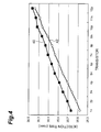
- Fig. 4 is a diagram showing emission timings of transistors in inverters.
- Fig. 5 is a diagram showing approximate curves of sequential line graphs shown in Fig. 4.
- Fig. 6 is a schematic plan view showing a plurality of detection positions on a surface of a micro channel plate.
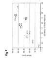
- Fig. 7 is a diagram showing the distribution of delays of detection times corresponding to a plurality of detection positions.
- Fig. 8 is a schematic view for explaining a method of measuring correction data.
- Fig. 9 is a diagram showing sampling points on an effective region.
- Fig. 10 is a diagram showing a 3D display of delays of detection times measured at the sampling points.
- Fig. 11 is a diagram showing a 3D display of delays after interpolation.
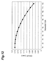
- Fig. 12 depicts the distribution of delays of detection times corresponding to the transistors in an inverter chain.
- Fig. 13 is a flowchart showing an example of the procedure of time-resolved measurement.
- Fig. 14 is a flowchart showing another example of the procedure of time-resolved measurement.
- Fig. 1 is a block diagram showing the configuration of a time-resolved measurement apparatus 100 according to the present embodiment.
- the apparatus 100 detects light 15 emitted from a sample 10 and measures the two-dimensional position and timing of the emission.
- the apparatus 100 has a semiconductor tester 12, position-sensitive photomultiplier tube (PS-PMT) 14, position-time measuring circuit 16, and data processor 18.
- PS-PMT position-sensitive photomultiplier tube
- a chip having a semiconductor integrated circuit (IC) thereon is prepared as an example of the sample 10.
- Fig. 2 is a schematic view showing the IC on the sample 10.
- This IC is an inverter chain 20 having twelve inverters 22 1 - 22 12 connected in series.
- a signal sequentially propagates from the first inverter 22 1 to the last inverter 22 12 along a direction shown as arrow 24.
- the signal propagation time between two adjacent inverters is theoretically designed as 70 ps.
- a MOS transistor forming an inverter sometimes emits light upon its switching. Therefore, by measuring the position and timing of the emission using the apparatus 100, it is feasible to determine when and which transistor is switched. This enables an analysis of operation of the inverter chain 20.
- the semiconductor tester 12 is an excitation device for exciting the sample 10 to cause emission of light.
- the tester 12 is electrically connected to the inverter chain 20 on the sample 10 and applies a drive voltage thereto.
- the tester 12 includes a signal generator 12a for generating a time reference pulse in synchronization with the application of the drive voltage. The time reference pulse is fed to the position-time measuring circuit 16.
- the position-sensitive photomultiplier tube 14 converts the light from the sample 10 into electrons and multiplies the electrons while maintaining the two-dimensional position thereof.
- the photomultiplier tube 14 has a photocathode, a micro channel plate (MCP), and a resistive anode.
- MCP micro channel plate
- the micro channel plate is located between the photocathode and the resistive anode.
- the front face of the micro channel plate is located opposite the photocathode, and the rear face opposite the resistive anode.
- Fig. 3 is a schematic plan view showing the micro channel plate. For simplicity of the drawing, Fig. 3 is illustrated without illustration of channels in the micro channel plate.
- the both end faces of the micro channel plate 30 are provided with an evaporated electroconductive material as electrodes 30a.
- the periphery of the micro channel plate 30 is covered with a metal flange 32 of ring shape.
- a lead terminal 34 is attached to one location on the flange 32.
- the lead terminal 34 is electrically conductive to the electrode 30a on the end face of the micro channel plate 30.
- the lead terminal 34 is connected to a position-time measuring circuit 16 by a lead wire.
- the micro channel plate 30 generates an electric pulse signal in synchronization with a timing at which light is detected. This pulse signal is fed to the circuit 16 through the lead terminal 34.
- the position-time measuring circuit 16 is electrically connected to both the tester 12 and the photomultiplier tube 14.
- the circuit 16 acts as a position calculator for calculating a detection position using a signal fed from the photomultiplier tube 14.
- the circuit 16 also acts as a time difference measuring device for measuring the time difference between the reference time pulse fed from the tester 12 and the detection timing pulse fed from the photomultiplier tube 14. This time difference indicates a detection time with respect to the reference time pulse.
- the detection position and the detection time determined by the circuit 16 are fed to the data processor 18.
- the data processor 18 receives the detection position and detection time from the position-time measuring circuit 16 and stores them in association with each other.
- the processor 18 is, for example, a personal computer.
- the processor 18 has a CPU, storage device, keyboard, mouse, and display.
- the storage device stores a data processing program to be executed by the CPU.
- the tester 12 activates the inverter chain 20 on the sample 10
- the plurality of inverters 22 operate in turn at intervals of about 70 ps.
- transistors in the inverters 22 emit light 15 with a certain probability.
- the photomultiplier tube 14 receives the light 15 on the photocathode.
- the photocathode converts the light 15 into a photoelectron by photoelectric effect.
- the photoelectron travels to the front face or input face of the micro channel plate by an electric field applied between the photocathode and the micro channel plate.
- the incidence position of the photoelectron on the micro channel plate corresponds to the incidence position of the light 15 on the photocathode.
- the micro channel plate generates at least one secondary electron at the incidence position of the photoelectron and multiplies the secondary electron while maintaining the two-dimensional position thereof. More specifically, the micro channel plate has a structure in which a number of very thin glass pipes are bundled. These glass pipes are channels. The inner wall of each channel is an electric resistor, and is an electron emitter also. The individual channels act as independent electron multipliers.
- a quantum e.g., a photoelectron in the present embodiment
- the secondary electrons travel along the channel while repeating collision with the inner wall, to be multiplied thereby.
- the two-dimensional position of secondary electrons is maintained by the channel.
- the secondary electrons reach the rear face of the micro channel plate, they are emitted from the rear face or output face of the micro channel plate by an electric field applied between the micro channel plate and the resistive anode, and collected to the resistive anode.
- the resistive anode is an electrical conductor plate provided with a uniform resistive layer on one surface. Electrodes for signal readout are provided at four positions in the periphery of the resistive anode. These electrodes are electrically connected to the position-time measuring circuit 16. When the secondary electrons enter the resistive anode, these reading electrodes emit charge pulses. The two-dimensional position of the secondary electrons incident on the resistive anode can be determined according to the amounts of charge of these charge pulses. In this manner, the resistive anode generates a signal according to the position at which the light 15 is detected and feeds the signal to the position-time measuring circuit 16.
- the circuit 16 receives the charge pulses from the electrodes at the four corners of the resistive anode in the photomultiplier tube 14, and calculates the two-dimensional position of the secondary electrons on the resistive anode by detection of the weighted center. This two-dimensional position corresponds to the two-dimensional position of the light emission on the sample 10. The position at which the light 15 is detected is determined in this manner. This detection position is sent to the data processor 18.
- the photomultiplier tube 14 generates a pulse in synchronization with a timing at which the light 15 is detected.
- This detection timing pulse is taken out of the micro channel plate 30. The generation of the detection timing pulse will be described below with reference to Fig. 3.
- a square region indicated by reference numeral 36 is a region in which the secondary electrons can be collected by the resistive anode in the rear face (output face) of the micro channel plate 30. This region will be referred to hereinafter as "effective region.”
- the inverters 22 1 - 22 12 emit light, photoelectrons are collected at positions 38 1 - 38 12 in the effective region 36 corresponding to the respective inverters 22 1 - 22 12 .
- the potential instantaneously increases on the output face of the micro channel plate 30.
- the circuit 16 receives the reference time pulse from the tester 12 immediately after the tester 12 activates the inverter chain 20 on the sample 10. Thereafter, the circuit 16 receives the detection timing pulse from the micro channel plate 30.
- the circuit 16 has a time-to-amplitude converter (TAC), and the reference time pulse and the detection timing pulse are fed to this time-to-amplitude converter.
- TAC time-to-amplitude converter
- the time-to-amplitude converter generates a voltage signal having a level corresponding to the time difference between the reference time pulse and the detection timing pulse. As described above, this time difference is equivalent to the detection time of the light 15 with respect to the time of excitation of the sample 10. This signal corresponding to the time difference will be referred to hereinafter as "detection time signal.”
- the detection time signal is fed from the circuit 16 to the data processor 18.
- the data processor 18 receives the detection position and the detection time signal from the circuit 16, corrects the detection time indicated by the detection time signal, and thereafter stores the detection position and the detection time in association with each other in the storage device. The correction for the detection time will be described later in detail.
- the sample 10 is repeatedly excited to accumulate the detection positions and the detection times in the data processor 18.
- the accumulated data can be utilized in various ways.
- the data processor 18 can be arranged to count the number of light emissions at each detection position over a certain period of time and generate a two-dimensional image in which luminances according to the counted numbers are assigned to pixels corresponding to the detection positions.
- the data processor 18 can be arranged to create a histogram of the detection times at a specific detection position, using the accumulated detection times. In this histogram, the horizontal axis represents the detection times and the vertical axis the number of light emissions.
- a peak in the histogram indicates a time at which light emissions at a specific detection position are detected at a high frequency. Therefore, the detection time corresponding to the peak can be regarded as a timing of the switching of the transistor corresponding to the detection position in the inverter 22.
- the inventors arranged the data processor 18 so as to store the detection position and the detection time without correction for the time difference. However, the inventors realized that this was unfavorable for the analysis of the sequential operation timings of multiple semiconductor devices such as the inverters 22 1 - 22 12 . This will be described with reference to Figs. 4 and 5.
- Fig. 4 shows light emission timings of the inverters 22 1 - 22 12 on the basis of data acquired in both the case with the correction for detection times and the case without the correction.
- numeral 40 denotes the emission timings in the case without the correction for detection times
- 42 the emission timings in the case with the correction for detection times.
- Fig. 5 shows approximate curves of these sequential line graphs 40 and 42.
- numeral 50 denotes an approximate curve in the case without the correction for detection times
- 52 an approximate curve in the case with the correction for detection times.
- the horizontal axis represents the transistors in the inverters 22 1 - 22 12
- the vertical axis the detection times the detection times.
- 1n, 3n, 5n, 7n, 9n, and 11n represent n-FETs in the respective inverters 22 1 , 22 3 , 22 5 , 22 7 , 22 9 , and 22 11 , and 2p, 4p, 6p, 8p, 10p, and 12p p-FETs in the respective inverters 22 2 , 22 4 , 22 6 , 22 8 , 22 10 , and 22 12 .
- the detection times on the vertical axis are determined as described above: a histogram is created for each inverter 22, using the detection positions and detection times accumulated in the data processor 18, and the detection time corresponding to a peak in the histogram is acquired by calculation.
- the inverter chain 20 is designed so that the transistors in the inverters 22 1 - 22 12 are sequentially subjected to switching at constant time intervals. Therefore, the slope of graph 50 must be constant as long as the measurement is accurate. In fact, however, the slope of graph 50 decreases as the transistor is located nearer the lead terminal 34. This means that the time interval of switching becomes gradually shorter in the result of the measurement.
- the inventors contemplates that the nonuniformity of switching timings in the result of the measurement is error due to variation in the propagation time of the detection timing pulse on the micro channel plate 30. This will be described below.
- the distance between the position 38 at which a detection timing pulse is generated and the lead terminal 34 differs depending on the position of the inverter 22. For this reason, detection timing pulses generated by photons emitted from different inverters 22 require different times for propagation from their generation position 38 to the lead terminal 34.
- the distance between detection position 38 1 corresponding to light emission of inverter 22 1 , and lead terminal 34 is 1 1
- the distance between detection position 38 6 corresponding to light emission of inverter 22 6 , and lead terminal 34 is 1 6 .
- the symbol "c" herein represents the speed of electromagnetic waves.
- the detection time delays from a time at which the light 15 is actually detected, i.e., a time at which the detection timing pulse is generated, by a time necessary for the detection timing pulse to propagate to the position-time measuring circuit 16. It is considered that since the delay differs depending on the detection positions 38 1 - 38 12 , the time intervals of the measured switching timings become nonuniform.
- the propagation time of each detection timing pulse is intricately affected by various factors, such as the shape of the flange 32, the structure and material of the micro channel plate 30, and so on.
- the number of the lead terminals does not have to be limited to 1, but a plurality of lead terminals may be installed for reduction in the absolute value of the delay (decrease in the distance from detection position 38 to lead terminal 34). In that case, the lead terminals preferably have the same length.
- An example in which the number of the lead terminals 34 is infinite is to use a cone electrode instead of the lead terminals, whereby the absolute value of the delay can be minimized.
- Fig. 6 is a schematic plan view showing a plurality of detection positions P1 - P14 on the micro channel plate 30, and Fig. 7 depicts the delays of the detection times corresponding to those positions.
- Fig. 6 is illustrated without illustration of the channels of the micro channel plate 30.
- the distribution of the delays shown in Fig. 7 reflects that the time to arrival at the lead terminal 34 becomes longer as the detection timing signal is generated at a position more distant from the lead terminal 34.
- the delays corresponding to the respective detection positions can be calculated using an electromagnetic field simulator or a high-frequency circuit simulator, or can be measured by a method as described later.
- the variation in the delays of the detection times according to the detection positions causes no problem in use in which light emitted from one location on the sample 10 is repeatedly measured.
- a problem will arise in the case of analyzing the sequential operation timings of multiple semiconductor devices located at different positions, as in the case of the inverter chain 20.
- the inverter 22 As shown in Fig. 3, as the inverter 22 becomes nearer the last one, it generates the detection timing pulse at the detection position 38 nearer the output terminal 34. Therefore, the inverter 22 nearer the last one has a shorter delay of the detection time. This nonuniformity of the delays produces the result of the measurement that the switching intervals, which should be constant, become gradually shorter.
- the inventors decided to arrange the data processor 18 so as to correct the variation in the delays according to the detection positions.
- This correction process is carried out using correction data that reflects the distribution of the delays on the micro channel plate 30.
- This correction data can be acquired by experiment, or can also be acquired by calculation using an electromagnetic field simulator or high-frequency circuit simulator.
- Fig. 8 is a schematic view showing the measurement method.
- a picosecond or subnanosecond pulse laser light source 40 is used instead of the tester 12 in the time-resolved measurement apparatus 100, and the distribution of the delays according to the detection positions of the laser light is determined.
- the laser light source 40 emits pulsed laser light and outputs a time reference signal in synchronization with the emission. This time reference signal is fed to the position-time measuring circuit 16.
- An optical fiber 42 is connected to the light source 40. The pulsed laser light emitted from the light source 40 propagates in the optical fiber 42 and emerges toward a lens 44.
- the laser light is focused by the lens 44 to enter a photocathode 50 of the photomultiplier tube 14.
- Photoelectrons generated by photoelectric effect in the photocathode 50 are multiplied by the micro channel plate to be emitted toward a resistive anode 52.
- the detection timing pulse generated at this time propagates on the rear face of the micro channel plate 30 to reach the lead terminal 34, and is then fed therefrom to the position-time measuring circuit 16.
- the resistive anode 52 feeds a signal corresponding to the detection position of the laser pulsed light, to the circuit 16.
- the circuit 16 calculates the detection position on the basis of the signal from the resistive anode and sends the calculated detection position to the data processor 18.
- the circuit 16 generates a signal corresponding to the time difference between the time reference pulse from light source 40 and the detection timing pulse, and sends the signal to the data processor 18. In this method, this time difference will be treated as the delay of the detection time according to the detection position.
- the data processor 18 stores the detection position and the delay sent from the circuit 16, in association with each other. The light is made incident to various positions on the photocathode 50 with two-dimensional movement of the output end 43 of the optical fiber using an X-Y stage (not shown), so as to accumulate the detection positions and the delays in the data processor 18.
- the data processor 18 assigns 512 ⁇ 512 pixels, i.e., approximately 260,000 pixels to the effective region 36 on the micro channel plate 30.
- a way of measuring the delay for each pixel by irradiating each pixel with the light is not practical because an extremely huge amount of time is necessary even if the measurement time per pixel is set to about 10 seconds. In view of this, it is effective to measure the delays for only several ten pixels and to calculate delays for the other pixels by interpolation.
- the effective region 36 is divided by a hypothetical mesh 53 and the delays are measured for only twenty five intersections 54 in the mesh 53. Namely, these intersections 54 are sampling points.
- Fig. 10 depicts a 3D display of the distribution of the delays measured at the sampling points 54. The delays corresponding to the positions between the sampling points 54 are calculated by two-dimensional spline interpolation.
- Fig. 11 depicts a 3D display of the distribution of the delays obtained by the interpolation. This interpolated delay distribution is used as correction data.
- Fig. 12 shows the delays corresponding to the transistors in the inverter chain 20 determined on the basis of the correction data shown in Fig. 11. As shown in Fig. 12, a transistor in an earlier position has a greater delay.
- the data processor 18 acquires a detection time from the circuit 16 by the time-resolved measurement of the sample 10 and thereafter subtracts the correction data from the detection time. Namely, the delay for each detection position is subtracted from the detection time for the same detection position. This subtraction removes the propagation time of the detection timing pulse from the detection time. Thus, it is possible to correct the error of the detection time due to the variation in the propagation time of the detection timing pulse.
- the data processor 18 stores the detection time thus corrected, in association with the detection position. Therefore, it is feasible to enhance the precision of the time-resolved measurement. Indeed, as indicated by graph 42 in Fig. 4 and graph 52 in Fig. 5, this correction arranges the detection times of light emissions from the transistors in the inverters 22 1 - 22 12 at approximately equal intervals, so as to achieve agreement with the design theory.
- the acquisition of the correction data may be done before the time-resolved measurement of sample 10 as shown in Fig. 13, or may be done after the time-resolved measurement as shown in Fig. 14.
- the first step is to acquire the correction data by the method described above with reference to Fig. 8 (step S130).
- This correction data is stored in the storage device in the data processor 18 (step S132).
- the apparatus 100 performs the time-resolved measurement of light emission from the inverter chain 20 by the method described above with reference to Fig. 1 (step S134).
- the data processor 18 subtracts the correction data from the acquired measurement data to correct the time error in the measurement data (step S136).
- the measurement data after the correction is stored in the storage device and is also displayed in the form of a sequential line graph as shown in Fig. 4, on the display of the data processor 18 (step S138).
- the first step is to perform the time-resolved measurement of the inverter chain 20 by the apparatus 100 (step S140), and the next step is to store the obtained measurement data in the storage device in the data processor 18 (step S142). Thereafter, the correction data for time error is acquired by the method shown in Fig. 8 (step S144).
- the data processor 18 reads the measurement data from the storage device and subtracts the correction data therefrom to correct the time error (step S146).
- the corrected measurement data is stored in the storage device and is also displayed on the display (step S148).
- the correction data is acquired by the measurement shown in Fig. 8.
- the correction data may be acquired by calculation.
- the foregoing delay distribution can be calculated using an electromagnetic field simulator or high-frequency circuit simulator.
- a "photomultiplier tube (PMT)” is one of the embodiments of an “electron multiplier tube (EMT).”
- the embodiments mentioned above use the position-sensitive photomultiplier tube (PS-PMT).
- PS-PMT position-sensitive photomultiplier tube
- the micro channel plates are not sensitive only to electron beams but are also sensitive directly to other quantum beams, such as ultraviolet rays (UV and VUV), X-rays, ⁇ -rays, charged particles, and neutrons. Which of a PS-PMT and a PS-EMT is to be used is properly determined depending on the type of a quantum beam emitted from an object to be detected.
- the above embodiment uses the resistive anode 28 as a position-sensitive anode.
- any other position-sensitive anodes e.g., multi-anodes, a CR chain type anode, a cross-wire anode, and a semiconductor position-sensitive detector (PSD).
- PSD semiconductor position-sensitive detector
- the position of secondary electrons may also be measured by using a fluorescent screen, as an anode, for converting the secondary electrons into an optical image and taking the optical image by use of an image sensor.
- the fluorescent screen may be fiber-coupled with the image sensor through a fiber plate.
- time-resolved detection takes up the analysis of the operation of the semiconductor integrated circuit.
- time-resolved detection can be applied to a wide variety of applications, and the present invention can be applied to various measurement techniques including Time of Flight (TOF) application, e.g., secondary ion mass spectroscopy (SIMS), ion scattering spectroscopy (ISS), an atom probe, and so on.
- TOF Time of Flight
- SIMS secondary ion mass spectroscopy
- ISS ion scattering spectroscopy
- atom probe e.g., an atom probe, and so on.
- the time-resolved measurement apparatus of the present invention corrects the nonuniformity of the detection time delay according to the detection position, whereby it is able to cancel the error of the detection time and to enhance the precision of the time-resolved measurement.
Landscapes
- Health & Medical Sciences (AREA)
- Nuclear Medicine, Radiotherapy & Molecular Imaging (AREA)
- Physics & Mathematics (AREA)
- Life Sciences & Earth Sciences (AREA)
- Chemical & Material Sciences (AREA)
- Analytical Chemistry (AREA)
- Biochemistry (AREA)
- General Health & Medical Sciences (AREA)
- General Physics & Mathematics (AREA)
- Immunology (AREA)
- Pathology (AREA)
- Investigating, Analyzing Materials By Fluorescence Or Luminescence (AREA)
- Testing Or Measuring Of Semiconductors Or The Like (AREA)
- Electron Tubes For Measurement (AREA)
- Analysing Materials By The Use Of Radiation (AREA)
- Other Investigation Or Analysis Of Materials By Electrical Means (AREA)
- Measurement Of Radiation (AREA)
- Measurement Of Unknown Time Intervals (AREA)
Applications Claiming Priority (2)
| Application Number | Priority Date | Filing Date | Title |
|---|---|---|---|
| JP2003179775A JP4268461B2 (ja) | 2003-06-24 | 2003-06-24 | 時間分解測定装置 |
| PCT/JP2004/009268 WO2004113888A1 (fr) | 2003-06-24 | 2004-06-24 | Appareil de mesure par resolution du temps |
Publications (1)
| Publication Number | Publication Date |
|---|---|
| EP1640711A1 true EP1640711A1 (fr) | 2006-03-29 |
Family
ID=33535088
Family Applications (1)
| Application Number | Title | Priority Date | Filing Date |
|---|---|---|---|
| EP04746737A Withdrawn EP1640711A1 (fr) | 2003-06-24 | 2004-06-24 | Appareil de mesure par resolution du temps |
Country Status (7)
| Country | Link |
|---|---|
| US (1) | US7425694B2 (fr) |
| EP (1) | EP1640711A1 (fr) |
| JP (1) | JP4268461B2 (fr) |
| KR (1) | KR101058672B1 (fr) |
| CN (1) | CN100473974C (fr) |
| TW (1) | TWI331214B (fr) |
| WO (1) | WO2004113888A1 (fr) |
Families Citing this family (13)
| Publication number | Priority date | Publication date | Assignee | Title |
|---|---|---|---|---|
| JP4268463B2 (ja) * | 2003-06-25 | 2009-05-27 | 浜松ホトニクス株式会社 | 時間分解測定装置および位置検出型電子増倍管 |
| CN101689355A (zh) * | 2007-06-15 | 2010-03-31 | 路迪亚公司 | 大平板显示器中的交互性 |
| JP5474312B2 (ja) * | 2007-06-20 | 2014-04-16 | 株式会社日立ハイテクノロジーズ | 荷電粒子ビーム装置及びその制御方法 |
| JP5181150B2 (ja) * | 2008-04-09 | 2013-04-10 | 独立行政法人科学技術振興機構 | 表面分析方法 |
| EP2199830B1 (fr) * | 2008-12-19 | 2014-07-02 | Leibniz-Institut für Neurobiologie | Appareil de mesure de résolution de position et procédé d'acquisition de coordonnées d'espace d'un faisceau quantique incident |
| JP4620786B2 (ja) * | 2009-02-17 | 2011-01-26 | 三井造船株式会社 | 蛍光検出方法、蛍光検出装置及びプログラム |
| JP5582493B2 (ja) * | 2009-12-17 | 2014-09-03 | 独立行政法人理化学研究所 | マイクロチャネルプレート組立体及びマイクロチャネルプレート検出器 |
| US8389929B2 (en) * | 2010-03-02 | 2013-03-05 | Thermo Finnigan Llc | Quadrupole mass spectrometer with enhanced sensitivity and mass resolving power |
| US9128076B2 (en) * | 2010-04-30 | 2015-09-08 | Exxonmobil Upstream Research Company | Measurement of isotope ratios in complex matrices |
| JP2015233169A (ja) * | 2012-09-25 | 2015-12-24 | 富士フイルム株式会社 | 放射線画撮影装置、放射線動画撮影システム、放射線画撮影装置の制御方法、及び放射線画撮影制御プログラム |
| CA2957543A1 (fr) | 2014-08-08 | 2016-02-11 | Quantum-Si Incorporated | Systeme optique et puce d'analyse pour sonder, detecter, et analyser des molecules |
| JP6486090B2 (ja) * | 2014-12-09 | 2019-03-20 | キヤノン株式会社 | 放射線撮像システム及びその制御方法 |
| JP7217158B2 (ja) * | 2019-01-24 | 2023-02-02 | 株式会社ダイセル | 航空機用部材、及びその製造方法 |
Family Cites Families (8)
| Publication number | Priority date | Publication date | Assignee | Title |
|---|---|---|---|---|
| JPS60220542A (ja) | 1984-04-17 | 1985-11-05 | Hamamatsu Photonics Kk | 入射位置情報を取出し可能な光電子増倍装置 |
| JPS61266942A (ja) * | 1985-05-21 | 1986-11-26 | Hamamatsu Photonics Kk | 2次元微弱発光測定装置 |
| US5386827A (en) * | 1993-03-30 | 1995-02-07 | Nim Incorporated | Quantitative and qualitative in vivo tissue examination using time resolved spectroscopy |
| JP3071809B2 (ja) * | 1990-09-07 | 2000-07-31 | 浜松ホトニクス株式会社 | ストリーク管 |
| JP2875370B2 (ja) * | 1990-09-14 | 1999-03-31 | 浜松ホトニクス株式会社 | 荷電粒子測定装置および光強度波形測定装置 |
| JPH07211280A (ja) | 1994-01-19 | 1995-08-11 | Hamamatsu Photonics Kk | 位置検出型光電子増倍管 |
| US5940545A (en) | 1996-07-18 | 1999-08-17 | International Business Machines Corporation | Noninvasive optical method for measuring internal switching and other dynamic parameters of CMOS circuits |
| JP4459390B2 (ja) * | 2000-06-08 | 2010-04-28 | 浜松ホトニクス株式会社 | 蛍光測定方法、蛍光測定装置及びそれを用いた試料評価装置 |
-
2003
- 2003-06-24 JP JP2003179775A patent/JP4268461B2/ja not_active Expired - Fee Related
-
2004
- 2004-06-21 TW TW093117920A patent/TWI331214B/zh not_active IP Right Cessation
- 2004-06-24 KR KR1020057020479A patent/KR101058672B1/ko not_active Expired - Fee Related
- 2004-06-24 CN CNB2004800176060A patent/CN100473974C/zh not_active Expired - Fee Related
- 2004-06-24 WO PCT/JP2004/009268 patent/WO2004113888A1/fr not_active Ceased
- 2004-06-24 EP EP04746737A patent/EP1640711A1/fr not_active Withdrawn
- 2004-06-24 US US10/561,938 patent/US7425694B2/en not_active Expired - Fee Related
Non-Patent Citations (1)
| Title |
|---|
| See references of WO2004113888A1 * |
Also Published As
| Publication number | Publication date |
|---|---|
| TW200508595A (en) | 2005-03-01 |
| US20070267565A1 (en) | 2007-11-22 |
| CN100473974C (zh) | 2009-04-01 |
| JP2005019537A (ja) | 2005-01-20 |
| WO2004113888A1 (fr) | 2004-12-29 |
| KR101058672B1 (ko) | 2011-08-22 |
| KR20060024368A (ko) | 2006-03-16 |
| CN1809741A (zh) | 2006-07-26 |
| TWI331214B (en) | 2010-10-01 |
| JP4268461B2 (ja) | 2009-05-27 |
| US7425694B2 (en) | 2008-09-16 |
Similar Documents
| Publication | Publication Date | Title |
|---|---|---|
| EP2199830B1 (fr) | Appareil de mesure de résolution de position et procédé d'acquisition de coordonnées d'espace d'un faisceau quantique incident | |
| JP4268463B2 (ja) | 時間分解測定装置および位置検出型電子増倍管 | |
| JP6152403B2 (ja) | 感度および質量分解能が増強された多重極型質量分析方法 | |
| US7425694B2 (en) | Time-resolved measurement apparatus | |
| AU2014354949B2 (en) | Detectors and methods of using them | |
| WO2010070111A1 (fr) | Appareil de mesure résolue dans le temps et détecteur sensible au temps avec amélioration de la mesure du temps | |
| US8803083B2 (en) | Time of flight mass spectrometer | |
| JP2006505900A (ja) | 荷電粒子スペクトロメータおよびその検出器 | |
| JP2024008919A (ja) | 質量分析法におけるイオンピーク面積の処理 | |
| US5087814A (en) | Method and apparatus for counting charged particles | |
| Smirnov et al. | Precision measurements of time characteristics of ETL9351 photomultipliers | |
| Bieniosek et al. | Beam imaging diagnostics for heavy ion beam fusion experiments | |
| Renaud et al. | Design of a fast multi-hit position sensitive detector based on a CCD camera | |
| Ivanisenko et al. | PHOTO INJECTOR CATHODE LASER BEAM INTENSITY AND POINTING STABILITY DIAGNOSTICS. | |
| Ivanisenko | Photoinjector laser intensity and pointing position monitoring system | |
| Oba et al. | Microchannel plate as a detector of minimum ionizing particle | |
| Ivanisenko et al. | EUROFEL-Report-2007-DS1-039 |
Legal Events
| Date | Code | Title | Description |
|---|---|---|---|
| PUAI | Public reference made under article 153(3) epc to a published international application that has entered the european phase |
Free format text: ORIGINAL CODE: 0009012 |
|
| 17P | Request for examination filed |
Effective date: 20060105 |
|
| AK | Designated contracting states |
Kind code of ref document: A1 Designated state(s): DE FR GB |
|
| DAX | Request for extension of the european patent (deleted) | ||
| RBV | Designated contracting states (corrected) |
Designated state(s): DE FR GB |
|
| STAA | Information on the status of an ep patent application or granted ep patent |
Free format text: STATUS: THE APPLICATION HAS BEEN WITHDRAWN |
|
| 18W | Application withdrawn |
Effective date: 20140226 |