EP1640949A2 - Méthode de design et écran d'affichage et dispositif électronique utilisant le même écran - Google Patents
Méthode de design et écran d'affichage et dispositif électronique utilisant le même écran Download PDFInfo
- Publication number
- EP1640949A2 EP1640949A2 EP05108741A EP05108741A EP1640949A2 EP 1640949 A2 EP1640949 A2 EP 1640949A2 EP 05108741 A EP05108741 A EP 05108741A EP 05108741 A EP05108741 A EP 05108741A EP 1640949 A2 EP1640949 A2 EP 1640949A2
- Authority
- EP
- European Patent Office
- Prior art keywords
- light component
- light
- emission
- driving unit
- components
- Prior art date
- Legal status (The legal status is an assumption and is not a legal conclusion. Google has not performed a legal analysis and makes no representation as to the accuracy of the status listed.)
- Withdrawn
Links
Images





Classifications
-
- G—PHYSICS
- G09—EDUCATION; CRYPTOGRAPHY; DISPLAY; ADVERTISING; SEALS
- G09G—ARRANGEMENTS OR CIRCUITS FOR CONTROL OF INDICATING DEVICES USING STATIC MEANS TO PRESENT VARIABLE INFORMATION
- G09G3/00—Control arrangements or circuits, of interest only in connection with visual indicators other than cathode-ray tubes
- G09G3/20—Control arrangements or circuits, of interest only in connection with visual indicators other than cathode-ray tubes for presentation of an assembly of a number of characters, e.g. a page, by composing the assembly by combination of individual elements arranged in a matrix no fixed position being assigned to or needed to be assigned to the individual characters or partial characters
- G09G3/22—Control arrangements or circuits, of interest only in connection with visual indicators other than cathode-ray tubes for presentation of an assembly of a number of characters, e.g. a page, by composing the assembly by combination of individual elements arranged in a matrix no fixed position being assigned to or needed to be assigned to the individual characters or partial characters using controlled light sources
- G09G3/30—Control arrangements or circuits, of interest only in connection with visual indicators other than cathode-ray tubes for presentation of an assembly of a number of characters, e.g. a page, by composing the assembly by combination of individual elements arranged in a matrix no fixed position being assigned to or needed to be assigned to the individual characters or partial characters using controlled light sources using electroluminescent panels
- G09G3/32—Control arrangements or circuits, of interest only in connection with visual indicators other than cathode-ray tubes for presentation of an assembly of a number of characters, e.g. a page, by composing the assembly by combination of individual elements arranged in a matrix no fixed position being assigned to or needed to be assigned to the individual characters or partial characters using controlled light sources using electroluminescent panels semiconductive, e.g. using light-emitting diodes [LED]
- G09G3/3208—Control arrangements or circuits, of interest only in connection with visual indicators other than cathode-ray tubes for presentation of an assembly of a number of characters, e.g. a page, by composing the assembly by combination of individual elements arranged in a matrix no fixed position being assigned to or needed to be assigned to the individual characters or partial characters using controlled light sources using electroluminescent panels semiconductive, e.g. using light-emitting diodes [LED] organic, e.g. using organic light-emitting diodes [OLED]
- G09G3/3225—Control arrangements or circuits, of interest only in connection with visual indicators other than cathode-ray tubes for presentation of an assembly of a number of characters, e.g. a page, by composing the assembly by combination of individual elements arranged in a matrix no fixed position being assigned to or needed to be assigned to the individual characters or partial characters using controlled light sources using electroluminescent panels semiconductive, e.g. using light-emitting diodes [LED] organic, e.g. using organic light-emitting diodes [OLED] using an active matrix
- G09G3/3233—Control arrangements or circuits, of interest only in connection with visual indicators other than cathode-ray tubes for presentation of an assembly of a number of characters, e.g. a page, by composing the assembly by combination of individual elements arranged in a matrix no fixed position being assigned to or needed to be assigned to the individual characters or partial characters using controlled light sources using electroluminescent panels semiconductive, e.g. using light-emitting diodes [LED] organic, e.g. using organic light-emitting diodes [OLED] using an active matrix with pixel circuitry controlling the current through the light-emitting element
-
- G—PHYSICS
- G09—EDUCATION; CRYPTOGRAPHY; DISPLAY; ADVERTISING; SEALS
- G09G—ARRANGEMENTS OR CIRCUITS FOR CONTROL OF INDICATING DEVICES USING STATIC MEANS TO PRESENT VARIABLE INFORMATION
- G09G2300/00—Aspects of the constitution of display devices
- G09G2300/04—Structural and physical details of display devices
- G09G2300/0439—Pixel structures
- G09G2300/0452—Details of colour pixel setup, e.g. pixel composed of a red, a blue and two green components
-
- G—PHYSICS
- G09—EDUCATION; CRYPTOGRAPHY; DISPLAY; ADVERTISING; SEALS
- G09G—ARRANGEMENTS OR CIRCUITS FOR CONTROL OF INDICATING DEVICES USING STATIC MEANS TO PRESENT VARIABLE INFORMATION
- G09G2300/00—Aspects of the constitution of display devices
- G09G2300/08—Active matrix structure, i.e. with use of active elements, inclusive of non-linear two terminal elements, in the pixels together with light emitting or modulating elements
- G09G2300/0809—Several active elements per pixel in active matrix panels
- G09G2300/0819—Several active elements per pixel in active matrix panels used for counteracting undesired variations, e.g. feedback or autozeroing
-
- G—PHYSICS
- G09—EDUCATION; CRYPTOGRAPHY; DISPLAY; ADVERTISING; SEALS
- G09G—ARRANGEMENTS OR CIRCUITS FOR CONTROL OF INDICATING DEVICES USING STATIC MEANS TO PRESENT VARIABLE INFORMATION
- G09G2300/00—Aspects of the constitution of display devices
- G09G2300/08—Active matrix structure, i.e. with use of active elements, inclusive of non-linear two terminal elements, in the pixels together with light emitting or modulating elements
- G09G2300/0809—Several active elements per pixel in active matrix panels
- G09G2300/0842—Several active elements per pixel in active matrix panels forming a memory circuit, e.g. a dynamic memory with one capacitor
-
- G—PHYSICS
- G09—EDUCATION; CRYPTOGRAPHY; DISPLAY; ADVERTISING; SEALS
- G09G—ARRANGEMENTS OR CIRCUITS FOR CONTROL OF INDICATING DEVICES USING STATIC MEANS TO PRESENT VARIABLE INFORMATION
- G09G2320/00—Control of display operating conditions
- G09G2320/02—Improving the quality of display appearance
- G09G2320/0233—Improving the luminance or brightness uniformity across the screen
-
- G—PHYSICS
- G09—EDUCATION; CRYPTOGRAPHY; DISPLAY; ADVERTISING; SEALS
- G09G—ARRANGEMENTS OR CIRCUITS FOR CONTROL OF INDICATING DEVICES USING STATIC MEANS TO PRESENT VARIABLE INFORMATION
- G09G2320/00—Control of display operating conditions
- G09G2320/04—Maintaining the quality of display appearance
- G09G2320/043—Preventing or counteracting the effects of ageing
-
- G—PHYSICS
- G09—EDUCATION; CRYPTOGRAPHY; DISPLAY; ADVERTISING; SEALS
- G09G—ARRANGEMENTS OR CIRCUITS FOR CONTROL OF INDICATING DEVICES USING STATIC MEANS TO PRESENT VARIABLE INFORMATION
- G09G2320/00—Control of display operating conditions
- G09G2320/06—Adjustment of display parameters
- G09G2320/0666—Adjustment of display parameters for control of colour parameters, e.g. colour temperature
-
- G—PHYSICS
- G09—EDUCATION; CRYPTOGRAPHY; DISPLAY; ADVERTISING; SEALS
- G09G—ARRANGEMENTS OR CIRCUITS FOR CONTROL OF INDICATING DEVICES USING STATIC MEANS TO PRESENT VARIABLE INFORMATION
- G09G2360/00—Aspects of the architecture of display systems
- G09G2360/14—Detecting light within display terminals, e.g. using a single or a plurality of photosensors
- G09G2360/145—Detecting light within display terminals, e.g. using a single or a plurality of photosensors the light originating from the display screen
- G09G2360/147—Detecting light within display terminals, e.g. using a single or a plurality of photosensors the light originating from the display screen the originated light output being determined for each pixel
- G09G2360/148—Detecting light within display terminals, e.g. using a single or a plurality of photosensors the light originating from the display screen the originated light output being determined for each pixel the light being detected by light detection means within each pixel
-
- G—PHYSICS
- G09—EDUCATION; CRYPTOGRAPHY; DISPLAY; ADVERTISING; SEALS
- G09G—ARRANGEMENTS OR CIRCUITS FOR CONTROL OF INDICATING DEVICES USING STATIC MEANS TO PRESENT VARIABLE INFORMATION
- G09G3/00—Control arrangements or circuits, of interest only in connection with visual indicators other than cathode-ray tubes
- G09G3/20—Control arrangements or circuits, of interest only in connection with visual indicators other than cathode-ray tubes for presentation of an assembly of a number of characters, e.g. a page, by composing the assembly by combination of individual elements arranged in a matrix no fixed position being assigned to or needed to be assigned to the individual characters or partial characters
- G09G3/22—Control arrangements or circuits, of interest only in connection with visual indicators other than cathode-ray tubes for presentation of an assembly of a number of characters, e.g. a page, by composing the assembly by combination of individual elements arranged in a matrix no fixed position being assigned to or needed to be assigned to the individual characters or partial characters using controlled light sources
-
- G—PHYSICS
- G09—EDUCATION; CRYPTOGRAPHY; DISPLAY; ADVERTISING; SEALS
- G09G—ARRANGEMENTS OR CIRCUITS FOR CONTROL OF INDICATING DEVICES USING STATIC MEANS TO PRESENT VARIABLE INFORMATION
- G09G5/00—Control arrangements or circuits for visual indicators common to cathode-ray tube indicators and other visual indicators
- G09G5/02—Control arrangements or circuits for visual indicators common to cathode-ray tube indicators and other visual indicators characterised by the way in which colour is displayed
Definitions
- the disclosure relates to a design approach, and more particularly to a design approach for improving brightness emitted from light component sources on a panel. More specifically, the present invention related to a method for designing a driving unit of a luminiferous unit such as a panel for improving the brightness emitted from light component sources thereof.
- Fig. 1 is a schematic diagram of a panel.
- Panel 1 comprises pixel units P11 ⁇ Pmn arranged in an array and a white light source, such as white EL(Electroluminescent) device.
- a white light source such as white EL(Electroluminescent) device.
- Each pixel unit comprises three white light sub-pixels, and each sub-pixel comprises three primary color components that make up a resultant white light for each sub-pixel.
- pixel unit P 11 comprises three white light sub-pixels P 11R , P 11G , P 11B , each make up of a combination of red, green, and blue colors.
- the resultant white light emission from each sub-pixel is filtered by a color filter, to render a color light to a viewer.
- Pixel unit P 11 would be provided with a red color filter over the sub-pixel P 11R , a green color filter over the sub-pixel P 11G , and a blue color filter over the sub-pixel P 11B .
- the pixel unit P 11 can be controlled to produce a color image of a desired overall color, by controlling the relative intensity of the respective white sub-pixels, to produce color lights of the desired relative intensity as viewed through the corresponding color filters.
- the intensity of the white EL devices often decreases significantly with operation due to the substantial property of three primary color components.
- the conventional method for compensating this shift in intensity utilizes photo sensors to detect the brightness of sub-pixels.
- the conventional method does not appropriately to compensate the brightness of the red light and the green light as a photo TFT is utilized to detect the brightness.
- the present invention is directed to a novel design approach for a panel comprising a luminiferous unit and driving unit.
- the luminiferous unit comprises first and second color components respectively constituting a first and a second light component sources.
- First and second light components are respectively emitted from the first and the second light component sources.
- the color of the first light component differs from that of the second light component.
- a specific relationship of a characteristic between the first and the second color components is defined.
- the driving unit is designed according to the specific relationship.
- the control method determines a change in emission of a desired light component out of several light components within a single color sub-pixel in an EL device. First, a relationship between changes in emissions of the several light components of the sub-pixel over a certain time period is predetermined. One of the several light components is designated a reference light component. Next, a change in emission of the reference light component in the sub-pixel is detected. Finally, a corresponding change in emission of the desired light component is determined and based on the predetermined relationship in reference to the detected emission of the reference light component.
- An exemplary embodiment of a panel comprises a luminiferous unit and a driving unit.
- the luminiferous unit comprises a first color component constituting a first light component source and a second color component constituting a second light component source.
- a first and a second light components are emitted from the first and the second light component sources.
- the color of the first light component differs from that of the second light component.
- a specific relationship is gained according to a characteristic between the first and the second color components.
- the driving unit is designed according to the specific relationship for driving the luminiferous unit
- An exemplary embodiment of an electronic device comprises a panel, a data driver, and a scan driver.
- the panel comprises a luminiferous unit and a driving unit.
- the luminiferous unit comprises a first color component constituting a first light component source and a second color component constituting a second light component source.
- a first light component is emitted from the first light component source.
- a second light component is emitted from the second light component source.
- the color of the first light component differs from that of the second light component.
- a specific relationship is gained according to a characteristic between the first and the second color components.
- the driving unit is designed according to the specific relationship for driving the luminiferous unit.
- the data driver supplies data signals to the driving unit.
- the scan driver supplies data signals to the driving unit.
- Fig. 2 is a schematic diagram of an embodiment of an electronic device.
- An electronic device 2 such as a PDA, a display monitor, a notebook computer, a tablet computer, or a cellular phone, comprises an adapter 3 and a panel 26. Panel 26 is powered by power output from adapter 3.
- Electronic device 2 further comprises a scan driver 22 and a data driver 24.
- Scan driver 22 supplies scan signals G 1 ⁇ G n to gate electrodes.
- Data driver 24 supplies data signals S 1R ⁇ S mB to source electrodes.
- Panel 26 comprises sub-pixels P 11R ⁇ P mnB , each comprising a driving unit and a luminiferous unit, such as an electroluminescent light device (ELD) comprising organic light emitting diode (OLED).
- ELD electroluminescent light device
- OLED organic light emitting diode
- data signal S 1R and scan signal G 1 control the sub-pixel P 11R which comprises a driving unit D 11R and a luminiferous unit EL 11R ⁇
- Driving unit D 11R drives luminiferous unit EL 11R according to scan signal G 1 output from data driver 24 and data signal S 1R output from scan driver 22.
- driving unit D 11R can detect and compensate for the brightness emitted from luminiferous unit EL 11R .
- a white light emitted from luminiferous units on panel 26 is a composite of several light components.
- Each luminiferous unit in the panel 26 may have several different types of color components to emit different light components.
- the white light emitted from panel 26 comprises a green light component, a blue light component, and a red light component.
- the white light can be constituted by two light components, such as a blue light component and a red light component.
- the composite light component emitted by the luminiferous units may be other than white.
- a specific relationship between different color components is predetermined according to the aging characteristics thereof.
- a detector (not shown) detects brightness emitted from panel 26 at a first and a second time. Then, a specific relationship is determined according to a ratio among the emission variable quantities of the red, the green, and the blue light components between the first and the second time. In other words, the specific relationship is the emission variable quantities of the red, the green, and the blue light components in a specific time range.
- a producer of electronic device 2 can design driving units D 11 ⁇ D mn according to the specific relationship after the specific relationship has been determined.
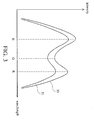
- Fig. 3 shows a characteristic curve of the specific relationship.
- Curve 30 indicates a relationship of the intensity and wavelength of various color components of the white light detected by a detector at time to.
- Curve 31 indicates a relationship of the intensity and wavelength of the white light detected by the detector at time t 1 .
- intensity has a direct ratio to brightness.
- Label B indicates the wavelength of a blue light component.
- Label G indicates the wavelength of a green light component.
- Label R indicates the wavelength of a red light component.
- C1 and C2 are transformation parameters.
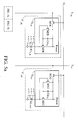
- Fig. 4 is a schematic diagram of an embodiment of a sup-pixel.
- a panel comprises a plurality of sub-pixels.
- Fig. 4 only shows a sub-pixel.
- a source/drain and a drain/source respectively indicate two terminal of the transistor in the following.
- Driving unit D 11R comprises transistors M1R ⁇ M3R and capacitor Cst R .
- the gate, or the control terminal, of the transistor M1R receives a scan signal G 1 in gate electrode and the drain/source thereof receives a data signal S 1R in source electrode.
- the source/drain of the transistor M2R is coupled to a high voltage source Power and the drain/source thereof is coupled to luminiferous unit EL 11R .
- the gate of the transistor M3R is coupled to luminiferous unit EL 11R , the drain/source thereof is coupled to the source/drain of the transistor M1R and the high voltage source Power, and the source/drain thereof is coupled to the gate of the transistor M2R.
- Capacitor Cst R is coupled between the source/drain and the gate of the transistor M2R.
- Luminiferous unit EL 11R emits a white light as transistor M2R is turned on by capacitor Cst R .
- the white light is constituted by a red light component L 1 , a green light component L 2 , and a blue light component L 3 .
- Transistor M3R can be formed by a low temperature poly silicon (LTPS) or amorphous silicon technology. Transistor M3R can be a photo diode or a photo transistor to detect and compensate for the brightness emitted from luminiferous unit EL 11R . In this embodiment, transistor M3R is a photo transistor for detecting the blue light component within the white light emitted from luminiferous unit EL 11R , as a reference color component.
- LTPS low temperature poly silicon
- Transistor M3R can be a photo diode or a photo transistor to detect and compensate for the brightness emitted from luminiferous unit EL 11R .
- transistor M3R is a photo transistor for detecting the blue light component within the white light emitted from luminiferous unit EL 11R , as a reference color component.
- the size of transistor M3R is defined for compensating the red color component based on the reference blue color component and the specific relationship.
- the size is a ratio between a length and a width of a channel of transistor M3R.
- capacitance of capacitor Cst R can be also defined by the specific relationship.
- the driving unit D 11R can be designed to change a current passing through luminiferous unit EL 11R or luminiferous time of luminiferous unit EL 11R to compensate for the brightness emitted from luminiferous unit EL 11R .
- transistor M3R detects and compensates for the brightness emitted from luminiferous unit EL 11R .
- Transistor M3R controls a discharge time of capacitor Cst R according to the brightness emitted from luminiferous unit EL 11R .
- the discharge time is slower, the enabling status time of transistor M2R is longer.
- the above compensation circuit could be provided in all the sub-pixels in a similar fashion, for compensating a desired light component in each sub-pixel, based on a reference light component detected in the sub-pixel, and the predetermined relationship.
- Figs. 5a and 5b are schematic diagrams of three sub-pixels.
- Sub-pixels P 11R , P 11G , P 11B respectively display a red light component, a green light component, and a blue light component.
- Driving units D 11R , D 11G , D 11B respectively drive luminiferous units EL 11R , EL 11G , EL 11B to emit a white light according to data signals S 11R , S 11G , S 11B output from source electrodes.
- luminiferous units EL 11R , EL 11G , EL 11B respectively emit a white light
- color filters can be utilized to render a required light component from a white light such that sub-pixels P 11R , P 11G , P 11B display the required light component.
- sub-pixel P 11R desires to display a red light
- a red color filter is utilized for filtering the red light from a white light emitted from luminiferous unit EL 11R ⁇
- transistors M3R, M3G, M3B are respectively utilized to change the discharge time of capacitor Cst R , Cst G , Cst B for compensating brightness of the respective red, green, and blue light components in the respective sub-pixels.
- sub-pixel P 11R when the channel size of transistor M3R is greater, the discharge time of capacitor Cst R is shorter, such that the luminiferous time of luminiferous unit EL11R is shorter.
- the structures of the compensating driving components i.e., M3R, M3G and M3B in the illustrated embodiment
- the intensity decay rate among the red, green, and blue light components constituting white light within a sub-pixel is 2:(1.5):1
- the relative channel size ratio among transistors M3R, M3G, M3B is 1:(1.5):2.
- the brightness of white lights emitted from luminiferous units EL 11R , EL 11G , EL 11B are defined by data signals S 11R , S 11G , S 11B from source electrodes.
- the brightness of white lights emitted from luminiferous units EL 11R , EL 11G , EL 11B may be 200nits for example.
- the emission of a white light emitted from luminiferous unit EL 11R decays to 100nits, the emission of red light component L 1 , the emission of green light component L 2 , and the emission of blue light component L 3 forming the brightness of the white light are decayed.
- transistor M3R When the decay quantity of the blue light component of the white lights is detected by transistor M3R, transistor M3R will decrease the discharge time of capacitor Cst R to increase the turn time of transistor M2R such that lumiferous times of the white lights are increased to compensate for the emission of the white light emitted from luminiferous unit EL 11R .
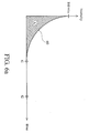
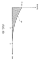
- Figs. 6a and 6b show characteristic curves of a luminiferous unit, comprising time and brightness.
- Curve 60 indicates a normal brightness emitted from the luminiferous unit.
- Curve 61 indicates a compensated brightness emitted from the luminiferous unit. Compare Fig. 6a with Fig. 6b, the maximum brightness in Fig. 6a exceeds that in Fig. 6b but the luminiferous time in Fig. 6a is less than that in Fig. 6b. Therefore, region A is equal to region B such that the efficiency of the normal brightness equals the compensated brightness.
- FIG. 7 is a flowchart of an embodiment of a design approach.
- the design approach is applied to a panel comprising a luminiferous unit and a driving unit.
- the luminiferous unit comprises first and second color components respectively constituting a first and a second light component sources.
- a first and a second light components are respectively emitted from the first and the second light component sources.
- the color of the first light component differs from that of the second light component.
- a specific relationship is predetermined according to a characteristic between the first and the second color components in step 710. Since each color component has an aging characteristic, the brightness of a first and a second light components will decay within a specific time range.
- the first and the second light component sources are constituted by different color components, the brightness variable quantity of the first light component differs that of the second light component within the specific time range.
- the specific time range is between a first time and a second time more than the first time.
- the specific relationship is a ratio between the brightness variable quantities of the first and the second light components.
- each color components has the aging characteristic and the second time exceeds the first time, the brightness of the first and the second light components detected in the second time are darker than that detected in the first time.
- the driving unit is designed according to the specific relationship in step 720. Since the aging characteristics of color components will effect the brightness of the first and the second light components, when the driving unit is designed according to the specific relationship, the brightness of the first and the second light components can be compensated.
- size of transistors M1R ⁇ M3R, M1G ⁇ M3G, M1B ⁇ M3B, or capacitance of capacitor Cst R , Cst G , Cst B can be changed for compensating aging characteristics of the first and the second color components.
- the channel size of transistor M3R, M3B, M3G are changed. If the aging speed of color component is faster, the channel size of the transistor is smaller.
- the driving unit When the driving unit is designed according to the specific relationship, the effect of brightness decay due to the aging characteristic of the color component can be reduced.
- the brightness of the first light component is detected in step 730 and then the brightness of the first light component is determined in step 740. If emission of the first light component is changed, one of emissions of the first and the second light components is compensated in step 750. If emission of the first light component is unchangeable, no compensation is needed. The detection of the emissions of the first light component is repeated in step 730, to continuously monitor decay in the emission.
- the first and the second light component sources constitute an electroluminescent light device (ELD). Therefore, a current passing through the ELD or the luminiferous time of the first light component can be changed for compensating the emission of the first light component.
- ELD electroluminescent light device
- the driving unit is designed according to a specific relationship between color components, brightness decay due to the color components can be reduced.
- the driving unit can compensate for the brightness emitted from the luminiferous unit. Since photo sensors of the driving units detect the same color light, complexity of elements can be reduced.
Landscapes
- Engineering & Computer Science (AREA)
- Physics & Mathematics (AREA)
- Computer Hardware Design (AREA)
- General Physics & Mathematics (AREA)
- Theoretical Computer Science (AREA)
- Electroluminescent Light Sources (AREA)
- Control Of Indicators Other Than Cathode Ray Tubes (AREA)
- Illuminated Signs And Luminous Advertising (AREA)
- Thin Film Transistor (AREA)
- Control Of El Displays (AREA)
- Devices For Indicating Variable Information By Combining Individual Elements (AREA)
Applications Claiming Priority (1)
| Application Number | Priority Date | Filing Date | Title |
|---|---|---|---|
| US61210304P | 2004-09-22 | 2004-09-22 |
Publications (2)
| Publication Number | Publication Date |
|---|---|
| EP1640949A2 true EP1640949A2 (fr) | 2006-03-29 |
| EP1640949A3 EP1640949A3 (fr) | 2006-04-12 |
Family
ID=35519774
Family Applications (1)
| Application Number | Title | Priority Date | Filing Date |
|---|---|---|---|
| EP05108741A Withdrawn EP1640949A3 (fr) | 2004-09-22 | 2005-09-21 | Méthode de design et écran d'affichage et dispositif électronique utilisant le même écran |
Country Status (5)
| Country | Link |
|---|---|
| US (1) | US7812800B2 (fr) |
| EP (1) | EP1640949A3 (fr) |
| JP (1) | JP4510735B2 (fr) |
| CN (1) | CN1753066B (fr) |
| TW (1) | TWI348665B (fr) |
Cited By (1)
| Publication number | Priority date | Publication date | Assignee | Title |
|---|---|---|---|---|
| US7812800B2 (en) * | 2004-09-22 | 2010-10-12 | Tpo Displays Corp. | Design Approach and panel and electronic device utilizing the same |
Families Citing this family (20)
| Publication number | Priority date | Publication date | Assignee | Title |
|---|---|---|---|---|
| US9342266B2 (en) * | 2007-08-08 | 2016-05-17 | Landmark Screens, Llc | Apparatus for dynamically circumventing faults in the light emitting diodes (LEDs) of a pixel in a graphical display |
| US9659513B2 (en) * | 2007-08-08 | 2017-05-23 | Landmark Screens, Llc | Method for compensating for a chromaticity shift due to ambient light in an electronic signboard |
| US8243090B2 (en) * | 2007-08-08 | 2012-08-14 | Landmark Screens, Llc | Method for mapping a color specified using a smaller color gamut to a larger color gamut |
| US9779644B2 (en) * | 2007-08-08 | 2017-10-03 | Landmark Screens, Llc | Method for computing drive currents for a plurality of LEDs in a pixel of a signboard to achieve a desired color at a desired luminous intensity |
| US7768180B2 (en) * | 2007-08-08 | 2010-08-03 | Landmark Screens, Llc | Enclosure for housing a plurality of pixels of a graphical display |
| US9620038B2 (en) * | 2007-08-08 | 2017-04-11 | Landmark Screens, Llc | Method for displaying a single image for diagnostic purpose without interrupting an observer's perception of the display of a sequence of images |
| US9262118B2 (en) * | 2007-08-08 | 2016-02-16 | Landmark Screens, Llc | Graphical display comprising a plurality of modules each controlling a group of pixels corresponding to a portion of the graphical display |
| US9536463B2 (en) * | 2007-08-08 | 2017-01-03 | Landmark Screens, Llc | Method for fault-healing in a light emitting diode (LED) based display |
| KR100926635B1 (ko) * | 2008-05-28 | 2009-11-13 | 삼성모바일디스플레이주식회사 | 유기전계발광 표시장치 및 그의 구동방법 |
| WO2010058628A1 (fr) * | 2008-11-21 | 2010-05-27 | シャープ株式会社 | Matrice bidimensionnelle de capteurs, dispositif d’affichage et équipement électronique |
| CN101835299B (zh) * | 2009-03-13 | 2013-07-31 | 青岛海泰镀膜技术有限公司 | Led荧光激发光光源的驱动控制电路 |
| US8550507B2 (en) | 2010-02-10 | 2013-10-08 | Milgard Manufacturing Incorporated | Window tilt latch system |
| US8978304B2 (en) | 2012-04-30 | 2015-03-17 | Marvin Lumber And Cedar Company | Double hung latch and jamb hardware |
| KR101334268B1 (ko) | 2012-06-13 | 2013-12-02 | 숭실대학교산학협력단 | 발광 다이오드 구동 장치, 발광 장치 및 디스플레이 장치 |
| CN103956142B (zh) * | 2014-05-15 | 2016-03-09 | 深圳市华星光电技术有限公司 | 面板驱动电路及面板驱动方法 |
| US9456153B2 (en) * | 2015-01-18 | 2016-09-27 | Pixart Imaging (Penang) Sdn. Bhd. | Pixel image non-uniformity compensation method based on capacitance trimming and image sensor having pixels with variable capacitors for non-uniformity compensation |
| CN105788531A (zh) * | 2016-05-20 | 2016-07-20 | 深圳市华星光电技术有限公司 | Oled显示面板的驱动电路 |
| US11365561B2 (en) | 2017-01-17 | 2022-06-21 | Marvin Lumber And Cedar Company, Llc | Fenestration assembly operation hardware and methods for same |
| US10930124B2 (en) | 2017-07-13 | 2021-02-23 | Marvin Lumber And Cedar Company, Llc | Integrated fenestration status monitoring systems and methods for the same |
| CN114360433A (zh) * | 2022-01-05 | 2022-04-15 | 深圳市华星光电半导体显示技术有限公司 | 像素电路及显示面板 |
Family Cites Families (31)
| Publication number | Priority date | Publication date | Assignee | Title |
|---|---|---|---|---|
| JPS5517180A (en) | 1978-07-24 | 1980-02-06 | Handotai Kenkyu Shinkokai | Light emitting diode display |
| US5707745A (en) * | 1994-12-13 | 1998-01-13 | The Trustees Of Princeton University | Multicolor organic light emitting devices |
| US5683823A (en) * | 1996-01-26 | 1997-11-04 | Eastman Kodak Company | White light-emitting organic electroluminescent devices |
| JP4050802B2 (ja) * | 1996-08-02 | 2008-02-20 | シチズン電子株式会社 | カラー表示装置 |
| WO2001020591A1 (fr) * | 1999-09-11 | 2001-03-22 | Koninklijke Philips Electronics N.V. | Dispositif d'affichage electroluminescent a matrice active |
| KR100618573B1 (ko) * | 1999-09-21 | 2006-08-31 | 엘지.필립스 엘시디 주식회사 | 전계발광소자 및 그 구동방법 |
| US6392617B1 (en) | 1999-10-27 | 2002-05-21 | Agilent Technologies, Inc. | Active matrix light emitting diode display |
| EP1158483A3 (fr) * | 2000-05-24 | 2003-02-05 | Eastman Kodak Company | Affichage à l'état solide avec pixel de référence |
| GB0014962D0 (en) * | 2000-06-20 | 2000-08-09 | Koninkl Philips Electronics Nv | Matrix array display devices with light sensing elements and associated storage capacitors |
| GB0014961D0 (en) * | 2000-06-20 | 2000-08-09 | Koninkl Philips Electronics Nv | Light-emitting matrix array display devices with light sensing elements |
| JP4409171B2 (ja) * | 2000-06-23 | 2010-02-03 | ケンブリッジ ディスプレイ テクノロジー リミテッド | 発光デバイス |
| US6774578B2 (en) | 2000-09-19 | 2004-08-10 | Semiconductor Energy Laboratory Co., Ltd. | Self light emitting device and method of driving thereof |
| JP4302901B2 (ja) | 2001-02-27 | 2009-07-29 | 三星モバイルディスプレイ株式會社 | 発光体および発光システム |
| US6720942B2 (en) | 2002-02-12 | 2004-04-13 | Eastman Kodak Company | Flat-panel light emitting pixel with luminance feedback |
| EP1482770A4 (fr) | 2002-03-01 | 2007-01-03 | Sharp Kk | Dispositif emetteur lumiere et affichage utilisant ce dispositif et dispositif de lecture |
| JP3957535B2 (ja) | 2002-03-14 | 2007-08-15 | 株式会社半導体エネルギー研究所 | 発光装置の駆動方法、電子機器 |
| GB2389951A (en) * | 2002-06-18 | 2003-12-24 | Cambridge Display Tech Ltd | Display driver circuits for active matrix OLED displays |
| KR20040019207A (ko) * | 2002-08-27 | 2004-03-05 | 엘지.필립스 엘시디 주식회사 | 유기전계발광소자와 그의 구동장치 및 방법 |
| JP4196622B2 (ja) | 2002-09-06 | 2008-12-17 | セイコーエプソン株式会社 | カラーバランス調整装置および電子機器 |
| KR20050057535A (ko) * | 2002-09-23 | 2005-06-16 | 코닌클리케 필립스 일렉트로닉스 엔.브이. | 광감응성 요소를 구비한 매트릭스 디스플레이 디바이스 |
| US7161566B2 (en) * | 2003-01-31 | 2007-01-09 | Eastman Kodak Company | OLED display with aging compensation |
| JP4502585B2 (ja) * | 2003-03-03 | 2010-07-14 | 三洋電機株式会社 | エレクトロルミネッセンス表示装置 |
| GB0313460D0 (en) * | 2003-06-11 | 2003-07-16 | Koninkl Philips Electronics Nv | Colour electroluminescent display devices |
| US7262753B2 (en) * | 2003-08-07 | 2007-08-28 | Barco N.V. | Method and system for measuring and controlling an OLED display element for improved lifetime and light output |
| JP2007501953A (ja) | 2003-08-08 | 2007-02-01 | コーニンクレッカ フィリップス エレクトロニクス エヌ ヴィ | エレクトロルミネセント表示装置 |
| US6995519B2 (en) | 2003-11-25 | 2006-02-07 | Eastman Kodak Company | OLED display with aging compensation |
| JP4364664B2 (ja) * | 2004-02-04 | 2009-11-18 | シャープ株式会社 | 発光ダイオード駆動回路および光ファイバリンク用光送信機 |
| US7348949B2 (en) | 2004-03-11 | 2008-03-25 | Avago Technologies Ecbu Ip Pte Ltd | Method and apparatus for controlling an LED based light system |
| US7295192B2 (en) * | 2004-05-04 | 2007-11-13 | Au Optronics Corporation | Compensating color shift of electro-luminescent displays |
| US7352345B2 (en) * | 2004-05-06 | 2008-04-01 | Au Optronics Corporation | Driving apparatus and method for light emitting diode display |
| US7812800B2 (en) * | 2004-09-22 | 2010-10-12 | Tpo Displays Corp. | Design Approach and panel and electronic device utilizing the same |
-
2005
- 2005-09-21 US US11/232,478 patent/US7812800B2/en active Active
- 2005-09-21 JP JP2005274175A patent/JP4510735B2/ja not_active Expired - Fee Related
- 2005-09-21 EP EP05108741A patent/EP1640949A3/fr not_active Withdrawn
- 2005-09-22 CN CN200510104924.7A patent/CN1753066B/zh not_active Expired - Lifetime
- 2005-09-22 TW TW094132880A patent/TWI348665B/zh active
Cited By (1)
| Publication number | Priority date | Publication date | Assignee | Title |
|---|---|---|---|---|
| US7812800B2 (en) * | 2004-09-22 | 2010-10-12 | Tpo Displays Corp. | Design Approach and panel and electronic device utilizing the same |
Also Published As
| Publication number | Publication date |
|---|---|
| EP1640949A3 (fr) | 2006-04-12 |
| JP2006120625A (ja) | 2006-05-11 |
| CN1753066A (zh) | 2006-03-29 |
| US7812800B2 (en) | 2010-10-12 |
| US20060061527A1 (en) | 2006-03-23 |
| JP4510735B2 (ja) | 2010-07-28 |
| TW200615873A (en) | 2006-05-16 |
| TWI348665B (en) | 2011-09-11 |
| CN1753066B (zh) | 2010-05-05 |
Similar Documents
| Publication | Publication Date | Title |
|---|---|---|
| US7812800B2 (en) | Design Approach and panel and electronic device utilizing the same | |
| US8730148B2 (en) | Method of driving a light source, light source apparatus for performing the method and display apparatus having the light source apparatus | |
| US8035603B2 (en) | Illumination system and liquid crystal display | |
| US8605062B2 (en) | Display device | |
| US20210004107A1 (en) | Biometric-recognition display panel | |
| US7530722B2 (en) | Illumination device, electro-optical device, and electronic apparatus | |
| US9417732B2 (en) | Display apparatus and method of driving the same | |
| US7986294B2 (en) | Method of adjusting a pulse-width modulation clock | |
| EP4322146A1 (fr) | Écran d'affichage et dispositif d'affichage | |
| WO2019186874A1 (fr) | Dispositif d'affichage et procédé de commande | |
| KR20160032380A (ko) | 표시장치 | |
| JP4915143B2 (ja) | 表示装置及びその駆動方法 | |
| US20250266008A1 (en) | Electronic device | |
| US8305336B2 (en) | Method of driving a light source, light source apparatus for performing the method and display apparatus having the light source apparatus | |
| KR100728147B1 (ko) | 표시 장치, 차량 탑재용 표시 장치, 전자 기기 및 표시방법 | |
| EP4295347B1 (fr) | Dispositif d'affichage doté de matériel gradateur de pixels | |
| US11735128B2 (en) | Driving method for display device | |
| KR20240086203A (ko) | 표시장치와 그 구동 방법, 및 표시장치를 포함한 모바일 단말기 | |
| KR20120112950A (ko) | 백라이트 유닛과 이를 이용한 액정 표시장치 | |
| KR102563966B1 (ko) | 발광 표시 장치 | |
| JP5162885B2 (ja) | 面状光源装置及び液晶表示装置組立体 | |
| US20250316202A1 (en) | Display device | |
| KR20210081757A (ko) | 디스플레이 장치 | |
| US11443702B2 (en) | Display device and display system | |
| KR102589900B1 (ko) | 표시 장치 및 그것의 화질 보상 방법 |
Legal Events
| Date | Code | Title | Description |
|---|---|---|---|
| PUAI | Public reference made under article 153(3) epc to a published international application that has entered the european phase |
Free format text: ORIGINAL CODE: 0009012 |
|
| PUAL | Search report despatched |
Free format text: ORIGINAL CODE: 0009013 |
|
| AK | Designated contracting states |
Kind code of ref document: A2 Designated state(s): AT BE BG CH CY CZ DE DK EE ES FI FR GB GR HU IE IS IT LI LT LU LV MC NL PL PT RO SE SI SK TR |
|
| AX | Request for extension of the european patent |
Extension state: AL BA HR MK YU |
|
| AK | Designated contracting states |
Kind code of ref document: A3 Designated state(s): AT BE BG CH CY CZ DE DK EE ES FI FR GB GR HU IE IS IT LI LT LU LV MC NL PL PT RO SE SI SK TR |
|
| AX | Request for extension of the european patent |
Extension state: AL BA HR MK YU |
|
| 17P | Request for examination filed |
Effective date: 20061012 |
|
| AKX | Designation fees paid |
Designated state(s): DE FR GB IT |
|
| 17Q | First examination report despatched |
Effective date: 20080821 |
|
| STAA | Information on the status of an ep patent application or granted ep patent |
Free format text: STATUS: THE APPLICATION IS DEEMED TO BE WITHDRAWN |
|
| 18D | Application deemed to be withdrawn |
Effective date: 20090904 |