EP1641012A2 - Niedrige Energiespreizung Elektronenquelle - Google Patents
Niedrige Energiespreizung Elektronenquelle Download PDFInfo
- Publication number
- EP1641012A2 EP1641012A2 EP05077145A EP05077145A EP1641012A2 EP 1641012 A2 EP1641012 A2 EP 1641012A2 EP 05077145 A EP05077145 A EP 05077145A EP 05077145 A EP05077145 A EP 05077145A EP 1641012 A2 EP1641012 A2 EP 1641012A2
- Authority
- EP
- European Patent Office
- Prior art keywords
- electron
- electron source
- source
- electrode
- particle
- Prior art date
- Legal status (The legal status is an assumption and is not a legal conclusion. Google has not performed a legal analysis and makes no representation as to the accuracy of the status listed.)
- Withdrawn
Links
Images


Classifications
-
- H—ELECTRICITY
- H01—ELECTRIC ELEMENTS
- H01J—ELECTRIC DISCHARGE TUBES OR DISCHARGE LAMPS
- H01J1/00—Details of electrodes, of magnetic control means, of screens, or of the mounting or spacing thereof, common to two or more basic types of discharge tubes or lamps
- H01J1/02—Main electrodes
- H01J1/30—Cold cathodes, e.g. field-emissive cathode
- H01J1/304—Field-emissive cathodes
-
- B—PERFORMING OPERATIONS; TRANSPORTING
- B82—NANOTECHNOLOGY
- B82Y—SPECIFIC USES OR APPLICATIONS OF NANOSTRUCTURES; MEASUREMENT OR ANALYSIS OF NANOSTRUCTURES; MANUFACTURE OR TREATMENT OF NANOSTRUCTURES
- B82Y10/00—Nanotechnology for information processing, storage or transmission, e.g. quantum computing or single electron logic
-
- H—ELECTRICITY
- H01—ELECTRIC ELEMENTS
- H01J—ELECTRIC DISCHARGE TUBES OR DISCHARGE LAMPS
- H01J37/00—Discharge tubes with provision for introducing objects or material to be exposed to the discharge, e.g. for the purpose of examination or processing thereof
- H01J37/02—Details
- H01J37/04—Arrangements of electrodes and associated parts for generating or controlling the discharge, e.g. electron-optical arrangement or ion-optical arrangement
- H01J37/06—Electron sources; Electron guns
- H01J37/073—Electron guns using field emission, photo emission, or secondary emission electron sources
-
- H—ELECTRICITY
- H01—ELECTRIC ELEMENTS
- H01J—ELECTRIC DISCHARGE TUBES OR DISCHARGE LAMPS
- H01J2201/00—Electrodes common to discharge tubes
- H01J2201/30—Cold cathodes
- H01J2201/304—Field emission cathodes
- H01J2201/30446—Field emission cathodes characterised by the emitter material
- H01J2201/30453—Carbon types
- H01J2201/30469—Carbon nanotubes (CNTs)
Definitions
- the invention relates to an electron source suitable for use in a charged-particle apparatus, in which source a beam of electrons can be extracted from an electrode that is subjected to at least one of an electric potential, thermal excitation and photonic excitation.
- the invention also relates to a particle-optical apparatus comprising an electron source, a holder for an object, and means for directing an electron beam from the electron source onto the object.
- Electron sources are conventionally employed in various types of charged-particle apparatus, such as electron microscopes, electron-beam lithographic apparatus (either direct-write or projection-type), (medical) diagnostic apparatus, electron-assisted deposition apparatus, etc.
- the source will generally be required to meet certain desired specifications, e.g. regarding flux intensity, emission stability, beam directionality, electron energy and energy spread (chromaticity).
- flux intensity e.g. regarding flux intensity, emission stability, beam directionality, electron energy and energy spread (chromaticity).
- chromaticity and in the particular case of electron microscopy, for example, the energy resolution of energy-resolved spectroscopy in both a scanning electron microscope (SEM) and a transmission electron microscope (TEM), as well as the spatial resolution, will be limited by the energy spread of the employed electron source.
- SEM scanning electron microscope
- TEM transmission electron microscope
- excessive chromaticity will substantially limit the minimum line width that can be satisfactorily imaged/written on a semiconductor substrate.
- the energy spread ⁇ E is typically about 0.8 eV.
- the energy spread of a cold field-emission gun (CFEG) is generally lower - typically about 0.3 eV - but CFEGs generally have unsatisfactory emission stability, which tends to make them unsuitable electron sources for many applications. Electron sources with a lower energy spread, which can be practically employed in electron microscopy, for example, do not currently exist.
- an energy filter monochromator
- a chromatic aberration corrector both of which are already known per se (an energy filter fans out an available energy spectrum and then allows only a portion of it to pass through a selector; a corrector uses octupole and/or hexapole lenses, for example, to create a negative-power lens element for use in the charged-particle equivalent of an achromatic doublet).
- an energy filter can be relatively wasteful of available electron flux.
- an electron source according to the invention characterized in that at least part of the electrode comprises semiconductor material having a conduction band that is quantized into discrete energy levels.
- the fundamental approach underlying the invention is to incorporate in/on the electrode a semiconducting material having a set of quantized energy levels for the electrons in the conduction band.
- these energy levels have a small width (e.g. a Full Width at Half Maximum (FWHM) of the order of a few tens of milli electron volts (meV)) and are mutually separated (in energy) by an interval of at least kT, where k is the Boltzmann constant and T is the absolute temperature of said material (such separation helping to deter population of more than one energy level at ambient temperature, and thus helping to deter scattering and interference effects).
- FWHM Full Width at Half Maximum
- T the absolute temperature of said material
- a nanowire is a fragment of crystalline material that generally comprises a limited number of atoms (e.g. of the order of 10 12 atoms). Its diameter is typically of the order of about 10-100 nm, depending on the dimensions of the catalyst (e.g. gold) used in its production; on the other hand, its length can typically be set, as a function of the growth time employed in its production, from a few ⁇ m to several hundred ⁇ m (though practical nanowires generally have lengths of the order of 10-15 ⁇ m).
- the catalyst e.g. gold
- Nanowires can therefore essentially be regarded as one-dimensional crystals, as a result of which they can demonstrate size-dependent quantum effects relevant for the present invention. Growth and subsequent study of nanowires are described, for example, in the article by Duan et al. in Nature 409 (Jan. 2001), pp 66-69 (which does not relate to electron emission sources). Note that the term nanowire should not be confused with the term nano tube, which refers to a hollow elongated structure, and which demonstrates different physical properties; carbon nanotubes are described, for example, in the article by Yenilmez et al. in Applied Physics Letters 80, No. 12 (March 2002), pp 2225-2227.
- the inventors have performed various studies to determine particularly suitable semiconductor materials for use in the invention. More specifically, the quantization of energy levels in radial direction in nanowires was calculated by solving the Schrödinger equation for a cylinder with radius R and an infinite length, assuming an infinite confining potential.
- this model gives an energy of 28 meV for the first level and 70 meV for the second level (see fig. 3) [the effective mass ratio is the ratio of the mass m e of a free electron to the effective mass m * of an electron in the material in question].
- the effective mass ratio is the ratio of the mass m e of a free electron to the effective mass m * of an electron in the material in question
- the discussed semiconductor material comprises a substance selected from the group comprising InAs and GaInAs.
- the inventors have observed a relatively large energy difference ⁇ E between the first and second quantized levels.
- InAs has other favorable electronic parameters, such as a relatively high electron mobility and low intrinsic resistivity.
- InAs makes Ohmic contact with, for example, a tungsten electrode, and has a relatively small band gap (ca. 0.35 eV); thus, electrons are already in the conduction band when the material is contacted.
- These favorable properties can be further tuned by the incorporation of (small quantities of) Ga in the InAs.
- the presence of (for example) about 1-4 at.% Ga in the InAs can also facilitate growth of the nanowire.
- the discussed semiconductor material can also be comprised of other substances, such as, for example, GaAs, CdSe, GaN, GaP and InP.
- Various other III-V and/or II-VI semiconductor substances are also suitable.
- the effect of a relatively small value of ⁇ E in a nanowire of the chosen substance can, if desired, be mitigated by decreasing the radius R of the nanowire.
- a small amount of N-doping can have the advantageous effect of reducing field penetration, resulting in so-called band bending and causing electronic population of some of the lower energy levels in the conduction band - an effect that can also be achieved by thermal excitation (e.g. heating with an electrical filament) or photonic excitation (e.g. irradiation with a laser), for example. Too much doping, however, can cause an undesirable increase in the obtained energy spread ⁇ E, by causing higher energy bands to become populated.
- the inventors have provided individual semiconductor nanowires of suitable material and dimensions (e.g. of InAs or GaInAs, with a radius R of 20-25 nm and a length L of 10-15 ⁇ m) on electrodes (e.g. comprising doped Si, metals such as tungsten or gold, etc.) with a tapered extremity (such as filament tips, which are conventionally used in electron microscopes, AFMs (Atomic Force Microscopes), STMs (Scanning Tunneling Microscopes), etc.), thus producing point electron sources; as an alternative to a filament tip, one could also mount the nanowire on a knife-like edge of an electrode, for example.
- electrodes e.g. comprising doped Si, metals such as tungsten or gold, etc.
- a tapered extremity such as filament tips, which are conventionally used in electron microscopes, AFMs (Atomic Force Microscopes), STMs (Scanning Tunneling Microscopes), etc.
- filament tips which are conventionally used in
- a semiconductor nanowire on an electrode with a tapered extremity
- the lower electric field generally achievable in such a scenario may, for example, be compensated by appropriate photonic excitation (e.g. laser pumping) and/or thermal excitation (heating the electrode).
- a semiconductor nanowire for use in the current invention can be provided to an electrode as referred to above.
- a separately grown nanowire can, for example, be attached to an electrode by manipulating it into place with the aid of an electron (or optical) microscope and a micromanipulator; attachment of the nanowire to the electrode in such a case can then occur via Van de Waals forces, or with the aid of conducting adhesive, e.g. carbon tape.
- a nanowire can be grown in situ on the electrode in question, in which case the employed catalyst must be present in advance on the electrode.
- Another alternative is to dip the electrode into a liquid in which nanowires are suspended; in this case, (hydrophobic) nanowires will readily attach themselves to the surface of the electrode (again via Van de Waals forces).
- the nanowire is mounted on a tip having a longitudinal axis Z tip , the former is preferably oriented so that its own longitudinal axis Z nanowire is substantially parallel to Z tip . In repeated trials, the inventors have consistently achieved such parallelism to within about 5-10°. Techniques such as those referred to here are described in various publications in the technical literature, and will be familiar to the skilled artisan.
- a metal at a temperature of 0 K has a continuum of electronic energy levels, filled up as far as the Fermi level E f .
- the energy difference between the Fermi level and an electron in vacuum is the so-called work function ⁇ of the material.
- an electric field F is applied at the surface of the metal, the electrons experience a barrier of a certain width with regard to emission into vacuum.
- strong fields F e.g. 3-7 x 10 9 V/m
- this width becomes small enough to allow tunneling of the electrons through the barrier.
- Fig. 1 is a graph of potential energy U pot as a function of position x through the metal (M) / vacuum (V) interface.
- BP indicates barrier potential
- EP indicates the effective potential in the presence of an electric field F
- EB represents emission over the barrier
- TB represents tunneling through the barrier.
- the inventors have formulated and solved the Schrödinger equations for semiconductor nanowires in the approximation of an infinite round well potential.
- An example of the obtained Density Of States (DOS) for a nanowire with a radius of 20 nm and an effective mass ratio of 50 is shown in Fig. 3, in which energy E (eV) is plotted along the horizontal axis. The quantization of the DOS is clearly visible.
- the inventors have modeled electron tunneling behavior from an InAs nanowire, calculating how the discrete electronic energy levels in the InAs were filled, and determining the tunneling current as a function of the energy of the emitted electrons.
- the results of this work are presented in Fig. 5 and Table 2, which pertain to a situation whereby only one level is assumed to be populated.
- the vertical axis is graduated in arbitrary units (a.u.), whereas the horizontal axis represents electron energy (Ez, in eV) measured along the longitudinal (emission) axis of the nanowire.
- Table 2 gives values of the FWHM (in meV) at different temperatures T and for two different values of the applied electric field F (in V/nm). Note that all FWHM values are (significantly) less than 0.3 eV (the value typically obtainable with a CFEG).
- Fig. 6 shows emission behavior from a particular embodiment of an electron source according to the invention, and plots emission current J (in nA) as a function of elapsed time t (in minutes).
- the left-hand portion of the figure shows rather erratic emission behavior, caused by the presence of an adsorbed layer of molecules on the surface of the employed nanowire (which molecules disturb the tunneling effects exploited by the invention). Treating the nanowire by heating it in vacuum causes the removal of these molecules, after which a more constant emission behavior is observed (middle and right-hand portions of the figure).
- the insets in the figure show emission patterns observed along the longitudinal axis of the employed nanowire.
- the left inset corresponds to the situation before cleaning, and shows several "hotspots", which shift positionally with time in an erratic fashion.
- the right inset shows the situation after cleaning, with a single, stable source.
- the inventors were able to produce semiconductor nanowires suitable for use in an electron source according to the invention using, for example, the following technique.
- a target was provided comprised of candidate material for the nanowire (such as InAs, InGaAs, GaP, GaAs or InP, for example). This target was doped, if desired.
- a substrate was also provided on which to grow the required nanowire, the substrate comprising a metal (such as Au, Ag, Pt, W, etc.) or a semiconductor substance (such as Si, SiO 2 , InP, InAs, etc.), for example.
- a metal such as Au, Ag, Pt, W, etc.
- a semiconductor substance such as Si, SiO 2 , InP, InAs, etc.
- a metal film with a thickness of, for example, 0.2-10 nm was provided on a non-metallic substrate (such as Si).
- the target was irradiated with a laser, such as an excimer laser with a wavelength of 193 nm, a pulse frequency of 1-10 Hz, and a pulse energy of 30-200 mJ per pulse.
- a laser such as an excimer laser with a wavelength of 193 nm, a pulse frequency of 1-10 Hz, and a pulse energy of 30-200 mJ per pulse.
- a typical growth session involved the use of 2000-20000 pulses, for example.
- Growth was performed in a vacuum chamber first evacuated to ca. 10 -7 mbar pressure and then provided with ca. 100-200 mbar Ar as a background gas (if desired, also containing H 2 , to mitigate oxidation).
- the background gas was caused to flow through the chamber at ca. 100-300 sccm/s.
- the chamber temperature was kept at a value in the range 600-900 °C, and the substrate temperature at a value in the range 400-800 °C.
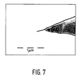
- Fig. 7 is a SEM photograph of part of an electron source according to a particular embodiment of the present invention.
- the photograph shows a substantially conical, point-shaped, tungsten tip electrode (on the right) to whose extremity an N-doped InAs nanowire has been Ohmically attached (center).
- the radius of the depicted nanowire is of the order of 30 nm, and its length is of the order of 2 ⁇ m (of which only a portion protrudes beyond the tip electrode).
- an electric potential of ca. 1.5 kV is applied to the tungsten electrode (at a temperature of 300K)
- electron emission with a very low energy spread ⁇ E occurs from the protruding extremity of the nanowire (i.e. remote from the tungsten tip).
- Fig. 8 shows a particle-optical apparatus in the form of an electron microscope.
- the apparatus includes an electron source 1, a beam alignment system 3 and a beam diaphragm 4, a condenser lens 6, an objective lens 8, a beam scanning system 10, an object space 11 with a specimen holder 13, a diffraction lens 12, an intermediate lens 14, a projection lens 16 and an electron detector 18.
- the objective lens 8, the intermediate lens 14 and the projection lens 16 together constitute an imaging lens system.
- These elements are accommodated in a housing provided with an electric supply lead 2 for the electron source, a viewing window 7 and a vacuum pumping device 17.
- the energizing coils for the objective lens 8 are connected to a control unit 15 that is arranged to control the energizing of the imaging lens system.
- the electron microscope also includes a recording unit with the electron detector 18, an image processing unit 5 and a video display 9 for observing the images formed.
- the particular apparatus depicted in Fig. 8 is a TEM.
- a typical accelerative voltage for a TEM is 300 kV, whereas a typical accelerative voltage for a SEM is 30 kV.
- This higher accelerative voltage for a TEM is necessary so as ensure that electrons in the electron beam are at least partially irradiated through the object to be investigated. To this end, it is also necessary that an object to be investigated using a TEM have a certain maximal thickness, which is normally around 100 nm.
- a hybrid alternative to a SEM or TEM is a Transmissive Scanning Electron Microscope (TSEM), in which, in a SEM environment (characterized by a relatively low accelerative voltage), an electron detection plate is provided under a sample on specimen holder 13, which plate allows an image of the sample to be obtained.
- TSEM Transmissive Scanning Electron Microscope
- the apparatus in Fig. 8 employs an electron source 1 according to the current invention, for example as described above in Embodiment 6.
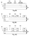
- Figure 9 shows a semiconductor wafer illuminated by an electron beam.
- a device 98 one or more electron sources according to the invention are used in an e-beam lithographic apparatus.
- the device may be an electric device such as an integrated circuit or a liquid crystal display device.
- a substrate 99 such as a semiconductor wafer 100, e.g. a monocrystalline silicon wafer, a silicon on insulator wafer or a GaAs wafer is provided.
- the substrate 99 may be a pre-fabricated integrated circuit and may comprise patterned and/or unpatterned layers 101 of other materials such as insulators, e.g. silicon dioxide, or electrical conductors, e.g. copper.
- the substrate 99 has a resist layer 102 having a solubility, which is alterable by electron bombardment. Any resist layer used for e-beam lithography may be used.
- the resist layer 102 is bombarded by electrons 104 extracted from an electron source according to the invention.
- the solubility of the resist layer 102 is locally altered.
- the resist layer thus obtained is developed thereby exposing a part 103 of the substrate 99 while a remainder of the substrate 99 remains being covered by a remainder 102' of the resist layer 102.
- the patterned resist layer 102' thus obtained is used as a mask in a material removal process such as a wet or a dry etching process, i.e. material of the substrate 99 exposed by the mask 102' is removed. In this way the substrate 99 is patterned.
- the substrate comprises two or more layers the upper layer 101 only, i.e. the layer close to the resist layer may be patterned in this way, resulting in a patterned layer 101'.
- a selective etching method may be used.
Landscapes
- Engineering & Computer Science (AREA)
- Chemical & Material Sciences (AREA)
- Nanotechnology (AREA)
- Physics & Mathematics (AREA)
- Mathematical Physics (AREA)
- Theoretical Computer Science (AREA)
- Crystallography & Structural Chemistry (AREA)
- Analytical Chemistry (AREA)
- Electron Sources, Ion Sources (AREA)
Priority Applications (1)
| Application Number | Priority Date | Filing Date | Title |
|---|---|---|---|
| EP05077145A EP1641012A3 (de) | 2004-09-24 | 2005-09-19 | Niedrige Energiespreizung Elektronenquelle |
Applications Claiming Priority (2)
| Application Number | Priority Date | Filing Date | Title |
|---|---|---|---|
| EP04077645 | 2004-09-24 | ||
| EP05077145A EP1641012A3 (de) | 2004-09-24 | 2005-09-19 | Niedrige Energiespreizung Elektronenquelle |
Publications (2)
| Publication Number | Publication Date |
|---|---|
| EP1641012A2 true EP1641012A2 (de) | 2006-03-29 |
| EP1641012A3 EP1641012A3 (de) | 2008-12-03 |
Family
ID=35533712
Family Applications (1)
| Application Number | Title | Priority Date | Filing Date |
|---|---|---|---|
| EP05077145A Withdrawn EP1641012A3 (de) | 2004-09-24 | 2005-09-19 | Niedrige Energiespreizung Elektronenquelle |
Country Status (1)
| Country | Link |
|---|---|
| EP (1) | EP1641012A3 (de) |
Family Cites Families (6)
| Publication number | Priority date | Publication date | Assignee | Title |
|---|---|---|---|---|
| US5362972A (en) * | 1990-04-20 | 1994-11-08 | Hitachi, Ltd. | Semiconductor device using whiskers |
| US5359257A (en) * | 1990-12-03 | 1994-10-25 | Bunch Kyle J | Ballistic electron, solid state cathode |
| JPH0574333A (ja) * | 1991-09-13 | 1993-03-26 | Fujitsu Ltd | 量子化電子線発生装置 |
| JPH08180824A (ja) * | 1994-12-22 | 1996-07-12 | Hitachi Ltd | 電子線源、その製造方法、電子線源装置及びそれを用いた電子線装置 |
| JPH09161660A (ja) * | 1995-12-06 | 1997-06-20 | Hitachi Ltd | 電子線源および電子線装置 |
| JP3832402B2 (ja) * | 2002-08-12 | 2006-10-11 | 株式会社日立製作所 | カーボンナノチューブを有する電子源とそれを用いた電子顕微鏡および電子線描画装置 |
-
2005
- 2005-09-19 EP EP05077145A patent/EP1641012A3/de not_active Withdrawn
Also Published As
| Publication number | Publication date |
|---|---|
| EP1641012A3 (de) | 2008-12-03 |
Similar Documents
| Publication | Publication Date | Title |
|---|---|---|
| Dong et al. | ZnO nanowires formed on tungsten substrates and their electron field emission properties | |
| JP3832402B2 (ja) | カーボンナノチューブを有する電子源とそれを用いた電子顕微鏡および電子線描画装置 | |
| EP1291889B1 (de) | Kohlenstofffasern verwendende Elektronenemittierende Vorrichtung; Elektronenquelle; Bildanzeigevorrichtung und Verfahren zur Herstellung | |
| US8952605B2 (en) | Metal hexaboride cold field emitter, method of fabricating same, and electron gun | |
| JP5636053B2 (ja) | ガス電界電離イオン源及びその使用方法、並びに、イオンビーム装置 | |
| CN109804450B (zh) | 电子束装置 | |
| US8764994B2 (en) | Method for fabricating emitter | |
| CN104425199A (zh) | 修正装置 | |
| EP4050637A1 (de) | Emitter, elektronenkanone mit verwendung davon, elektronische vorrichtung mit verwendung davon und verfahren zur herstellung davon | |
| EP2575158B1 (de) | Verfahren zum Herstellen einer Teilchenquelle | |
| JP4029289B2 (ja) | 導電性針の製造方法及びその方法により製造された導電性針 | |
| US7288773B2 (en) | Electron source, and charged-particle apparatus comprising such an electron source | |
| JP5564689B2 (ja) | 電界電離型ガスイオン源のエミッタおよびこれを備えた集束イオンビーム装置ならびに電界電離型ガスイオン源のエミッタの製造方法 | |
| EP1641012A2 (de) | Niedrige Energiespreizung Elektronenquelle | |
| JP3982558B2 (ja) | カーボンナノチューブを有する電子源とそれを用いた電子顕微鏡および電子線描画装置 | |
| da Silva Dantas et al. | ZnO Nanowire-Based Field Emission Devices Through a Microelectronic Compatible Route | |
| JP2007287401A (ja) | 導電性針およびその製造方法 | |
| KR102076956B1 (ko) | 표면산화막과 전계증발현상을 이용한 금속선 팁의 초미세 선단부 가공방법 | |
| Bischoff et al. | Nanostructures by mass-separated FIB | |
| Mäntynen | Doping of vapor–liquid–solid grown gallium arsenide nanowires | |
| EP1755137A1 (de) | Verfahren zur Herstellung eines Kohlenstoffnanoröhrenemitters, Kohlenstoffnanoröhrenemitter mit Anwendungen in Nanodruck und dessen Verwendung | |
| Fontana | Electron Microscopy-based Study of Nanostructured ZnO: Morphological, Structural and Electrical Characterization | |
| Yafarov et al. | Field Emission Properties of Nanostructured Silicon Cathode Arrays | |
| Perez | The Effects of Residual Gases on the Field Emission Properties of ZnO, GaN, ZnS Nanostructures, and the Effects of Light on the Resistivity of Graphene | |
| Eroles | Nanoetching and structural and electrical characterisation of cristalline graphene nanoribbons |
Legal Events
| Date | Code | Title | Description |
|---|---|---|---|
| PUAI | Public reference made under article 153(3) epc to a published international application that has entered the european phase |
Free format text: ORIGINAL CODE: 0009012 |
|
| 17P | Request for examination filed |
Effective date: 20050919 |
|
| AK | Designated contracting states |
Kind code of ref document: A2 Designated state(s): AT BE BG CH CY CZ DE DK EE ES FI FR GB GR HU IE IS IT LI LT LU LV MC NL PL PT RO SE SI SK TR |
|
| AX | Request for extension of the european patent |
Extension state: AL BA HR MK YU |
|
| PUAL | Search report despatched |
Free format text: ORIGINAL CODE: 0009013 |
|
| AK | Designated contracting states |
Kind code of ref document: A3 Designated state(s): AT BE BG CH CY CZ DE DK EE ES FI FR GB GR HU IE IS IT LI LT LU LV MC NL PL PT RO SE SI SK TR |
|
| AX | Request for extension of the european patent |
Extension state: AL BA HR MK YU |
|
| 17Q | First examination report despatched |
Effective date: 20090608 |
|
| AKX | Designation fees paid |
Designated state(s): DE FR GB |
|
| RBV | Designated contracting states (corrected) |
Designated state(s): AT BE BG CH CY CZ DE DK EE ES FI FR GB GR HU IE IS IT LI LT LU LV MC NL PL PT RO SE SI SK TR |
|
| RAP1 | Party data changed (applicant data changed or rights of an application transferred) |
Owner name: FEI COMPANY |
|
| STAA | Information on the status of an ep patent application or granted ep patent |
Free format text: STATUS: THE APPLICATION IS DEEMED TO BE WITHDRAWN |
|
| 18D | Application deemed to be withdrawn |
Effective date: 20110517 |