EP1641132A1 - Sender und Übertragungsverfahren - Google Patents
Sender und Übertragungsverfahren Download PDFInfo
- Publication number
- EP1641132A1 EP1641132A1 EP04360087A EP04360087A EP1641132A1 EP 1641132 A1 EP1641132 A1 EP 1641132A1 EP 04360087 A EP04360087 A EP 04360087A EP 04360087 A EP04360087 A EP 04360087A EP 1641132 A1 EP1641132 A1 EP 1641132A1
- Authority
- EP
- European Patent Office
- Prior art keywords
- signal
- adaptation
- frequency signal
- predistortion
- isr
- Prior art date
- Legal status (The legal status is an assumption and is not a legal conclusion. Google has not performed a legal analysis and makes no representation as to the accuracy of the status listed.)
- Granted
Links
- 230000005540 biological transmission Effects 0.000 title claims description 11
- 238000000034 method Methods 0.000 title claims description 11
- 230000006978 adaptation Effects 0.000 claims abstract description 35
- 238000012545 processing Methods 0.000 claims description 12
- 238000004590 computer program Methods 0.000 claims 1
- 238000005259 measurement Methods 0.000 description 12
- 238000004891 communication Methods 0.000 description 9
- 230000003044 adaptive effect Effects 0.000 description 4
- 235000000332 black box Nutrition 0.000 description 4
- 238000012549 training Methods 0.000 description 4
- 230000000694 effects Effects 0.000 description 3
- 238000013459 approach Methods 0.000 description 2
- 230000015556 catabolic process Effects 0.000 description 2
- 238000006243 chemical reaction Methods 0.000 description 2
- 238000012937 correction Methods 0.000 description 2
- 238000006731 degradation reaction Methods 0.000 description 2
- 238000010586 diagram Methods 0.000 description 2
- 238000006073 displacement reaction Methods 0.000 description 2
- 238000013139 quantization Methods 0.000 description 2
- 238000004088 simulation Methods 0.000 description 2
- 230000003595 spectral effect Effects 0.000 description 2
- 230000001629 suppression Effects 0.000 description 2
- 230000009897 systematic effect Effects 0.000 description 2
- 238000000342 Monte Carlo simulation Methods 0.000 description 1
- 230000009286 beneficial effect Effects 0.000 description 1
- 230000010267 cellular communication Effects 0.000 description 1
- 230000002301 combined effect Effects 0.000 description 1
- 230000003247 decreasing effect Effects 0.000 description 1
- 238000013461 design Methods 0.000 description 1
- 238000005516 engineering process Methods 0.000 description 1
- 238000001914 filtration Methods 0.000 description 1
- 238000005457 optimization Methods 0.000 description 1
- 230000010363 phase shift Effects 0.000 description 1
- 230000005855 radiation Effects 0.000 description 1
- 238000001228 spectrum Methods 0.000 description 1
- 230000009466 transformation Effects 0.000 description 1
- 238000000844 transformation Methods 0.000 description 1
Images




Classifications
-
- H—ELECTRICITY
- H04—ELECTRIC COMMUNICATION TECHNIQUE
- H04B—TRANSMISSION
- H04B1/00—Details of transmission systems, not covered by a single one of groups H04B3/00 - H04B13/00; Details of transmission systems not characterised by the medium used for transmission
- H04B1/02—Transmitters
- H04B1/04—Circuits
- H04B1/0475—Circuits with means for limiting noise, interference or distortion
-
- H—ELECTRICITY
- H03—ELECTRONIC CIRCUITRY
- H03F—AMPLIFIERS
- H03F1/00—Details of amplifiers with only discharge tubes, only semiconductor devices or only unspecified devices as amplifying elements
- H03F1/32—Modifications of amplifiers to reduce non-linear distortion
- H03F1/3241—Modifications of amplifiers to reduce non-linear distortion using predistortion circuits
-
- H—ELECTRICITY
- H04—ELECTRIC COMMUNICATION TECHNIQUE
- H04B—TRANSMISSION
- H04B1/00—Details of transmission systems, not covered by a single one of groups H04B3/00 - H04B13/00; Details of transmission systems not characterised by the medium used for transmission
- H04B1/02—Transmitters
- H04B1/04—Circuits
- H04B2001/0408—Circuits with power amplifiers
- H04B2001/0425—Circuits with power amplifiers with linearisation using predistortion
Definitions
- the present invention relates to the field of telecommunication, and more particularly to advanced transmitter architectures based on I/Q signal processing.
- the rejection of the image signal is a problem inherent to all receiver architectures.
- One of the benefits of a low-IF receiver is, that image rejection is realized by I/Q signal processing instead of a fixed analog filter, making it highly reconfigurable and cost-efficient.
- unavoidable imbalances between the land Q- branch leads to a limited image attenuation.
- the I/Q imbalance compensation can be realized in the digital part of the transmitter in terms of a digital pre-distortion.
- a proper calibration of the pre-distortion block with respect to the subsequent unknown I/Q imbalance is challenging. All previously published calibration techniques are performed offline using dedicated calibration signals (cf. J. K. Cavers and M. W. Liao, "Adaptive Compensation for Imbalance and Offset Losses in Direct Conversion Transceivers," IEEE Transactions on Vehicular Technology, vol. 42, pp. 581-588, Nov. 1993 and X. Huang and M. Caron, "Gain/phase imbalance and DC offset compensation in quadrature modulators," in IEEE International Symposium on Circuits and Systems 2002, vol. 4, pp. IV-811-IV-814, 26-29 May 2002).
- offline calibration requires an interrupt of the regular transmission mode.
- the signal path to the antenna has to be disconnected during calibration in order to prevent the calibration signal from being radiated.
- a transmitter has means for generating an intermediate frequency (IF) signal, means for predistortion of the IF signal using a predistortion parameter, means for generating a radio frequency (RF) signal from the predistorted (IF) signal, means for measuring an image-to-signal-ratio (ISR) of the RF signal, and means for adaptation of the predistortion parameter for reduction of the ISR.
- IF intermediate frequency
- RF radio frequency
- ISR image-to-signal-ratio
- the present invention is particularly advantageous as it enables on-line calibration of the predistortion parameters using the regular transmit signal only.
- the ISR is defined as the amplitude or power ratio of the image signal and the desired signal.
- the present invention can be used for uplink and/or for downlink transmitters.
- the invention can be implemented in a base station of a cellular communication network or in a mobile terminal, such as a mobile phone.
- the adaptation of the predistortion parameters is performed using an iterative algorithm.
- a cost function is used for the iterative procedure.
- the iterations serve to provide increasingly accurate estimates of the predistortion parameters and increasingly accurate approximations of the cost function.
- a feedback path from an RF part of the transmitter is realized on the basis of a heterodyne receiver architecture.
- the frequency of the analog down-mixing local oscillator and the frequency of the additional digital local oscillator is adjusted to the frequency of the transmit local oscillator.
- the power estimates for determining the ISR can be obtained using time averages of the corresponding baseband signals.
- the current ISR is compared with a threshold ISR.
- the threshold ISR is defined in a wireless communication standard that is to be implemented by the transmitter.
- the target ISR no further adaptation of the predistortion parameters is performed until the current ISR increases above the target ISR.
- the target ISR is chosen to be in compliance with the applicable standard.
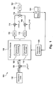
- Figure 1 shows a transmitter 100.
- the transmitter 100 has a digital-IF architecture.
- the upconversion of the transmit signal 102 from baseband to the RF carrier frequency is realized by a tuneable digital I/Q upconversion and a subsequent tuneable or fixed analog I/Q upconversion.
- the transmitter 100 has a digital mixer 104.
- the digital mixer 104 serves to generate an IF signal z from the baseband signal x.
- the IF signal z is received by a predistortion module 106.
- the predistortion module 106 has a predistortion processing component 108 for processing the lF signal z in order to compensate for hardware tolerances that cause the image signal.
- the predistortion module 106 has a storage 110 for storage of one or more predistortion parameters that are used by the predistortion processing component 108 in order to perform the predistortion processing of the IF signal z.
- the lF signal z is converted from digital to analog by the digital to analog converters 112.
- the I and Q components of the lF signal z are upconverted by multipliers 114 and 116, respectively.
- the upconverted I and Q components of the IF signal z are substracted by substractor 118 and the resultant radio frequency (RF) signal r is amplified by means of the power amplifier (PA) 120.
- the power amplifier 120 is coupled to an antenna 122 for sending of the power amplified RF signal r.
- the transmitter 100 has an image-to-signal-power-ratio (ISR) measurement component 124 for determining or estimating an ISR of the RF signal r.
- the ISR measurement component 124 provides the ISR to a parameter adaptation component 126 of the transmitter 100.
- the parameter adaptation component 126 implements an algorithm for calibrating the predistortion parameter(s) for reduction of the ISR.
- the adapted predistortion parameter(s) are provided from the parameter adaptation component 126 to the storage 110 for use by the predistortion processing component 108.
- the digital baseband signal x(kT) is considered as an exemplary transmit signal 102.
- ⁇ IF denotes the (angular) frequency of the digital mixer.
- LO analog local oscillator
- the RF signal consists of the desired transmit signal with the (angular) carrier frequency ⁇ LO + ⁇ IF , plus the unwanted image signal with the (angular) carrier frequency ⁇ LO - ⁇ IF .
- Each signal component is weighted by the I/Q imbalance parameters K 1 and K 2 , respectively.
- 2 is determined by the I/Q imbalance parameters only; it is independent from the transmit power P x itself.
- Figure 3 shows a preferred mode of operation of the transmitter 100 of figure 1 including predistortion processing and parameter adaptation for reduction of the ISR.
- the baseband signal x is provided.
- the baseband signal x is digitally I/Q mixed to provide the IF signal z.
- the IF signal z is processed in order to predistort the IF signal z using one of more predistortion parameters for reduction of the ISR of the RF signal r.
- the resultant predistorted IF signal z is multiplied by means of an analog oscillator to provide the RF signal r (step 306).
- the RF signal r is power amplified in step 308.
- the ISR of the RF signal r is measured or estimated.
- the current ISR is used in step 312 for adaptation of the predistortion parameters for reduction of the ISR. If the current ISR is already below a threshold or target ISR such further adaptation is not necessary.
- the I/Q imbalance compensation approach considered here is based on a digital pre-distortion.
- ⁇ and ⁇ are unknown, they have to be estimated. It is beneficial to perform the parameter estimation and the associated I/Q imbalance compensation blindly during regular operation of the transmitter as this avoids a need to feed the transmitter 100 with a dedicated training or calibration signal.
- the idea is to view the joint system of pre-distortion and real I/Q imbalance as a black-box with unknown parameters ⁇ , ⁇ inside.
- the input of the black-box is fed with known compensation parameters ⁇ , ⁇ resulting in an observable ISR at the output.
- By repeated reconfiguration of the pre-distortion a solution is found that leads to a sufficiently low ISR at the output.
- ISR P i P s
- This cost function alone does not provide sufficient information about the unknown I/Q imbalance parameters.
- J( ⁇ n , ⁇ m ) and J( ⁇ n -1, ⁇ m ) are known, which where gained using two different settings of ⁇ ,but two identical settings of ⁇ .
- ⁇ 1 2 [ ⁇ ⁇ m + ⁇ ⁇ m ⁇ 1 ⁇ J ( ⁇ ⁇ n , ⁇ ⁇ m ) ⁇ J ( ⁇ ⁇ n , ⁇ ⁇ m ⁇ 1 ) ⁇ ⁇ m ⁇ ⁇ ⁇ m ⁇ 1 ] .
- FIG. 7 A typical plot of the adaptation is shown in Fig. 7. Both the estimation errors and the measured ISR are shown in dB-scale:
- dB 20 log 10
- dB 20 log 10
- ISR dB 10 log 10 ISR
- Fig. 8 The result after 10.000 independent realizations is shown in Fig. 8. For each iteration the minimum, the maximum and the average ISR of all realizations is plotted. It can be seen, that the maximum (worst case) plot shows slightly higher ISR values than the exemplary plot in Fig. 7. This effect is a result of higher initial estimation errors in the case of a highly imbalanced analog mixer (
- the adaptation shows a random behavior. This is not critical, if the algorithm is used for an initial calibration of the transmitter only. In this case the adaptation can be stopped when a predefined target ISR, depending on the RF requirements of the chosen communications standard, is reached. However the algorithm can also be used for continuous adaptation, for example in order to track a time-variant I/Q imbalance.
- the adaptation of the digital pre-distortion block is performed during regular transmission mode without the need for any special calibration or training signal. Simulations have shown the rapid and reliable convergence of the estimated compensation parameters for arbitrary realistic I/Q imbalances.
- the present invention is particularly advantageous as the adaptation of the predistortion parameters can be performed blindly during regular transmission mode. With the proposed novel adaptation algorithm no special training or calibration signal is required.
Landscapes
- Engineering & Computer Science (AREA)
- Computer Networks & Wireless Communication (AREA)
- Signal Processing (AREA)
- Physics & Mathematics (AREA)
- Nonlinear Science (AREA)
- Power Engineering (AREA)
- Transmitters (AREA)
- Digital Transmission Methods That Use Modulated Carrier Waves (AREA)
- Radar Systems Or Details Thereof (AREA)
- Amplifiers (AREA)
- Amplitude Modulation (AREA)
Priority Applications (9)
| Application Number | Priority Date | Filing Date | Title |
|---|---|---|---|
| AT04360087T ATE365398T1 (de) | 2004-09-24 | 2004-09-24 | Sender und übertragungsverfahren |
| DE602004007136T DE602004007136T2 (de) | 2004-09-24 | 2004-09-24 | Sender und Übertragungsverfahren |
| EP04360087A EP1641132B8 (de) | 2004-09-24 | 2004-09-24 | Sender und Übertragungsverfahren |
| DE602004009182T DE602004009182T2 (de) | 2004-09-24 | 2004-11-10 | Digitale Seitenbandunterdrückung für Hochfrequenzmodulatoren |
| AT04292692T ATE374460T1 (de) | 2004-09-24 | 2004-11-10 | Digitale seitenbandunterdrückung für hochfrequenzmodulatoren |
| EP04292692A EP1641131B1 (de) | 2004-09-24 | 2004-11-10 | Digitale Seitenbandunterdrückung für Hochfrequenzmodulatoren |
| US11/209,670 US20060067425A1 (en) | 2004-09-24 | 2005-08-24 | Transmitter and transmission method |
| JP2005261674A JP4206090B2 (ja) | 2004-09-24 | 2005-09-09 | 送信機および送信方法 |
| CNB2005101028715A CN100459441C (zh) | 2004-09-24 | 2005-09-13 | 发射机和发送方法 |
Applications Claiming Priority (1)
| Application Number | Priority Date | Filing Date | Title |
|---|---|---|---|
| EP04360087A EP1641132B8 (de) | 2004-09-24 | 2004-09-24 | Sender und Übertragungsverfahren |
Publications (3)
| Publication Number | Publication Date |
|---|---|
| EP1641132A1 true EP1641132A1 (de) | 2006-03-29 |
| EP1641132B1 EP1641132B1 (de) | 2007-06-20 |
| EP1641132B8 EP1641132B8 (de) | 2007-09-05 |
Family
ID=34931522
Family Applications (2)
| Application Number | Title | Priority Date | Filing Date |
|---|---|---|---|
| EP04360087A Expired - Lifetime EP1641132B8 (de) | 2004-09-24 | 2004-09-24 | Sender und Übertragungsverfahren |
| EP04292692A Expired - Lifetime EP1641131B1 (de) | 2004-09-24 | 2004-11-10 | Digitale Seitenbandunterdrückung für Hochfrequenzmodulatoren |
Family Applications After (1)
| Application Number | Title | Priority Date | Filing Date |
|---|---|---|---|
| EP04292692A Expired - Lifetime EP1641131B1 (de) | 2004-09-24 | 2004-11-10 | Digitale Seitenbandunterdrückung für Hochfrequenzmodulatoren |
Country Status (6)
| Country | Link |
|---|---|
| US (1) | US20060067425A1 (de) |
| EP (2) | EP1641132B8 (de) |
| JP (1) | JP4206090B2 (de) |
| CN (1) | CN100459441C (de) |
| AT (2) | ATE365398T1 (de) |
| DE (2) | DE602004007136T2 (de) |
Families Citing this family (51)
| Publication number | Priority date | Publication date | Assignee | Title |
|---|---|---|---|---|
| US8145153B2 (en) * | 2006-09-20 | 2012-03-27 | Nxp B.V. | Method and system for calibrating an analogue I/Q-modulator of a transmitter |
| JP4866388B2 (ja) | 2008-05-22 | 2012-02-01 | 富士通株式会社 | 歪補償装置および歪補償方法 |
| US8854019B1 (en) | 2008-09-25 | 2014-10-07 | Rf Micro Devices, Inc. | Hybrid DC/DC power converter with charge-pump and buck converter |
| US9166471B1 (en) | 2009-03-13 | 2015-10-20 | Rf Micro Devices, Inc. | 3D frequency dithering for DC-to-DC converters used in multi-mode cellular transmitters |
| US8315576B2 (en) | 2009-05-05 | 2012-11-20 | Rf Micro Devices, Inc. | Capacitive compensation of cascaded directional couplers |
| US20120236964A1 (en) * | 2009-11-30 | 2012-09-20 | Dov Wulich | System and method for reducing bit-error-rate in orthogonal frequency-division multiplexing |
| US8670501B2 (en) | 2009-12-09 | 2014-03-11 | Texas Instruments Incorporated | Digital pre-distortion of non-linear systems with reduced bandwidth feedback |
| US8548398B2 (en) | 2010-02-01 | 2013-10-01 | Rf Micro Devices, Inc. | Envelope power supply calibration of a multi-mode radio frequency power amplifier |
| US8538355B2 (en) | 2010-04-19 | 2013-09-17 | Rf Micro Devices, Inc. | Quadrature power amplifier architecture |
| US8565694B2 (en) | 2010-04-20 | 2013-10-22 | Rf Micro Devices, Inc. | Split current current digital-to-analog converter (IDAC) for dynamic device switching (DDS) of an RF PA stage |
| US8542061B2 (en) | 2010-04-20 | 2013-09-24 | Rf Micro Devices, Inc. | Charge pump based power amplifier envelope power supply and bias power supply |
| US8913971B2 (en) | 2010-04-20 | 2014-12-16 | Rf Micro Devices, Inc. | Selecting PA bias levels of RF PA circuitry during a multislot burst |
| US8811920B2 (en) | 2010-04-20 | 2014-08-19 | Rf Micro Devices, Inc. | DC-DC converter semiconductor die structure |
| US8989685B2 (en) | 2010-04-20 | 2015-03-24 | Rf Micro Devices, Inc. | Look-up table based configuration of multi-mode multi-band radio frequency power amplifier circuitry |
| US8983410B2 (en) | 2010-04-20 | 2015-03-17 | Rf Micro Devices, Inc. | Configurable 2-wire/3-wire serial communications interface |
| US9553550B2 (en) | 2010-04-20 | 2017-01-24 | Qorvo Us, Inc. | Multiband RF switch ground isolation |
| US8942650B2 (en) | 2010-04-20 | 2015-01-27 | Rf Micro Devices, Inc. | RF PA linearity requirements based converter operating mode selection |
| US9362825B2 (en) | 2010-04-20 | 2016-06-07 | Rf Micro Devices, Inc. | Look-up table based configuration of a DC-DC converter |
| US8515361B2 (en) | 2010-04-20 | 2013-08-20 | Rf Micro Devices, Inc. | Frequency correction of a programmable frequency oscillator by propagation delay compensation |
| US8983407B2 (en) | 2010-04-20 | 2015-03-17 | Rf Micro Devices, Inc. | Selectable PA bias temperature compensation circuitry |
| US8811921B2 (en) | 2010-04-20 | 2014-08-19 | Rf Micro Devices, Inc. | Independent PA biasing of a driver stage and a final stage |
| US8958763B2 (en) | 2010-04-20 | 2015-02-17 | Rf Micro Devices, Inc. | PA bias power supply undershoot compensation |
| US9184701B2 (en) | 2010-04-20 | 2015-11-10 | Rf Micro Devices, Inc. | Snubber for a direct current (DC)-DC converter |
| US8571492B2 (en) | 2010-04-20 | 2013-10-29 | Rf Micro Devices, Inc. | DC-DC converter current sensing |
| US8942651B2 (en) | 2010-04-20 | 2015-01-27 | Rf Micro Devices, Inc. | Cascaded converged power amplifier |
| US9214865B2 (en) | 2010-04-20 | 2015-12-15 | Rf Micro Devices, Inc. | Voltage compatible charge pump buck and buck power supplies |
| US8706063B2 (en) | 2010-04-20 | 2014-04-22 | Rf Micro Devices, Inc. | PA envelope power supply undershoot compensation |
| US8731498B2 (en) | 2010-04-20 | 2014-05-20 | Rf Micro Devices, Inc. | Temperature correcting an envelope power supply signal for RF PA circuitry |
| US9577590B2 (en) | 2010-04-20 | 2017-02-21 | Qorvo Us, Inc. | Dual inductive element charge pump buck and buck power supplies |
| US9030256B2 (en) | 2010-04-20 | 2015-05-12 | Rf Micro Devices, Inc. | Overlay class F choke |
| US9077405B2 (en) | 2010-04-20 | 2015-07-07 | Rf Micro Devices, Inc. | High efficiency path based power amplifier circuitry |
| US9900204B2 (en) | 2010-04-20 | 2018-02-20 | Qorvo Us, Inc. | Multiple functional equivalence digital communications interface |
| US8559898B2 (en) | 2010-04-20 | 2013-10-15 | Rf Micro Devices, Inc. | Embedded RF PA temperature compensating bias transistor |
| US8699973B2 (en) | 2010-04-20 | 2014-04-15 | Rf Micro Devices, Inc. | PA bias power supply efficiency optimization |
| US9048787B2 (en) | 2010-04-20 | 2015-06-02 | Rf Micro Devices, Inc. | Combined RF detector and RF attenuator with concurrent outputs |
| US9214900B2 (en) * | 2010-04-20 | 2015-12-15 | Rf Micro Devices, Inc. | Interference reduction between RF communications bands |
| US8842399B2 (en) | 2010-04-20 | 2014-09-23 | Rf Micro Devices, Inc. | ESD protection of an RF PA semiconductor die using a PA controller semiconductor die |
| US8831544B2 (en) | 2010-04-20 | 2014-09-09 | Rf Micro Devices, Inc. | Dynamic device switching (DDS) of an in-phase RF PA stage and a quadrature-phase RF PA stage |
| US8913967B2 (en) | 2010-04-20 | 2014-12-16 | Rf Micro Devices, Inc. | Feedback based buck timing of a direct current (DC)-DC converter |
| US8947157B2 (en) | 2010-04-20 | 2015-02-03 | Rf Micro Devices, Inc. | Voltage multiplier charge pump buck |
| US9008597B2 (en) | 2010-04-20 | 2015-04-14 | Rf Micro Devices, Inc. | Direct current (DC)-DC converter having a multi-stage output filter |
| US8712349B2 (en) | 2010-04-20 | 2014-04-29 | Rf Micro Devices, Inc. | Selecting a converter operating mode of a PA envelope power supply |
| US8892063B2 (en) | 2010-04-20 | 2014-11-18 | Rf Micro Devices, Inc. | Linear mode and non-linear mode quadrature PA circuitry |
| US9479203B2 (en) * | 2011-04-14 | 2016-10-25 | Mediatek Inc. | Transceiver capable of IQ mismatch compensation on the fly and method thereof |
| US9065505B2 (en) | 2012-01-31 | 2015-06-23 | Rf Micro Devices, Inc. | Optimal switching frequency for envelope tracking power supply |
| US9998200B2 (en) | 2013-06-20 | 2018-06-12 | Aviat U.S., Inc. | Systems and methods for a fronthaul network |
| US11070416B2 (en) * | 2019-09-25 | 2021-07-20 | Apple Inc. | Time domain approach to determining a modulation or demodulation imbalance |
| JP7532795B2 (ja) * | 2020-02-12 | 2024-08-14 | 日本電気株式会社 | 光無線伝送システム |
| WO2022240975A1 (en) * | 2021-05-11 | 2022-11-17 | Analog Devices, Inc. | Enhanced dpd method to correct gain flatness for wireless communications systems |
| EP4199364A1 (de) | 2021-12-16 | 2023-06-21 | INTEL Corporation | Halbleiterbauelemente, sender-empfänger, basisstation und mobile vorrichtung |
| CN118041464B (zh) * | 2022-11-11 | 2025-12-19 | 中兴通讯股份有限公司 | 射频信号校正装置、方法及射频发射装置 |
Citations (2)
| Publication number | Priority date | Publication date | Assignee | Title |
|---|---|---|---|---|
| WO2003043206A2 (de) * | 2001-11-13 | 2003-05-22 | Infineon Technologies Ag | Sendeanordnung mit automatischem abgleich des quadraturmodulators |
| US6658065B1 (en) * | 2000-02-29 | 2003-12-02 | Skyworks Solutions, Inc. | System of and method for reducing or eliminating the unwanted sideband in the output of a transmitter comprising a quadrature modulator followed by a translational loop |
Family Cites Families (5)
| Publication number | Priority date | Publication date | Assignee | Title |
|---|---|---|---|---|
| IT1265271B1 (it) * | 1993-12-14 | 1996-10-31 | Alcatel Italia | Sistema di predistorsione in banda base per la linearizzazione adattativa di amplificatori di potenza |
| KR100255364B1 (ko) * | 1997-01-15 | 2000-05-01 | 윤종용 | 저주파신호 감쇄특성의 억제를 위한 무선수신기 및 그 억제방법 |
| US6298096B1 (en) * | 1998-11-19 | 2001-10-02 | Titan Corporation | Method and apparatus for determination of predistortion parameters for a quadrature modulator |
| EP1171984A1 (de) * | 1999-04-23 | 2002-01-16 | Nokia Corporation | Quadraturamplitudenmodulator |
| US6560449B1 (en) * | 2000-06-12 | 2003-05-06 | Broadcom Corporation | Image-rejection I/Q demodulators |
-
2004
- 2004-09-24 AT AT04360087T patent/ATE365398T1/de not_active IP Right Cessation
- 2004-09-24 DE DE602004007136T patent/DE602004007136T2/de not_active Expired - Lifetime
- 2004-09-24 EP EP04360087A patent/EP1641132B8/de not_active Expired - Lifetime
- 2004-11-10 AT AT04292692T patent/ATE374460T1/de not_active IP Right Cessation
- 2004-11-10 DE DE602004009182T patent/DE602004009182T2/de not_active Expired - Lifetime
- 2004-11-10 EP EP04292692A patent/EP1641131B1/de not_active Expired - Lifetime
-
2005
- 2005-08-24 US US11/209,670 patent/US20060067425A1/en not_active Abandoned
- 2005-09-09 JP JP2005261674A patent/JP4206090B2/ja not_active Expired - Fee Related
- 2005-09-13 CN CNB2005101028715A patent/CN100459441C/zh not_active Expired - Fee Related
Patent Citations (2)
| Publication number | Priority date | Publication date | Assignee | Title |
|---|---|---|---|---|
| US6658065B1 (en) * | 2000-02-29 | 2003-12-02 | Skyworks Solutions, Inc. | System of and method for reducing or eliminating the unwanted sideband in the output of a transmitter comprising a quadrature modulator followed by a translational loop |
| WO2003043206A2 (de) * | 2001-11-13 | 2003-05-22 | Infineon Technologies Ag | Sendeanordnung mit automatischem abgleich des quadraturmodulators |
Also Published As
| Publication number | Publication date |
|---|---|
| JP4206090B2 (ja) | 2009-01-07 |
| EP1641131B1 (de) | 2007-09-26 |
| ATE365398T1 (de) | 2007-07-15 |
| DE602004009182T2 (de) | 2008-07-03 |
| US20060067425A1 (en) | 2006-03-30 |
| DE602004007136T2 (de) | 2008-02-21 |
| CN1753317A (zh) | 2006-03-29 |
| DE602004009182D1 (de) | 2007-11-08 |
| JP2006094486A (ja) | 2006-04-06 |
| DE602004007136D1 (de) | 2007-08-02 |
| EP1641132B8 (de) | 2007-09-05 |
| EP1641132B1 (de) | 2007-06-20 |
| CN100459441C (zh) | 2009-02-04 |
| EP1641131A1 (de) | 2006-03-29 |
| ATE374460T1 (de) | 2007-10-15 |
Similar Documents
| Publication | Publication Date | Title |
|---|---|---|
| EP1641132B1 (de) | Sender und Übertragungsverfahren | |
| KR100539874B1 (ko) | 무선 송수신장치에서 자가 보상장치 및 방법 | |
| KR101196519B1 (ko) | 스퓨리어스 방사 상쇄 기능을 갖는 송신기, 무선 통신 장치, 및 스퓨리어스 방사 상쇄 방법 | |
| CN109818691B (zh) | 无线接收器的二阶截取点(ip2)校准的方法 | |
| Windisch et al. | Adaptive I/Q imbalance compensation in low-IF transmitter architectures | |
| KR100794983B1 (ko) | 캐리어 누설을 억제하는 방법 및 시스템 | |
| US20150350000A1 (en) | Calibration method and calibration apparatus for calibrating mismatch between first signal path and second signal path of transmitter/receiver | |
| CN107863988B (zh) | 计算发射路径和接收路径之间泄漏的方法和无线通信电路 | |
| EP1976213B1 (de) | Verfahren zur Kalibrierung nicht idealer Sende-/Empfangsanordnungen | |
| US11664906B2 (en) | Method for calibrating transmitter | |
| US8639197B2 (en) | Method and system to prevent harmonics from causing distortion in a communications system | |
| JPWO2006001184A1 (ja) | 確率密度関数で重み付けした積分処理を用いた線形性評価方法と、それを用いた回路シミュレータ、評価装置、通信回路、およびプログラム | |
| CN114726455A (zh) | 终端设备自校准方法及装置 | |
| KR20120112614A (ko) | 개선된 dc 오프셋 추정 | |
| CN116584046B (zh) | 无线电发射机以及用于其的方法和控制器 | |
| US20180269995A1 (en) | Phase Alignment Among Multiple Transmitters | |
| Narayanan et al. | A neural network-based DPD coefficient determination for PA linearization in 5G and beyond-5G mmWave systems | |
| Polak et al. | Influence of IQ-errors on DVB-T2 performance and its suppression by different methods | |
| CN115277342B (zh) | 发送器电路、补偿值校正装置与同相与正交不平衡补偿值校正方法 | |
| Benítez Martínez | Digital cancellation techniques for self-interference cancellation in full duplex transceivers and compensation of unwanted distortion in MIMO transmitters | |
| CN121000196A (zh) | 一种杂散消除电路、杂散消除方法和电子设备 | |
| CN121124837A (zh) | 一种零中频信号校准系统及方法 | |
| CN121690423A (zh) | 对超宽带系统进行iq不平衡校准的方法和系统、电子装置、计算机存储介质及程序产品 | |
| Hekkala et al. | Compensation of impairments in the radio over fiber infrastructure | |
| CN105765885A (zh) | 无线接收器的二阶截取点(ip2)校准 |
Legal Events
| Date | Code | Title | Description |
|---|---|---|---|
| PUAI | Public reference made under article 153(3) epc to a published international application that has entered the european phase |
Free format text: ORIGINAL CODE: 0009012 |
|
| AK | Designated contracting states |
Kind code of ref document: A1 Designated state(s): AT BE BG CH CY CZ DE DK EE ES FI FR GB GR HU IE IT LI LU MC NL PL PT RO SE SI SK TR |
|
| AX | Request for extension of the european patent |
Extension state: AL HR LT LV MK |
|
| 17P | Request for examination filed |
Effective date: 20060228 |
|
| AKX | Designation fees paid |
Designated state(s): AT BE BG CH CY CZ DE DK EE ES FI FR GB GR HU IE IT LI LU MC NL PL PT RO SE SI SK TR |
|
| GRAP | Despatch of communication of intention to grant a patent |
Free format text: ORIGINAL CODE: EPIDOSNIGR1 |
|
| RAP1 | Party data changed (applicant data changed or rights of an application transferred) |
Owner name: ALCATEL LUCENT |
|
| GRAS | Grant fee paid |
Free format text: ORIGINAL CODE: EPIDOSNIGR3 |
|
| GRAA | (expected) grant |
Free format text: ORIGINAL CODE: 0009210 |
|
| AK | Designated contracting states |
Kind code of ref document: B1 Designated state(s): AT BE BG CH CY CZ DE DK EE ES FI FR GB GR HU IE IT LI LU MC NL PL PT RO SE SI SK TR |
|
| PG25 | Lapsed in a contracting state [announced via postgrant information from national office to epo] |
Ref country code: LI Free format text: LAPSE BECAUSE OF FAILURE TO SUBMIT A TRANSLATION OF THE DESCRIPTION OR TO PAY THE FEE WITHIN THE PRESCRIBED TIME-LIMIT Effective date: 20070620 Ref country code: CH Free format text: LAPSE BECAUSE OF FAILURE TO SUBMIT A TRANSLATION OF THE DESCRIPTION OR TO PAY THE FEE WITHIN THE PRESCRIBED TIME-LIMIT Effective date: 20070620 |
|
| REG | Reference to a national code |
Ref country code: GB Ref legal event code: FG4D |
|
| REG | Reference to a national code |
Ref country code: CH Ref legal event code: EP |
|
| REG | Reference to a national code |
Ref country code: IE Ref legal event code: FG4D |
|
| REF | Corresponds to: |
Ref document number: 602004007136 Country of ref document: DE Date of ref document: 20070802 Kind code of ref document: P |
|
| PG25 | Lapsed in a contracting state [announced via postgrant information from national office to epo] |
Ref country code: SE Free format text: LAPSE BECAUSE OF FAILURE TO SUBMIT A TRANSLATION OF THE DESCRIPTION OR TO PAY THE FEE WITHIN THE PRESCRIBED TIME-LIMIT Effective date: 20070920 |
|
| ET | Fr: translation filed | ||
| PG25 | Lapsed in a contracting state [announced via postgrant information from national office to epo] |
Ref country code: AT Free format text: LAPSE BECAUSE OF FAILURE TO SUBMIT A TRANSLATION OF THE DESCRIPTION OR TO PAY THE FEE WITHIN THE PRESCRIBED TIME-LIMIT Effective date: 20070620 Ref country code: PL Free format text: LAPSE BECAUSE OF FAILURE TO SUBMIT A TRANSLATION OF THE DESCRIPTION OR TO PAY THE FEE WITHIN THE PRESCRIBED TIME-LIMIT Effective date: 20070620 |
|
| NLV1 | Nl: lapsed or annulled due to failure to fulfill the requirements of art. 29p and 29m of the patents act | ||
| REG | Reference to a national code |
Ref country code: CH Ref legal event code: PL |
|
| PG25 | Lapsed in a contracting state [announced via postgrant information from national office to epo] |
Ref country code: BE Free format text: LAPSE BECAUSE OF FAILURE TO SUBMIT A TRANSLATION OF THE DESCRIPTION OR TO PAY THE FEE WITHIN THE PRESCRIBED TIME-LIMIT Effective date: 20070620 |
|
| PG25 | Lapsed in a contracting state [announced via postgrant information from national office to epo] |
Ref country code: CZ Free format text: LAPSE BECAUSE OF FAILURE TO SUBMIT A TRANSLATION OF THE DESCRIPTION OR TO PAY THE FEE WITHIN THE PRESCRIBED TIME-LIMIT Effective date: 20070620 Ref country code: NL Free format text: LAPSE BECAUSE OF FAILURE TO SUBMIT A TRANSLATION OF THE DESCRIPTION OR TO PAY THE FEE WITHIN THE PRESCRIBED TIME-LIMIT Effective date: 20070620 Ref country code: BG Free format text: LAPSE BECAUSE OF FAILURE TO SUBMIT A TRANSLATION OF THE DESCRIPTION OR TO PAY THE FEE WITHIN THE PRESCRIBED TIME-LIMIT Effective date: 20070920 Ref country code: ES Free format text: LAPSE BECAUSE OF FAILURE TO SUBMIT A TRANSLATION OF THE DESCRIPTION OR TO PAY THE FEE WITHIN THE PRESCRIBED TIME-LIMIT Effective date: 20071001 Ref country code: PT Free format text: LAPSE BECAUSE OF FAILURE TO SUBMIT A TRANSLATION OF THE DESCRIPTION OR TO PAY THE FEE WITHIN THE PRESCRIBED TIME-LIMIT Effective date: 20071120 Ref country code: SI Free format text: LAPSE BECAUSE OF FAILURE TO SUBMIT A TRANSLATION OF THE DESCRIPTION OR TO PAY THE FEE WITHIN THE PRESCRIBED TIME-LIMIT Effective date: 20070620 |
|
| PG25 | Lapsed in a contracting state [announced via postgrant information from national office to epo] |
Ref country code: SK Free format text: LAPSE BECAUSE OF FAILURE TO SUBMIT A TRANSLATION OF THE DESCRIPTION OR TO PAY THE FEE WITHIN THE PRESCRIBED TIME-LIMIT Effective date: 20070620 |
|
| PLBE | No opposition filed within time limit |
Free format text: ORIGINAL CODE: 0009261 |
|
| STAA | Information on the status of an ep patent application or granted ep patent |
Free format text: STATUS: NO OPPOSITION FILED WITHIN TIME LIMIT |
|
| PG25 | Lapsed in a contracting state [announced via postgrant information from national office to epo] |
Ref country code: IT Free format text: LAPSE BECAUSE OF FAILURE TO SUBMIT A TRANSLATION OF THE DESCRIPTION OR TO PAY THE FEE WITHIN THE PRESCRIBED TIME-LIMIT Effective date: 20070620 Ref country code: MC Free format text: LAPSE BECAUSE OF NON-PAYMENT OF DUE FEES Effective date: 20070930 Ref country code: GR Free format text: LAPSE BECAUSE OF FAILURE TO SUBMIT A TRANSLATION OF THE DESCRIPTION OR TO PAY THE FEE WITHIN THE PRESCRIBED TIME-LIMIT Effective date: 20070921 Ref country code: DK Free format text: LAPSE BECAUSE OF FAILURE TO SUBMIT A TRANSLATION OF THE DESCRIPTION OR TO PAY THE FEE WITHIN THE PRESCRIBED TIME-LIMIT Effective date: 20070620 |
|
| 26N | No opposition filed |
Effective date: 20080325 |
|
| PG25 | Lapsed in a contracting state [announced via postgrant information from national office to epo] |
Ref country code: RO Free format text: LAPSE BECAUSE OF FAILURE TO SUBMIT A TRANSLATION OF THE DESCRIPTION OR TO PAY THE FEE WITHIN THE PRESCRIBED TIME-LIMIT Effective date: 20070620 |
|
| PG25 | Lapsed in a contracting state [announced via postgrant information from national office to epo] |
Ref country code: IE Free format text: LAPSE BECAUSE OF NON-PAYMENT OF DUE FEES Effective date: 20070924 |
|
| PG25 | Lapsed in a contracting state [announced via postgrant information from national office to epo] |
Ref country code: EE Free format text: LAPSE BECAUSE OF FAILURE TO SUBMIT A TRANSLATION OF THE DESCRIPTION OR TO PAY THE FEE WITHIN THE PRESCRIBED TIME-LIMIT Effective date: 20070620 |
|
| PG25 | Lapsed in a contracting state [announced via postgrant information from national office to epo] |
Ref country code: FI Free format text: LAPSE BECAUSE OF FAILURE TO SUBMIT A TRANSLATION OF THE DESCRIPTION OR TO PAY THE FEE WITHIN THE PRESCRIBED TIME-LIMIT Effective date: 20070620 |
|
| PG25 | Lapsed in a contracting state [announced via postgrant information from national office to epo] |
Ref country code: CY Free format text: LAPSE BECAUSE OF FAILURE TO SUBMIT A TRANSLATION OF THE DESCRIPTION OR TO PAY THE FEE WITHIN THE PRESCRIBED TIME-LIMIT Effective date: 20070620 |
|
| PG25 | Lapsed in a contracting state [announced via postgrant information from national office to epo] |
Ref country code: LU Free format text: LAPSE BECAUSE OF NON-PAYMENT OF DUE FEES Effective date: 20070924 |
|
| PG25 | Lapsed in a contracting state [announced via postgrant information from national office to epo] |
Ref country code: HU Free format text: LAPSE BECAUSE OF FAILURE TO SUBMIT A TRANSLATION OF THE DESCRIPTION OR TO PAY THE FEE WITHIN THE PRESCRIBED TIME-LIMIT Effective date: 20071221 Ref country code: TR Free format text: LAPSE BECAUSE OF FAILURE TO SUBMIT A TRANSLATION OF THE DESCRIPTION OR TO PAY THE FEE WITHIN THE PRESCRIBED TIME-LIMIT Effective date: 20070620 |
|
| PGFP | Annual fee paid to national office [announced via postgrant information from national office to epo] |
Ref country code: FR Payment date: 20101005 Year of fee payment: 7 |
|
| PGFP | Annual fee paid to national office [announced via postgrant information from national office to epo] |
Ref country code: GB Payment date: 20100921 Year of fee payment: 7 |
|
| PGFP | Annual fee paid to national office [announced via postgrant information from national office to epo] |
Ref country code: DE Payment date: 20100922 Year of fee payment: 7 |
|
| GBPC | Gb: european patent ceased through non-payment of renewal fee |
Effective date: 20110924 |
|
| REG | Reference to a national code |
Ref country code: FR Ref legal event code: ST Effective date: 20120531 |
|
| REG | Reference to a national code |
Ref country code: DE Ref legal event code: R119 Ref document number: 602004007136 Country of ref document: DE Effective date: 20120403 |
|
| PG25 | Lapsed in a contracting state [announced via postgrant information from national office to epo] |
Ref country code: DE Free format text: LAPSE BECAUSE OF NON-PAYMENT OF DUE FEES Effective date: 20120403 |
|
| PG25 | Lapsed in a contracting state [announced via postgrant information from national office to epo] |
Ref country code: GB Free format text: LAPSE BECAUSE OF NON-PAYMENT OF DUE FEES Effective date: 20110924 Ref country code: FR Free format text: LAPSE BECAUSE OF NON-PAYMENT OF DUE FEES Effective date: 20110930 |
|
| REG | Reference to a national code |
Ref country code: FR Ref legal event code: CA Effective date: 20150521 |
|
| REG | Reference to a national code |
Ref country code: FR Ref legal event code: CA Effective date: 20150521 |