EP1643005A2 - Procédé de déposition de nanocouches inorganiques et/ou organiques par decharge de plasma - Google Patents
Procédé de déposition de nanocouches inorganiques et/ou organiques par decharge de plasma Download PDFInfo
- Publication number
- EP1643005A2 EP1643005A2 EP05405482A EP05405482A EP1643005A2 EP 1643005 A2 EP1643005 A2 EP 1643005A2 EP 05405482 A EP05405482 A EP 05405482A EP 05405482 A EP05405482 A EP 05405482A EP 1643005 A2 EP1643005 A2 EP 1643005A2
- Authority
- EP
- European Patent Office
- Prior art keywords
- plasma
- zone
- substrate
- reactor
- dye
- Prior art date
- Legal status (The legal status is an assumption and is not a legal conclusion. Google has not performed a legal analysis and makes no representation as to the accuracy of the status listed.)
- Withdrawn
Links
Images

Classifications
-
- C—CHEMISTRY; METALLURGY
- C23—COATING METALLIC MATERIAL; COATING MATERIAL WITH METALLIC MATERIAL; CHEMICAL SURFACE TREATMENT; DIFFUSION TREATMENT OF METALLIC MATERIAL; COATING BY VACUUM EVAPORATION, BY SPUTTERING, BY ION IMPLANTATION OR BY CHEMICAL VAPOUR DEPOSITION, IN GENERAL; INHIBITING CORROSION OF METALLIC MATERIAL OR INCRUSTATION IN GENERAL
- C23C—COATING METALLIC MATERIAL; COATING MATERIAL WITH METALLIC MATERIAL; SURFACE TREATMENT OF METALLIC MATERIAL BY DIFFUSION INTO THE SURFACE, BY CHEMICAL CONVERSION OR SUBSTITUTION; COATING BY VACUUM EVAPORATION, BY SPUTTERING, BY ION IMPLANTATION OR BY CHEMICAL VAPOUR DEPOSITION, IN GENERAL
- C23C16/00—Chemical coating by decomposition of gaseous compounds, without leaving reaction products of surface material in the coating, i.e. chemical vapour deposition [CVD] processes
- C23C16/006—Chemical coating by decomposition of gaseous compounds, without leaving reaction products of surface material in the coating, i.e. chemical vapour deposition [CVD] processes characterized by the colour of the layer
-
- B—PERFORMING OPERATIONS; TRANSPORTING
- B05—SPRAYING OR ATOMISING IN GENERAL; APPLYING FLUENT MATERIALS TO SURFACES, IN GENERAL
- B05D—PROCESSES FOR APPLYING FLUENT MATERIALS TO SURFACES, IN GENERAL
- B05D1/00—Processes for applying liquids or other fluent materials
- B05D1/62—Plasma-deposition of organic layers
-
- C—CHEMISTRY; METALLURGY
- C23—COATING METALLIC MATERIAL; COATING MATERIAL WITH METALLIC MATERIAL; CHEMICAL SURFACE TREATMENT; DIFFUSION TREATMENT OF METALLIC MATERIAL; COATING BY VACUUM EVAPORATION, BY SPUTTERING, BY ION IMPLANTATION OR BY CHEMICAL VAPOUR DEPOSITION, IN GENERAL; INHIBITING CORROSION OF METALLIC MATERIAL OR INCRUSTATION IN GENERAL
- C23C—COATING METALLIC MATERIAL; COATING MATERIAL WITH METALLIC MATERIAL; SURFACE TREATMENT OF METALLIC MATERIAL BY DIFFUSION INTO THE SURFACE, BY CHEMICAL CONVERSION OR SUBSTITUTION; COATING BY VACUUM EVAPORATION, BY SPUTTERING, BY ION IMPLANTATION OR BY CHEMICAL VAPOUR DEPOSITION, IN GENERAL
- C23C16/00—Chemical coating by decomposition of gaseous compounds, without leaving reaction products of surface material in the coating, i.e. chemical vapour deposition [CVD] processes
- C23C16/22—Chemical coating by decomposition of gaseous compounds, without leaving reaction products of surface material in the coating, i.e. chemical vapour deposition [CVD] processes characterised by the deposition of inorganic material, other than metallic material
- C23C16/30—Deposition of compounds, mixtures or solid solutions, e.g. borides, carbides, nitrides
-
- C—CHEMISTRY; METALLURGY
- C23—COATING METALLIC MATERIAL; COATING MATERIAL WITH METALLIC MATERIAL; CHEMICAL SURFACE TREATMENT; DIFFUSION TREATMENT OF METALLIC MATERIAL; COATING BY VACUUM EVAPORATION, BY SPUTTERING, BY ION IMPLANTATION OR BY CHEMICAL VAPOUR DEPOSITION, IN GENERAL; INHIBITING CORROSION OF METALLIC MATERIAL OR INCRUSTATION IN GENERAL
- C23C—COATING METALLIC MATERIAL; COATING MATERIAL WITH METALLIC MATERIAL; SURFACE TREATMENT OF METALLIC MATERIAL BY DIFFUSION INTO THE SURFACE, BY CHEMICAL CONVERSION OR SUBSTITUTION; COATING BY VACUUM EVAPORATION, BY SPUTTERING, BY ION IMPLANTATION OR BY CHEMICAL VAPOUR DEPOSITION, IN GENERAL
- C23C16/00—Chemical coating by decomposition of gaseous compounds, without leaving reaction products of surface material in the coating, i.e. chemical vapour deposition [CVD] processes
- C23C16/44—Chemical coating by decomposition of gaseous compounds, without leaving reaction products of surface material in the coating, i.e. chemical vapour deposition [CVD] processes characterised by the method of coating
- C23C16/448—Chemical coating by decomposition of gaseous compounds, without leaving reaction products of surface material in the coating, i.e. chemical vapour deposition [CVD] processes characterised by the method of coating characterised by the method used for generating reactive gas streams, e.g. by evaporation or sublimation of precursor materials
- C23C16/452—Chemical coating by decomposition of gaseous compounds, without leaving reaction products of surface material in the coating, i.e. chemical vapour deposition [CVD] processes characterised by the method of coating characterised by the method used for generating reactive gas streams, e.g. by evaporation or sublimation of precursor materials by activating reactive gas streams before their introduction into the reaction chamber, e.g. by ionisation or addition of reactive species
-
- H—ELECTRICITY
- H01—ELECTRIC ELEMENTS
- H01J—ELECTRIC DISCHARGE TUBES OR DISCHARGE LAMPS
- H01J37/00—Discharge tubes with provision for introducing objects or material to be exposed to the discharge, e.g. for the purpose of examination or processing thereof
- H01J37/32—Gas-filled discharge tubes
- H01J37/32431—Constructional details of the reactor
- H01J37/3266—Magnetic control means
-
- B—PERFORMING OPERATIONS; TRANSPORTING
- B05—SPRAYING OR ATOMISING IN GENERAL; APPLYING FLUENT MATERIALS TO SURFACES, IN GENERAL
- B05D—PROCESSES FOR APPLYING FLUENT MATERIALS TO SURFACES, IN GENERAL
- B05D5/00—Processes for applying liquids or other fluent materials to surfaces to obtain special surface effects, finishes or structures
- B05D5/06—Processes for applying liquids or other fluent materials to surfaces to obtain special surface effects, finishes or structures to obtain multicolour or other optical effects
Definitions
- the invention relates to a method for depositing organic and / or inorganic nanolayers on a substrate by means of plasma discharge, in particular by means of plasma-assisted chemical vapor deposition in a high-vacuum reactor. Furthermore, the invention relates to applications of the method.
- organic plasma-reactive materials are ethylene, isopropanol, butyl acrylate, butylene-1, ethyl acrylate, vinyl fluoride, vinyl chloride, vinyl alcohol, isobutyl methacrylate, hydroxyethyl acrylate, acylonitride, methyl methacrylate and styrene. This list of layer-forming monomers can be extended as desired.
- the monomers can be introduced into the reactor with or without carrier gas.
- an inert gas is preferably introduced, which also facilitates the ignition of the plasma and increases its stability. This applies in particular to the introduction of the noble gases argon, neon and helium.
- metal halides in practice fluorides and chlorides, hydrides or organometallic components are used as the layer-forming gaseous component.
- metals are aluminum, titanium and tungsten, as well as the semi-metals boron and silicon.
- a reactive gas is additionally supplied, for example oxygen or nitrogen, but also carbon monoxide, Carbon dioxide, hydrogen and / or ammonia.
- PECVD Plasma-enhanced chemical vapor deposition from a vapor phase
- the deposited organic layers usually have no or only a pale coloration, which is perceived as a defect for many applications. It is known, together with plasma-polymerizable monomers and possibly an inert gas, to introduce dye particles into the reaction zone which give the deposited layer the desired color effect. These particles are usually inorganic and opaque, for example metal particles.
- the inventors have set themselves the task of providing a method of the type mentioned, which allows an improved deposition of colored organic and / or inorganic nanolayers on a substrate by means of plasma discharge.
- the dyes should not be impaired in any way, and moreover, a simple and inexpensive process should be able to be carried out. Furthermore, a wide range of applications of the method will be opened.
- the object is achieved according to the invention that after evacuating the reactor at least one component of the group consisting of at least one each layer-forming monomer, a reactive gas and a carrier or inert gas, in the excitation zone for the plasma and at the same time dye molecules and / or submicron dye pigments in one of the excitation zone for the plasma spatially separated, lying outside the excitation zone diffusion zone in the region of the substrate and incorporated without agglomeration in the nano-layer.
- a reactive gas In the plasma polymerization of organic monomers, the supply of a reactive gas may be unnecessary, if it is a pure concatenation or crosslinking of molecular chains, d. H. without a chemical reaction taking place at the same time.
- a reactive gas For the production of inorganic nanolayers a reactive gas is always necessary.
- a carrier or inert gas, in particular a noble gas, can be introduced into the excitation zone alone, nanoparticles with outstanding optical properties being achieved with polymerizable dye molecules.
- an inert gas is preferably introduced into the evacuated reactor, which acts as a carrier gas for the ignition and the Increased stability of the plasma.
- Suitable inert gases are, as is known, primarily noble gases, in particular argon, neon and / or helium.
- hydrocarbons, including substituted ones, and silanes are primarily used as layer-forming monomers, it also being possible for the silanes to form inorganic layers, in particular silicon dioxide, SiO 2 .
- layer-forming monomers is also used here for metal-containing components, in particular metal halides and metal hydrides, organometallic compounds which form inorganic layers with the aid of reactive gases. In this case, one speaks of PECVD reactions, plasma-enhanced chemical deposits from the gas or vapor phase. The most common metal compounds used as layer-forming monomers are mentioned in the introduction to the description.
- the spectrum of usable dye molecules is large, thanks to the low temperature in the diffusion zone, preferably room temperature, the properties of the dye molecules remain unchanged.
- rhodamine 6G, auramine O, erytrosine B, methylene blue, metanil yellow, Congo Red and / or Nile Blue A are passed into the diffusion zone.
- the dye molecules can be added to the deposition process in the diffusion zone by sublimation from the outside via a gas line or in the reactor from an evaporator.
- the dye molecules are homogeneously distributed in the nanolayer.
- submicron dye pigments can be added to the diffusion zone as an alternative or in addition to the dye molecules and deposited together with the layer-forming monomers to form the nano-layer.
- the dye pigments are homogeneously distributed, no agglomeration is formed.
- virtually all known dye pigments are suitable, for example oxides, sulfates, silicates and chromates, in particular of tin, lead, zinc, titanium, barium, calcium and / or magnesium.
- the largest grain diameter of the dye pigments should be substantially below the thickness of the deposited nano-layer, preferably below 50%.
- the dye pigments are passed in an inert carrier gas into the diffusion zone.
- the structure and the color intensity of the deposited nanolayer can be controlled in a manner known per se by the flow of the layer-forming monomers, the reactive gases possibly supplied, the dye molecules and / or the dye pigments.
- At least partially fluorescent dye molecules and / or dye pigments can be introduced into the diffusion zone of the reactor.
- All substrates used in plasma technology with a diffusion zone located at room temperature are also suitable for carrying out the present invention. This applies both to the shape and the material.
- the substrate may be fixedly mounted as a plate or shaped body on a substrate holder or formed as an endlessly passing member in the form of a band, a string, a thread or the like.
- All customary substrate materials are suitable, for example polymeric plastics, textiles, ceramic materials, glass, various metals, in particular steel, aluminum, copper and brass, and semiconductors, in particular silicon, III-V semiconductors, such as eg. GaAs, and II-VI semiconductors such. ZnS.
- All the high-vacuum reactors used in plasma technology in which the excitation or reaction zone on the one hand and the diffusion zone with the substrate on the other hand are spatially clearly separated, are suitable for carrying out the process.
- the building materials, the energy supply, the supply of starting materials, the measuring and analysis devices, the high-vacuum reactor used for carrying out the method according to the invention has no fundamental differences.
- the present reactor type is also called "remote plant”. Preference is given to electrodeless reactors, in particular for the generation of an induced radio-wave (RF) or microwave plasma.
- RF radio-wave
- the wavelength ⁇ of microwaves is in the range of 10 -2 to 1 m, of radio waves in the range of 1 to 10 4 m.
- the deposition by means of a microwave plasma is preferably carried out with a power of 10 to 1000 watts, in particular from 50 to 200 watts.
- a vacuum of at least 10 -6 mbar can be generated, which is why this is referred to as a high vacuum reactor.
- the reactor is evacuated to about 10 -6 mbar.
- a working pressure in the range of 10 -2 to 10 mbar is maintained.
- the application possibilities of the method according to the invention are extremely diverse, they are predominantly in the field of coating of microelectronic components and the coating of textiles or as a layer for optoelectronic applications.
- Specific applications of the method are, for example, the production of waveguides for laser matrices, optical gas sensors, radiation detectors, electroluminescent devices, light-emitting diodes and measuring devices for the radioactivity.
- nano layers can be produced with the method according to the invention, into which dye molecules and / or dye pigments can be incorporated without changing their color spectrum. This is done in a simple and economical way.
- a high vacuum reactor is evacuated to a pressure of 10 -6 mbar. After reaching and maintaining this base pressure for a few minutes, the carrier gas is supplied with argon having a gas flow of 3 sccm. After the ignition of the plasma, Si (CH 3 ) 4 having a gas flow of 1 sccm and as reactive gas O 2 having a gas flow of likewise 1 sccm is fed as the layer-forming monomer. The working pressure is increased to 2 x 10 -2 mbar.
- the microwave power of the electrodeless high vacuum reactor is 100 watts.
- Dye molecules of rhodamine 6G are introduced into the diffusion zone of the reactor, which is separate from the plasma, and are precipitated together with the layer-forming monomer to form a red-colored SiO 2 layer at about 50 nm.
- a plasma is formed in the excitation zone.
- a layer-forming monomer isopropanol is introduced with a gas flow of 1 sccm, a reactive gas is not necessary.
- a working pressure of 10 -2 mbar and a microwave power of 100 watts rhodamine 6G is again supplied in molecular form in the diffusion zone.
- An approximately 25 nm thick red-colored plastic layer is formed on the substrate after 30 seconds.
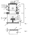
- a high-vacuum reactor 10 shown in FIG. 1 is substantially cylindrical in shape and comprises a smaller cross-sectional upper part 12 with a plasma source and a lower part 14 with a substrate 16, in the present case a glass plate.
- the two parts 12, 14 of the high vacuum reactor 10 are screwed together via flanges 18, 20 vacuum-tight.
- the high vacuum reactor 10 consists essentially of stainless steel and has the requirements corresponding to large wall thicknesses.
- a mild steel yoke 23 connects the two magnetic rings 22, so that a best possible magnetic flux is achieved.
- An ignited plasma 24, in this case an ECR (ECR Electron Cyclotron Resonance) plasma, fills the upper part 12 of the high-vacuum reactor 10, forming an excitation or reaction zone 26 inside the ring 22.
- ECR Electron
- microwaves 28 of a frequency f from the present 2.45 GHz characterized by arrows are directed via a window 30 in the reactor cover 32 into the interior of the upper part 12.
- an axially opening into the interior of the upper part 12 pipe socket 34 is formed, which in turn each has an inlet for inert gas or carrier gas 36, layer-forming monomers 38 and reactive gas 40.
- Carrier gas 36 and layer forming monomers 38 may also be previously mixed.
- the reactive gas inlet 40 is closed when none is necessary. Alternatively, three directly into the interior of the upper part 12 leading pipe socket 34 may be formed.
- the lower part 14 of the high-vacuum reactor 10 comprises a substrate holder 42 with the substrate 16, wherein a height-adjustable substrate carrier 44 is provided. Via a pipe socket 46, external dye molecules 48, according to a variant dye pigments 50, are guided into a diffusion zone 52 of the lower part 14, where room temperature prevails.
- a carrier or inert gas 36 is also used for the supply of dye molecules 48 or dye pigments 50.
- the gaseous phase is sucked off by a vacuum pump, not shown.
- the layer-forming monomers 38 or their reaction products from the excitation or reaction zone 26 are deposited together with the dye molecules 48 and / or Fabstoffpigmenten 50 as a colored nano-layer 56.
- a deposited nanosheet 56 having a thickness d of 50 nm is shown in FIG. 2 as being greatly exaggerated with respect to the substrate 16. Further, for the sake of clarity, all of the dye pigments 50 detected by the cutting plane have the same size. Dye molecules 48 are equivalently incorporated into the nanosheet 56 of 50 nm in thickness.
- the ECR plasma source may be formed differently depending on the type of excitation of the plasma 24 in the excitation zone 26, z.
- a microwave plasma source without magnets or inductively coupled RF plasma source.
- the magnets 22 and the mild steel yokes 23 form twelve magnetic shoes circumferentially around the circumference of the upper part 12 of the reactor 10, the more regularly arranged the better. All magnetic shoes have the same orientation in the arrangement according to FIG. 3, so that an inhomogeneous magnetic field which is toroidal in the interior builds up.
- the magnetic field strength of the permanent magnets must be selected be that the inhomogeneous magnetic field in the interior in some places has a field strength that is required for the ECR condition. For a microwave frequency of 2.45 GHz, this is 875 milliTesla (mT). For other microwave frequencies, correspondingly different field strengths result.
Landscapes
- Chemical & Material Sciences (AREA)
- Engineering & Computer Science (AREA)
- Materials Engineering (AREA)
- General Chemical & Material Sciences (AREA)
- Chemical Kinetics & Catalysis (AREA)
- Mechanical Engineering (AREA)
- Metallurgy (AREA)
- Organic Chemistry (AREA)
- Plasma & Fusion (AREA)
- Physics & Mathematics (AREA)
- Analytical Chemistry (AREA)
- Inorganic Chemistry (AREA)
- Chemical Vapour Deposition (AREA)
- Chemical Or Physical Treatment Of Fibers (AREA)
- Physical Vapour Deposition (AREA)
Applications Claiming Priority (1)
| Application Number | Priority Date | Filing Date | Title |
|---|---|---|---|
| CH14382004 | 2004-09-01 |
Publications (2)
| Publication Number | Publication Date |
|---|---|
| EP1643005A2 true EP1643005A2 (fr) | 2006-04-05 |
| EP1643005A3 EP1643005A3 (fr) | 2008-03-19 |
Family
ID=35731097
Family Applications (1)
| Application Number | Title | Priority Date | Filing Date |
|---|---|---|---|
| EP05405482A Withdrawn EP1643005A3 (fr) | 2004-09-01 | 2005-08-17 | Procédé de déposition de nanocouches inorganiques et/ou organiques par decharge de plasma |
Country Status (1)
| Country | Link |
|---|---|
| EP (1) | EP1643005A3 (fr) |
Cited By (7)
| Publication number | Priority date | Publication date | Assignee | Title |
|---|---|---|---|---|
| WO2009010753A3 (fr) * | 2007-07-17 | 2009-06-11 | P2I Ltd | Appareil de dépôt par plasma |
| EP2369032A1 (fr) * | 2010-03-25 | 2011-09-28 | Odelo GmbH | Procédé de fabrication de surfaces colorées |
| WO2012007388A1 (fr) * | 2010-07-12 | 2012-01-19 | Solvay Sa | Procédé de dépôt plasma de polymère |
| EP2666544A1 (fr) | 2012-05-24 | 2013-11-27 | Vito NV | Procédé pour le dépôt et la caractérisation d'un revêtement |
| US8852693B2 (en) | 2011-05-19 | 2014-10-07 | Liquipel Ip Llc | Coated electronic devices and associated methods |
| EP3722500A1 (fr) * | 2013-12-13 | 2020-10-14 | The North Face Apparel Corp. | Traitements par plasma pour la coloration de textiles |
| WO2023185465A1 (fr) * | 2022-03-29 | 2023-10-05 | 江苏菲沃泰纳米科技股份有限公司 | Revêtement hydrophile, procédé de préparation, et dispositif |
Family Cites Families (4)
| Publication number | Priority date | Publication date | Assignee | Title |
|---|---|---|---|---|
| DE19824364A1 (de) * | 1998-05-30 | 1999-12-02 | Bosch Gmbh Robert | Verfahren zum Aufbringen eines Verschleißschutz-Schichtsystems mit optischen Eigenschaften auf Oberflächen |
| ATE269172T1 (de) * | 2000-01-27 | 2004-07-15 | Incoat Gmbh | Schutz- und/oder diffusionssperrschicht |
| DE10104611A1 (de) * | 2001-02-02 | 2002-08-14 | Bosch Gmbh Robert | Vorrichtung zur keramikartigen Beschichtung eines Substrates |
| EP1581347B1 (fr) * | 2002-12-17 | 2009-02-25 | Wipf AG | Substrat enduit d'une couche polaire a polymerisation plasma |
-
2005
- 2005-08-17 EP EP05405482A patent/EP1643005A3/fr not_active Withdrawn
Cited By (9)
| Publication number | Priority date | Publication date | Assignee | Title |
|---|---|---|---|---|
| WO2009010753A3 (fr) * | 2007-07-17 | 2009-06-11 | P2I Ltd | Appareil de dépôt par plasma |
| GB2463427A (en) * | 2007-07-17 | 2010-03-17 | P2I Ltd | Plasma depositon apparatus |
| EP2369032A1 (fr) * | 2010-03-25 | 2011-09-28 | Odelo GmbH | Procédé de fabrication de surfaces colorées |
| WO2012007388A1 (fr) * | 2010-07-12 | 2012-01-19 | Solvay Sa | Procédé de dépôt plasma de polymère |
| US8852693B2 (en) | 2011-05-19 | 2014-10-07 | Liquipel Ip Llc | Coated electronic devices and associated methods |
| EP2666544A1 (fr) | 2012-05-24 | 2013-11-27 | Vito NV | Procédé pour le dépôt et la caractérisation d'un revêtement |
| US8927052B2 (en) | 2012-05-24 | 2015-01-06 | Vito Nv | Process for deposition and characterization of a coating |
| EP3722500A1 (fr) * | 2013-12-13 | 2020-10-14 | The North Face Apparel Corp. | Traitements par plasma pour la coloration de textiles |
| WO2023185465A1 (fr) * | 2022-03-29 | 2023-10-05 | 江苏菲沃泰纳米科技股份有限公司 | Revêtement hydrophile, procédé de préparation, et dispositif |
Also Published As
| Publication number | Publication date |
|---|---|
| EP1643005A3 (fr) | 2008-03-19 |
Similar Documents
| Publication | Publication Date | Title |
|---|---|---|
| DE69030107T2 (de) | Verfahren zum beschichten von stahl unter verwendung von niedertemperatur-plasmaprozessen und grundierung | |
| EP1088116B1 (fr) | Procede pour appliquer, un systeme de couche de protection sur des surfaces | |
| DE69805544T2 (de) | Diamantartige kohlenstoffbeschichtungen auf inorganischem phosphor | |
| DE3316693C2 (fr) | ||
| DE2340442C2 (de) | Verfahren zum Herstellen eines Halbleiterbauelements | |
| EP2311066B1 (fr) | Dispositif et procédé pour générer des couches diélectriques dans un plasma micro-ondes | |
| DE69210841T2 (de) | Verfahren zur metallbeschichtung unter verwendung von niedrigtemperaturplasma und elektrotauchlackierung | |
| DE112005003045T5 (de) | Verfahren und Vorrichtung zum flussabwärtsdissoziieren von Gasen | |
| DE2251571A1 (de) | Verfahren und vorrichtung zum aufbringen von beschichtungen auf substraten | |
| JPH0471575B2 (fr) | ||
| DE19513614C1 (de) | Verfahren zur Abscheidung von Kohlenstoffschichten, Kohlenstoffschichten auf Substraten und deren Verwendung | |
| DE3027526A1 (de) | Verfahren zum aufbringen harter verschleissfester ueberzuege auf unterlagen | |
| DE112009005052T9 (de) | Verfahren und Vorrichtung zum Schutz von Plasmakammerflächen | |
| EP1643005A2 (fr) | Procédé de déposition de nanocouches inorganiques et/ou organiques par decharge de plasma | |
| DE69031629T2 (de) | Niedertemperatur-plasmatechnologie zum korrosionsschutz für stahl | |
| DE10104615A1 (de) | Verfahren zur Erzeugung einer Funktionsbeschichtung mit einer HF-ICP-Plasmastrahlquelle | |
| DE69119672T2 (de) | Plasmabearbeitungsverfahren | |
| DE4214401C1 (en) | Plasma-aided CVD of coating inside hollow body - by introducing atmos. contg. cpd. vapour into cavity at below atmos. pressure and passing microwaves into cavity | |
| DE19958474A1 (de) | Verfahren zur Erzeugung von Funktionsschichten mit einer Plasmastrahlquelle | |
| DE19704947A1 (de) | Verfahren und Vorrichtung zur Schutzbeschichtung von Verspiegelungsschichten | |
| DE10104613A1 (de) | Plasmaanlage und Verfahren zur Erzeugung einer Funktionsbeschichtung | |
| EP0376141A1 (fr) | Procédé et dispositif pour revêtir des profilés extrudés au moyen d'une matière plastique | |
| DE19652454C2 (de) | Verfahren und Vorrichtung zur Außenbeschichtung von Lampen | |
| CA2348397A1 (fr) | Methode de fabrication de couches minces de diamant et appareil de production de ces couches minces | |
| DE10204363A1 (de) | Interferenzbeschichtung zur Verbesserung des Energiehaushaltes von HID-Lampen |
Legal Events
| Date | Code | Title | Description |
|---|---|---|---|
| PUAI | Public reference made under article 153(3) epc to a published international application that has entered the european phase |
Free format text: ORIGINAL CODE: 0009012 |
|
| AK | Designated contracting states |
Kind code of ref document: A2 Designated state(s): AT BE BG CH CY CZ DE DK EE ES FI FR GB GR HU IE IS IT LI LT LU LV MC NL PL PT RO SE SI SK TR |
|
| AX | Request for extension of the european patent |
Extension state: AL BA HR MK YU |
|
| PUAL | Search report despatched |
Free format text: ORIGINAL CODE: 0009013 |
|
| AK | Designated contracting states |
Kind code of ref document: A3 Designated state(s): AT BE BG CH CY CZ DE DK EE ES FI FR GB GR HU IE IS IT LI LT LU LV MC NL PL PT RO SE SI SK TR |
|
| AX | Request for extension of the european patent |
Extension state: AL BA HR MK YU |
|
| AKX | Designation fees paid | ||
| REG | Reference to a national code |
Ref country code: DE Ref legal event code: 8566 |
|
| STAA | Information on the status of an ep patent application or granted ep patent |
Free format text: STATUS: THE APPLICATION IS DEEMED TO BE WITHDRAWN |
|
| 18D | Application deemed to be withdrawn |
Effective date: 20080920 |