EP1643555A2 - Ferroelektrischer Kondensator, dessen Herstellungsverfahren, und ferroelektrische Speicheranordnung - Google Patents
Ferroelektrischer Kondensator, dessen Herstellungsverfahren, und ferroelektrische Speicheranordnung Download PDFInfo
- Publication number
- EP1643555A2 EP1643555A2 EP05021457A EP05021457A EP1643555A2 EP 1643555 A2 EP1643555 A2 EP 1643555A2 EP 05021457 A EP05021457 A EP 05021457A EP 05021457 A EP05021457 A EP 05021457A EP 1643555 A2 EP1643555 A2 EP 1643555A2
- Authority
- EP
- European Patent Office
- Prior art keywords
- ferroelectric
- electrode
- film
- metal film
- ferroelectric capacitor
- Prior art date
- Legal status (The legal status is an assumption and is not a legal conclusion. Google has not performed a legal analysis and makes no representation as to the accuracy of the status listed.)
- Withdrawn
Links
- 239000003990 capacitor Substances 0.000 title claims abstract description 54
- 238000004519 manufacturing process Methods 0.000 title claims description 25
- 238000000034 method Methods 0.000 claims abstract description 128
- 229910052751 metal Inorganic materials 0.000 claims abstract description 59
- 239000002184 metal Substances 0.000 claims abstract description 59
- 239000000758 substrate Substances 0.000 claims abstract description 43
- 238000007740 vapor deposition Methods 0.000 claims abstract description 24
- 239000013078 crystal Substances 0.000 claims description 46
- 239000007772 electrode material Substances 0.000 claims description 22
- BASFCYQUMIYNBI-UHFFFAOYSA-N platinum Chemical group [Pt] BASFCYQUMIYNBI-UHFFFAOYSA-N 0.000 claims description 14
- 238000010884 ion-beam technique Methods 0.000 claims description 6
- 238000004299 exfoliation Methods 0.000 abstract description 6
- 239000010408 film Substances 0.000 description 131
- 239000010410 layer Substances 0.000 description 46
- 210000004940 nucleus Anatomy 0.000 description 35
- 230000002265 prevention Effects 0.000 description 16
- 238000009792 diffusion process Methods 0.000 description 13
- 230000015654 memory Effects 0.000 description 12
- 239000000463 material Substances 0.000 description 11
- 239000000203 mixture Substances 0.000 description 11
- 238000010438 heat treatment Methods 0.000 description 10
- 210000004027 cell Anatomy 0.000 description 9
- 239000012535 impurity Substances 0.000 description 7
- 239000002245 particle Substances 0.000 description 7
- 230000002093 peripheral effect Effects 0.000 description 7
- 230000001590 oxidative effect Effects 0.000 description 6
- 239000004065 semiconductor Substances 0.000 description 6
- 239000011229 interlayer Substances 0.000 description 5
- 239000010936 titanium Substances 0.000 description 5
- XKRFYHLGVUSROY-UHFFFAOYSA-N Argon Chemical compound [Ar] XKRFYHLGVUSROY-UHFFFAOYSA-N 0.000 description 4
- IJGRMHOSHXDMSA-UHFFFAOYSA-N Atomic nitrogen Chemical compound N#N IJGRMHOSHXDMSA-UHFFFAOYSA-N 0.000 description 4
- VYPSYNLAJGMNEJ-UHFFFAOYSA-N Silicium dioxide Chemical compound O=[Si]=O VYPSYNLAJGMNEJ-UHFFFAOYSA-N 0.000 description 4
- 230000003647 oxidation Effects 0.000 description 4
- 238000007254 oxidation reaction Methods 0.000 description 4
- 239000010409 thin film Substances 0.000 description 4
- XUIMIQQOPSSXEZ-UHFFFAOYSA-N Silicon Chemical compound [Si] XUIMIQQOPSSXEZ-UHFFFAOYSA-N 0.000 description 3
- 230000015572 biosynthetic process Effects 0.000 description 3
- 238000005229 chemical vapour deposition Methods 0.000 description 3
- 230000000694 effects Effects 0.000 description 3
- 230000006870 function Effects 0.000 description 3
- 150000002500 ions Chemical class 0.000 description 3
- 229910052710 silicon Inorganic materials 0.000 description 3
- 239000010703 silicon Substances 0.000 description 3
- 229910052719 titanium Inorganic materials 0.000 description 3
- 238000009834 vaporization Methods 0.000 description 3
- 230000008016 vaporization Effects 0.000 description 3
- 229910052786 argon Inorganic materials 0.000 description 2
- 230000003749 cleanliness Effects 0.000 description 2
- 238000000576 coating method Methods 0.000 description 2
- 229910052681 coesite Inorganic materials 0.000 description 2
- 229910052906 cristobalite Inorganic materials 0.000 description 2
- 239000007789 gas Substances 0.000 description 2
- 230000010354 integration Effects 0.000 description 2
- 229910052757 nitrogen Inorganic materials 0.000 description 2
- -1 platinum group metals Chemical class 0.000 description 2
- 230000000717 retained effect Effects 0.000 description 2
- WOCIAKWEIIZHES-UHFFFAOYSA-N ruthenium(iv) oxide Chemical compound O=[Ru]=O WOCIAKWEIIZHES-UHFFFAOYSA-N 0.000 description 2
- 239000000377 silicon dioxide Substances 0.000 description 2
- 229910052682 stishovite Inorganic materials 0.000 description 2
- 238000007669 thermal treatment Methods 0.000 description 2
- 229910052905 tridymite Inorganic materials 0.000 description 2
- 229910052726 zirconium Inorganic materials 0.000 description 2
- LFQSCWFLJHTTHZ-UHFFFAOYSA-N Ethanol Chemical compound CCO LFQSCWFLJHTTHZ-UHFFFAOYSA-N 0.000 description 1
- 229910001218 Gallium arsenide Inorganic materials 0.000 description 1
- 229910052581 Si3N4 Inorganic materials 0.000 description 1
- 229910002370 SrTiO3 Inorganic materials 0.000 description 1
- 229910003087 TiOx Inorganic materials 0.000 description 1
- RTAQQCXQSZGOHL-UHFFFAOYSA-N Titanium Chemical compound [Ti] RTAQQCXQSZGOHL-UHFFFAOYSA-N 0.000 description 1
- 239000000956 alloy Substances 0.000 description 1
- 229910045601 alloy Inorganic materials 0.000 description 1
- PNEYBMLMFCGWSK-UHFFFAOYSA-N aluminium oxide Inorganic materials [O-2].[O-2].[O-2].[Al+3].[Al+3] PNEYBMLMFCGWSK-UHFFFAOYSA-N 0.000 description 1
- 238000000137 annealing Methods 0.000 description 1
- 229910002113 barium titanate Inorganic materials 0.000 description 1
- 238000004140 cleaning Methods 0.000 description 1
- 239000011248 coating agent Substances 0.000 description 1
- 150000001875 compounds Chemical class 0.000 description 1
- 239000000470 constituent Substances 0.000 description 1
- 229910052593 corundum Inorganic materials 0.000 description 1
- 238000002425 crystallisation Methods 0.000 description 1
- 230000008025 crystallization Effects 0.000 description 1
- 238000000354 decomposition reaction Methods 0.000 description 1
- 238000001514 detection method Methods 0.000 description 1
- 230000006866 deterioration Effects 0.000 description 1
- 238000010894 electron beam technology Methods 0.000 description 1
- 229910052732 germanium Inorganic materials 0.000 description 1
- GNPVGFCGXDBREM-UHFFFAOYSA-N germanium atom Chemical compound [Ge] GNPVGFCGXDBREM-UHFFFAOYSA-N 0.000 description 1
- 239000011521 glass Substances 0.000 description 1
- CJNBYAVZURUTKZ-UHFFFAOYSA-N hafnium(IV) oxide Inorganic materials O=[Hf]=O CJNBYAVZURUTKZ-UHFFFAOYSA-N 0.000 description 1
- 229910052741 iridium Inorganic materials 0.000 description 1
- HTXDPTMKBJXEOW-UHFFFAOYSA-N iridium(IV) oxide Inorganic materials O=[Ir]=O HTXDPTMKBJXEOW-UHFFFAOYSA-N 0.000 description 1
- 238000002955 isolation Methods 0.000 description 1
- 238000010030 laminating Methods 0.000 description 1
- 229910052745 lead Inorganic materials 0.000 description 1
- 238000002844 melting Methods 0.000 description 1
- 239000011259 mixed solution Substances 0.000 description 1
- 238000012986 modification Methods 0.000 description 1
- 230000004048 modification Effects 0.000 description 1
- 229910052759 nickel Inorganic materials 0.000 description 1
- 229910052758 niobium Inorganic materials 0.000 description 1
- 229910052697 platinum Inorganic materials 0.000 description 1
- 230000003405 preventing effect Effects 0.000 description 1
- 239000002994 raw material Substances 0.000 description 1
- 229910052707 ruthenium Inorganic materials 0.000 description 1
- 229910052594 sapphire Inorganic materials 0.000 description 1
- 239000010980 sapphire Substances 0.000 description 1
- SBIBMFFZSBJNJF-UHFFFAOYSA-N selenium;zinc Chemical compound [Se]=[Zn] SBIBMFFZSBJNJF-UHFFFAOYSA-N 0.000 description 1
- 238000005245 sintering Methods 0.000 description 1
- 238000003980 solgel method Methods 0.000 description 1
- 239000000243 solution Substances 0.000 description 1
- 229910052715 tantalum Inorganic materials 0.000 description 1
- GUVRBAGPIYLISA-UHFFFAOYSA-N tantalum atom Chemical compound [Ta] GUVRBAGPIYLISA-UHFFFAOYSA-N 0.000 description 1
- 239000013077 target material Substances 0.000 description 1
- HLLICFJUWSZHRJ-UHFFFAOYSA-N tioxidazole Chemical compound CCCOC1=CC=C2N=C(NC(=O)OC)SC2=C1 HLLICFJUWSZHRJ-UHFFFAOYSA-N 0.000 description 1
- 229910001845 yogo sapphire Inorganic materials 0.000 description 1
Images



Classifications
-
- H—ELECTRICITY
- H10—SEMICONDUCTOR DEVICES; ELECTRIC SOLID-STATE DEVICES NOT OTHERWISE PROVIDED FOR
- H10B—ELECTRONIC MEMORY DEVICES
- H10B53/00—Ferroelectric RAM [FeRAM] devices comprising ferroelectric memory capacitors
- H10B53/30—Ferroelectric RAM [FeRAM] devices comprising ferroelectric memory capacitors characterised by the memory core region
-
- H—ELECTRICITY
- H10—SEMICONDUCTOR DEVICES; ELECTRIC SOLID-STATE DEVICES NOT OTHERWISE PROVIDED FOR
- H10B—ELECTRONIC MEMORY DEVICES
- H10B53/00—Ferroelectric RAM [FeRAM] devices comprising ferroelectric memory capacitors
-
- H—ELECTRICITY
- H10—SEMICONDUCTOR DEVICES; ELECTRIC SOLID-STATE DEVICES NOT OTHERWISE PROVIDED FOR
- H10D—INORGANIC ELECTRIC SEMICONDUCTOR DEVICES
- H10D1/00—Resistors, capacitors or inductors
- H10D1/60—Capacitors
- H10D1/68—Capacitors having no potential barriers
- H10D1/692—Electrodes
- H10D1/694—Electrodes comprising noble metals or noble metal oxides
-
- H—ELECTRICITY
- H10—SEMICONDUCTOR DEVICES; ELECTRIC SOLID-STATE DEVICES NOT OTHERWISE PROVIDED FOR
- H10D—INORGANIC ELECTRIC SEMICONDUCTOR DEVICES
- H10D1/00—Resistors, capacitors or inductors
- H10D1/60—Capacitors
- H10D1/68—Capacitors having no potential barriers
- H10D1/692—Electrodes
- H10D1/696—Electrodes comprising multiple layers, e.g. comprising a barrier layer and a metal layer
-
- H—ELECTRICITY
- H10—SEMICONDUCTOR DEVICES; ELECTRIC SOLID-STATE DEVICES NOT OTHERWISE PROVIDED FOR
- H10D—INORGANIC ELECTRIC SEMICONDUCTOR DEVICES
- H10D1/00—Resistors, capacitors or inductors
- H10D1/60—Capacitors
- H10D1/68—Capacitors having no potential barriers
- H10D1/682—Capacitors having no potential barriers having dielectrics comprising perovskite structures
Definitions
- the present invention relates to ferroelectric capacitors and methods for manufacturing the same, and ferroelectric memory devices.
- Ferroelectric memory devices are nonvolatile, and expected as one of the next generation type memories that have operation speeds equivalent to DRAMs. Further, they are characterized by having lower power consumption than any other memories.
- the electrode film may peel off from the ferroelectric film, caused by succeeding processes. Further, there is a problem in that it is difficult to obtain desired ferroelectric characteristics in a ferroelectric film on an intermediate electrode.
- Patent Document 1 Japanese Laid-open Patent Application 2001-230384
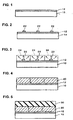
- FIG. 1 - FIG. 8 are views showing a method for manufacturing a ferroelectric capacitor in accordance with a first embodiment of the present invention.
- the first metal film 41 is formed by a sputter method
- the second metal film 46 is formed by a combination of a sputter method and a vapor deposition method.
- the sputter method generally, a film with high adhesion and excellent crystallinity can be obtained.
- the vapor deposition method the energy of particles of an electrode material in a film being grown is low, and the film can be grown in an atmosphere containing few impurities, such that a clean film can be obtained, and internal stress in the formed film is low.
- the intermediate electrode 40 prevention of its exfoliation from the ferroelectric films 30 and 50, excellent crystallinity, and lowered impurity and internal stress can be achieved. Also, in view of the above, excellent ferroelectric characteristics can be obtained in the ferroelectric film 50 that is formed on the intermediate electrode 40.
- interlayer dielectric layers for example, SiO 2 layers
- the cost can be reduced, and the process can be simplified.
- the description is made as to an example in which the lower electrode 20 or the upper electrode 60 is formed in plural divided stages, but the present embodiment is not limited to the above.
- the lower electrode 20 (or the upper electrode 60) may be formed only by a sputter method or a vapor deposition method.
- a plurality of intermediate electrodes 40 and 48 can be formed, as shown in FIG. 9.
- ferroelectric capacitors in three or more layers can be laminated.
- a ferroelectric capacitor 3 has a lower electrode 20, a plurality of intermediate electrodes 40 and 48, and an upper electrode 80 successively disposed, wherein ferroelectric films 30, 50 and 70 are provided between the electrodes, respectively.
- the plurality of intermediate electrodes 40 and 48 may be formed by the same process. Accordingly, as for the respective intermediate electrodes 40 and 48, prevention of their exfoliation from the ferroelectric films 30, 50 and 70, excellent crystallinity, and lowered impurity and internal stress can be achieved.
- the ferroelectric capacitor described above was manufactured, and its ferroelectric characteristics were examined. First, the sample is described.
- a base substrate 10 in which a silicon thermal oxidation film was formed as an interlayer dielectric layer on a surface of a silicon substrate was used. Also, a TiO x film was formed as an adhesion layer 12 by a sputter method on the surface of the base substrate 10.
- a Pt initial crystal nucleus 22 was formed to a thickness of 40 nm or greater by an ion beam sputter method at a base substrate temperature of 800 °C or below. Then, an Ir diffusion prevention film was formed by an ion beam sputter method to a thickness of 10 nm or less at room temperature. Then, a Pt grown layer 24 was formed by a vapor deposition method to a thickness of 100 nm or greater at a base substrate temperature of 200 °C or below. It is noted that the Ir diffusion prevention film was provided to improve the fatigue characteristic of the ferroelectric capacitor, as described above.
- a ferroelectric film 30 was formed on the lower electrode 20. More specifically, first, a series of steps including a mixed solution coating step (by a spin coat method), an alcohol removal step, a dry thermal treatment step, and a cleaning thermal treatment step (at 150 °C in the first time and at 300 °C in the second time) were repeated a desired number of times. Then, sintering was conducted at 650 °C by crystallization annealing to form a ferroelectric film. In the present example, the ferroelectric film having a composition of Pb (Zr 0.17 Ti 0.66 Nb 0.17 ) O 3 was formed.
- a first metal layer 41 composed of Pt was formed by a DC sputter method to a thickness of 40 nm or greater at a base substrate temperature of 800 °C or below. Then, a Pt initial crystal nucleus 42, an Ir diffusion prevention film and a Pt grown layer 44 were formed under conditions similar to those applied to the lower electrode 20.
- a ferroelectric film 50 was formed on the intermediate electrode 40 under conditions similar to those applied to the ferroelectric film 30, and then an upper electrode 60 was formed on the ferroelectric film 50 under conditions similar to those applied to the intermediate electrode 40.
- FIG. 10 is a graph showing hysteresis characteristics of the ferroelectric film between the lower electrode and the intermediate electrode
- FIG. 11 is a graph showing hysteresis characteristics of the ferroelectric film between the intermediate electrode and the upper electrode. It is noted that the characteristics shown in FIG. 10 were measured in a state before the ferroelectric film 50 was formed on the intermediate electrode 40.
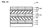
- FIG. 12 - FIG. 14 are views showing a method for manufacturing a ferroelectric capacitor in accordance with a second embodiment of the present invention. It is noted that the present embodiment includes contents that can be derived from the first embodiment.
- the first metal film 141 is formed by a sputter method
- the second metal film 146 is formed by a vapor deposition method.
- the sputter method generally, a film with high adhesion and excellent crystallinity can be obtained.
- the vapor deposition method the energy of particles of an electrode material in a film being grown is low, and the film can be grown in an atmosphere containing few impurities, such that a clean film can be obtained, and internal stress in the formed film is low. Accordingly, as for the intermediate electrode 140, prevention of its exfoliation from the ferroelectric films 130 and 150, excellent crystallinity, and lowered impurity and internal stress can be achieved. Also, in view of the above, excellent ferroelectric characteristics can be obtained in the ferroelectric film 150 that is formed on the intermediate electrode 140.
- FIG. 15 (A) is a plan view of a ferroelectric memory device in accordance with the present embodiment
- FIG. 15 (B) is a cross-sectional view of the ferroelectric memory device in accordance with the present embodiment.
- the ferroelectric memory device 1000 has a ferroelectric memory cell array 200 and a peripheral circuit section 300, as shown in FIG. 15 (A).
- the ferroelectric memory cell array 200 and the peripheral circuit section 300 are formed in different layers, respectively.
- the peripheral circuit section 300 is formed in an area different from the ferroelectric memory cell array 200 on a semiconductor substrate 400.
- a Y-gate, a sense amplifier, an I/O buffer, an X-address decoder, a Y-address decoder, and an address buffer can be enumerated.
- the ferroelectric memory cell array 200 includes lower electrodes 20 (first word lines) for selection of rows, intermediate electrodes 40 (bit lines) for selection of columns, and upper electrodes 60 (second word lines) for selection of rows, which are disposed orthogonal to one another. Also, the lower electrodes 20, the intermediate electrodes 40 and the upper electrodes 60 have stripe configurations formed from signal electrodes in multiple lines.
- a ferroelectric film 30 is provided between the lower electrode 20 and the intermediate electrode 40, and a ferroelectric film 50 is provided between the intermediate electrode 40 and the upper electrode 60.
- a memory cell that functions as the ferroelectric capacitor 1 is formed in an area where the lower electrode 20 and the intermediate electrode 40 intersect each other (or an area where the intermediate electrode 40 and the upper electrode 60 intersect each other). Because this memory cell uses a multilayer type structure of ferroelectric capacitors, a highly integrated and miniaturized ferroelectric memory device can be provided.
- the ferroelectric films 30 and 50 serve well if they are disposed in areas where at least electrodes intersect one another.
- the ferroelectric memory device 1000 has a second interlayer dielectric film 430 that is formed in a manner to cover the ferroelectric capacitor 1. Further, an insulating protection layer 440 is formed over the second interlayer dielectric film 430 in a manner to cover wiring layers 450 and 460.
- the peripheral circuit section 300 includes a variety of circuits for selectively writing or reading information with respect to the ferroelectric memory cell array 200, as indicated in FIG. 15 (A), and may be composed of, for example, a first drive circuit 310 for selectively controlling the lower electrode 20 and the upper electrode 60, a second drive circuit 320 for selectively controlling the intermediate electrode 40, and other signal detection circuits (illustration thereof omitted) such as a sense amplifier and the like.
- the peripheral circuit 300 includes MOS transistors 330 formed on the semiconductor substrate 400, as shown in FIG. 15 (B).
- the MOS transistor 330 has a gate dielectric film 332, a gate electrode 334, and source/drain regions 336.
- the MOS transistors 330 are isolated from one another by element isolation areas 410.
- a first interlayer dielectric film 420 is formed over the semiconductor substrate 400 on which the MOS transistors 330 are formed. Further, the peripheral circuit section 300 and the ferroelectric memory cell array 200 are electrically connected to one another by the wiring layer 450.
- the ferroelectric memory device 1000 includes the ferroelectric capacitor 1 manufactured by the method described above, such that the electrode films can be prevented from peeling off, and excellent ferroelectric characteristics can be obtained. Also, because the ferroelectric capacitor 1 uses a multilayer type structure, higher integration and miniaturization of memories can be achieved.
- the present invention is not limited to the embodiments described above, and many modifications can be made.
- the present invention may include compositions that are substantially the same as the compositions described in the embodiments (for example, a composition with the same function, method and result, or a composition with the same objects and results).
- the present invention includes compositions in which portions not essential in the compositions described in the embodiments are replaced with others.
- the present invention includes compositions that achieve the same functions and effects or achieve the same objects of those of the compositions described in the embodiments.
- the present invention includes compositions that include publicly known technology added to the compositions described in the embodiments.
Landscapes
- Semiconductor Memories (AREA)
- Fixed Capacitors And Capacitor Manufacturing Machines (AREA)
Applications Claiming Priority (1)
| Application Number | Priority Date | Filing Date | Title |
|---|---|---|---|
| JP2004291346A JP2006108291A (ja) | 2004-10-04 | 2004-10-04 | 強誘電体キャパシタ及びその製造方法、並びに強誘電体メモリ装置 |
Publications (2)
| Publication Number | Publication Date |
|---|---|
| EP1643555A2 true EP1643555A2 (de) | 2006-04-05 |
| EP1643555A3 EP1643555A3 (de) | 2007-03-21 |
Family
ID=35474649
Family Applications (1)
| Application Number | Title | Priority Date | Filing Date |
|---|---|---|---|
| EP05021457A Withdrawn EP1643555A3 (de) | 2004-10-04 | 2005-09-30 | Ferroelektrischer Kondensator, dessen Herstellungsverfahren, und ferroelektrische Speicheranordnung |
Country Status (4)
| Country | Link |
|---|---|
| US (1) | US7179705B2 (de) |
| EP (1) | EP1643555A3 (de) |
| JP (1) | JP2006108291A (de) |
| CN (1) | CN100449685C (de) |
Families Citing this family (8)
| Publication number | Priority date | Publication date | Assignee | Title |
|---|---|---|---|---|
| US7737928B2 (en) * | 2003-07-02 | 2010-06-15 | Kent Displays Incorporated | Stacked display with shared electrode addressing |
| SG135079A1 (en) * | 2006-03-02 | 2007-09-28 | Sony Corp | Memory device which comprises a multi-layer capacitor |
| JP5256466B2 (ja) * | 2008-08-28 | 2013-08-07 | 株式会社ユーテック | 成膜装置及び酸化物薄膜成膜用基板の製造方法 |
| KR102307061B1 (ko) | 2014-08-05 | 2021-10-05 | 삼성전자주식회사 | 반도체 소자의 커패시터 제조 방법 |
| CN108292630B (zh) * | 2015-11-25 | 2023-04-25 | 东丽株式会社 | 铁电体存储元件、其制造方法、以及使用其的存储单元及使用其的无线通信装置 |
| US20190035562A1 (en) * | 2017-05-26 | 2019-01-31 | Flash Power Capacitors, Llc | High energy density capacitor system and method |
| TW202145573A (zh) * | 2020-05-29 | 2021-12-01 | 台灣積體電路製造股份有限公司 | 形成於半導體晶粒上的鐵電金屬-鐵電金屬電容器及其製造方法 |
| US20240389486A1 (en) * | 2023-05-15 | 2024-11-21 | Taiwan Semiconductor Manufacturing Company Limited | Capacitor circuit providing self-adjusting capacitance and methods for forming the same |
Citations (1)
| Publication number | Priority date | Publication date | Assignee | Title |
|---|---|---|---|---|
| JP2001230384A (ja) | 2000-02-17 | 2001-08-24 | Seiko Epson Corp | 多層強誘電体記憶装置 |
Family Cites Families (23)
| Publication number | Priority date | Publication date | Assignee | Title |
|---|---|---|---|---|
| US5206788A (en) * | 1991-12-12 | 1993-04-27 | Ramtron Corporation | Series ferroelectric capacitor structure for monolithic integrated circuits and method |
| JPH09331034A (ja) * | 1996-06-07 | 1997-12-22 | Sharp Corp | 酸化物電極膜の形成方法 |
| US5745335A (en) * | 1996-06-27 | 1998-04-28 | Gennum Corporation | Multi-layer film capacitor structures and method |
| JPH1093030A (ja) * | 1996-09-17 | 1998-04-10 | Toshiba Corp | 強誘電体不揮発性メモリ |
| US5807774A (en) * | 1996-12-06 | 1998-09-15 | Sharp Kabushiki Kaisha | Simple method of fabricating ferroelectric capacitors |
| JP3905977B2 (ja) * | 1998-05-22 | 2007-04-18 | 株式会社東芝 | 半導体装置の製造方法 |
| DE19830569C1 (de) * | 1998-07-08 | 1999-11-18 | Siemens Ag | FeRAM-Anordnung |
| JP3976462B2 (ja) * | 2000-01-26 | 2007-09-19 | エルピーダメモリ株式会社 | 半導体装置の製造方法 |
| JP2001229532A (ja) * | 2000-02-10 | 2001-08-24 | Hitachi Maxell Ltd | 薄膜の形成方法、磁気記録媒体の製造方法及び磁気記録装置 |
| CN1170320C (zh) * | 2000-03-13 | 2004-10-06 | 松下电器产业株式会社 | 半导体装置及其制造方法 |
| US6989304B1 (en) * | 2000-08-11 | 2006-01-24 | Renesas Technology Corp. | Method for manufacturing a ruthenium film for a semiconductor device |
| JP2002305288A (ja) * | 2000-08-25 | 2002-10-18 | Nomura Shinzo | キャパシタ電極構造及び半導体記憶装置 |
| JP2002124645A (ja) * | 2000-10-16 | 2002-04-26 | Sharp Corp | 半導体装置およびその製造方法 |
| JP2002217381A (ja) * | 2000-11-20 | 2002-08-02 | Toshiba Corp | 半導体記憶装置及びその製造方法 |
| KR100389032B1 (ko) * | 2000-11-21 | 2003-06-25 | 삼성전자주식회사 | 강유전체 메모리 장치 및 그의 제조 방법 |
| JP2002190578A (ja) * | 2000-12-21 | 2002-07-05 | Toshiba Corp | 半導体装置およびその製造方法 |
| JP3598068B2 (ja) * | 2001-02-06 | 2004-12-08 | 松下電器産業株式会社 | 半導体装置の製造方法 |
| JP2002289796A (ja) * | 2001-03-26 | 2002-10-04 | Nec Corp | 半導体装置の製造方法 |
| JP2002289801A (ja) * | 2001-03-26 | 2002-10-04 | Seiko Epson Corp | 強誘電体メモリ装置および製造方法 |
| JP4167833B2 (ja) * | 2002-01-24 | 2008-10-22 | 株式会社ユーテック | 成膜装置、酸化物薄膜成膜用基板及びその製造方法 |
| JP2004179419A (ja) * | 2002-11-27 | 2004-06-24 | Toshiba Corp | 半導体装置及びその製造方法 |
| JP4586956B2 (ja) * | 2002-12-24 | 2010-11-24 | セイコーエプソン株式会社 | 電極膜の製造方法 |
| CN100352007C (zh) * | 2003-03-24 | 2007-11-28 | 精工爱普生株式会社 | 电极膜及其制造方法和强电介质存储器及半导体装置 |
-
2004
- 2004-10-04 JP JP2004291346A patent/JP2006108291A/ja not_active Withdrawn
-
2005
- 2005-09-22 US US11/233,264 patent/US7179705B2/en not_active Expired - Fee Related
- 2005-09-28 CN CNB2005101071378A patent/CN100449685C/zh not_active Expired - Fee Related
- 2005-09-30 EP EP05021457A patent/EP1643555A3/de not_active Withdrawn
Patent Citations (1)
| Publication number | Priority date | Publication date | Assignee | Title |
|---|---|---|---|---|
| JP2001230384A (ja) | 2000-02-17 | 2001-08-24 | Seiko Epson Corp | 多層強誘電体記憶装置 |
Also Published As
| Publication number | Publication date |
|---|---|
| US7179705B2 (en) | 2007-02-20 |
| EP1643555A3 (de) | 2007-03-21 |
| JP2006108291A (ja) | 2006-04-20 |
| US20060073616A1 (en) | 2006-04-06 |
| CN100449685C (zh) | 2009-01-07 |
| CN1763911A (zh) | 2006-04-26 |
Similar Documents
| Publication | Publication Date | Title |
|---|---|---|
| US6351006B1 (en) | Ferroelectric capacitor with means to prevent deterioration | |
| KR100417743B1 (ko) | 90 나노미터 이하의 두께를 갖는 강유전성 박막을 지닌강유전성 메모리와 그 제조 방법 | |
| US20030052357A1 (en) | Interlayer oxide containing thin films for high dielectric constant application | |
| JP3832617B2 (ja) | 多層状電極の鉛ゲルマネート強誘電体構造およびその堆積方法 | |
| KR100334354B1 (ko) | 강유전체집적회로의 제조방법 | |
| US7425738B2 (en) | Metal thin film and method of manufacturing the same, dielectric capacitor and method of manufacturing the same, and semiconductor device | |
| US7514272B2 (en) | Method of manufacturing ferroelectric memory device | |
| US7179705B2 (en) | Ferroelectric capacitor and its manufacturing method, and ferroelectric memory device | |
| US20080123243A1 (en) | Ferroelectric capacitor | |
| US20150221516A1 (en) | Process-compatible sputtering target for forming ferroelectric memory capacitor plates | |
| JP4421814B2 (ja) | 容量素子の製造方法 | |
| US7163828B2 (en) | Electrode, method of manufacturing the same, ferroelectric memory, and semiconductor device | |
| WO2003100824A2 (en) | Ferroelectric capacitor and method of manufacturing the same | |
| JPH09129827A (ja) | 強誘電体キャパシタ | |
| US20080019075A1 (en) | Dielectric capacitor | |
| US6312567B1 (en) | Method of forming a (200)-oriented platinum layer | |
| KR100459796B1 (ko) | 스토리지 커패시터의 제조방법 및 이 방법으로 제조된스토리지 커패시터를 이용하여 제조된 반도체 구성요소 | |
| JP4586956B2 (ja) | 電極膜の製造方法 | |
| JP3914171B2 (ja) | 半導体装置及びその製造方法 | |
| JP3239852B2 (ja) | 高誘電率キャパシタ及びその製造方法 | |
| JP2002289809A (ja) | 半導体装置およびその製造方法 | |
| KR20010039395A (ko) | Bst 유전막에 구리를 함유한 커패시터 및 그 제조방법 | |
| JP2001028426A (ja) | 半導体装置およびその製造方法 | |
| JPH08236719A (ja) | 白金薄膜、半導体装置及びそれらの製造方法 | |
| JP2010157748A (ja) | 金属膜およびその製造方法、誘電体キャパシタおよびその製造方法ならびに半導体装置 |
Legal Events
| Date | Code | Title | Description |
|---|---|---|---|
| PUAI | Public reference made under article 153(3) epc to a published international application that has entered the european phase |
Free format text: ORIGINAL CODE: 0009012 |
|
| AK | Designated contracting states |
Kind code of ref document: A2 Designated state(s): AT BE BG CH CY CZ DE DK EE ES FI FR GB GR HU IE IS IT LI LT LU LV MC NL PL PT RO SE SI SK TR |
|
| AX | Request for extension of the european patent |
Extension state: AL BA HR MK YU |
|
| PUAL | Search report despatched |
Free format text: ORIGINAL CODE: 0009013 |
|
| AK | Designated contracting states |
Kind code of ref document: A3 Designated state(s): AT BE BG CH CY CZ DE DK EE ES FI FR GB GR HU IE IS IT LI LT LU LV MC NL PL PT RO SE SI SK TR |
|
| AX | Request for extension of the european patent |
Extension state: AL BA HR MK YU |
|
| AKX | Designation fees paid | ||
| STAA | Information on the status of an ep patent application or granted ep patent |
Free format text: STATUS: THE APPLICATION IS DEEMED TO BE WITHDRAWN |
|
| 18D | Application deemed to be withdrawn |
Effective date: 20070924 |
|
| REG | Reference to a national code |
Ref country code: DE Ref legal event code: 8566 |