EP1644995B1 - Halbleiterbauelement und verfahren zu dessen herstellung - Google Patents
Halbleiterbauelement und verfahren zu dessen herstellung Download PDFInfo
- Publication number
- EP1644995B1 EP1644995B1 EP04762375A EP04762375A EP1644995B1 EP 1644995 B1 EP1644995 B1 EP 1644995B1 EP 04762375 A EP04762375 A EP 04762375A EP 04762375 A EP04762375 A EP 04762375A EP 1644995 B1 EP1644995 B1 EP 1644995B1
- Authority
- EP
- European Patent Office
- Prior art keywords
- group
- layer
- compound
- semiconductor component
- component according
- Prior art date
- Legal status (The legal status is an assumption and is not a legal conclusion. Google has not performed a legal analysis and makes no representation as to the accuracy of the status listed.)
- Expired - Lifetime
Links
- 239000004065 semiconductor Substances 0.000 title claims abstract description 41
- 238000004519 manufacturing process Methods 0.000 title claims abstract description 8
- 238000000034 method Methods 0.000 title claims description 7
- 150000001875 compounds Chemical class 0.000 claims abstract description 43
- 239000000758 substrate Substances 0.000 claims abstract description 20
- 230000005669 field effect Effects 0.000 claims abstract description 8
- 230000009881 electrostatic interaction Effects 0.000 claims abstract description 4
- IJGRMHOSHXDMSA-UHFFFAOYSA-N Atomic nitrogen Chemical compound N#N IJGRMHOSHXDMSA-UHFFFAOYSA-N 0.000 claims description 4
- 125000003277 amino group Chemical group 0.000 claims description 4
- 238000002161 passivation Methods 0.000 claims description 3
- VEXZGXHMUGYJMC-UHFFFAOYSA-M Chloride anion Chemical compound [Cl-] VEXZGXHMUGYJMC-UHFFFAOYSA-M 0.000 claims description 2
- OAICVXFJPJFONN-UHFFFAOYSA-N Phosphorus Chemical compound [P] OAICVXFJPJFONN-UHFFFAOYSA-N 0.000 claims description 2
- NINIDFKCEFEMDL-UHFFFAOYSA-N Sulfur Chemical compound [S] NINIDFKCEFEMDL-UHFFFAOYSA-N 0.000 claims description 2
- 125000003368 amide group Chemical group 0.000 claims description 2
- QVGXLLKOCUKJST-UHFFFAOYSA-N atomic oxygen Chemical compound [O] QVGXLLKOCUKJST-UHFFFAOYSA-N 0.000 claims description 2
- 229920001400 block copolymer Polymers 0.000 claims description 2
- 150000001732 carboxylic acid derivatives Chemical class 0.000 claims description 2
- 125000004093 cyano group Chemical group *C#N 0.000 claims description 2
- 125000000449 nitro group Chemical group [O-][N+](*)=O 0.000 claims description 2
- 229910052757 nitrogen Inorganic materials 0.000 claims description 2
- 150000002905 orthoesters Chemical class 0.000 claims description 2
- 229910052760 oxygen Inorganic materials 0.000 claims description 2
- 239000001301 oxygen Substances 0.000 claims description 2
- 238000012856 packing Methods 0.000 claims description 2
- 229910052698 phosphorus Inorganic materials 0.000 claims description 2
- 239000011574 phosphorus Substances 0.000 claims description 2
- 235000013855 polyvinylpyrrolidone Nutrition 0.000 claims description 2
- 229920000036 polyvinylpyrrolidone Polymers 0.000 claims description 2
- 239000001267 polyvinylpyrrolidone Substances 0.000 claims description 2
- 229910052717 sulfur Inorganic materials 0.000 claims description 2
- 239000011593 sulfur Substances 0.000 claims description 2
- 229920006301 statistical copolymer Polymers 0.000 claims 1
- 239000012808 vapor phase Substances 0.000 claims 1
- 239000010410 layer Substances 0.000 description 49
- 239000002356 single layer Substances 0.000 description 5
- 238000000151 deposition Methods 0.000 description 4
- 239000007789 gas Substances 0.000 description 4
- SLIUAWYAILUBJU-UHFFFAOYSA-N pentacene Chemical compound C1=CC=CC2=CC3=CC4=CC5=CC=CC=C5C=C4C=C3C=C21 SLIUAWYAILUBJU-UHFFFAOYSA-N 0.000 description 4
- 229910004298 SiO 2 Inorganic materials 0.000 description 3
- 239000002800 charge carrier Substances 0.000 description 3
- 230000008021 deposition Effects 0.000 description 3
- 230000000694 effects Effects 0.000 description 3
- 230000006870 function Effects 0.000 description 3
- 230000008569 process Effects 0.000 description 3
- 239000000126 substance Substances 0.000 description 3
- 230000008901 benefit Effects 0.000 description 2
- 238000012937 correction Methods 0.000 description 2
- 239000003574 free electron Substances 0.000 description 2
- 239000000463 material Substances 0.000 description 2
- 239000002904 solvent Substances 0.000 description 2
- 229910018557 Si O Inorganic materials 0.000 description 1
- BLRPTPMANUNPDV-UHFFFAOYSA-N Silane Chemical group [SiH4] BLRPTPMANUNPDV-UHFFFAOYSA-N 0.000 description 1
- XUIMIQQOPSSXEZ-UHFFFAOYSA-N Silicon Chemical compound [Si] XUIMIQQOPSSXEZ-UHFFFAOYSA-N 0.000 description 1
- XBDYBAVJXHJMNQ-UHFFFAOYSA-N Tetrahydroanthracene Natural products C1=CC=C2C=C(CCCC3)C3=CC2=C1 XBDYBAVJXHJMNQ-UHFFFAOYSA-N 0.000 description 1
- WLPWBUSZWTZYTQ-UHFFFAOYSA-N amino(aminoazo)amine Chemical compound NNN=NN WLPWBUSZWTZYTQ-UHFFFAOYSA-N 0.000 description 1
- 238000013459 approach Methods 0.000 description 1
- 230000015572 biosynthetic process Effects 0.000 description 1
- 239000011248 coating agent Substances 0.000 description 1
- 238000000576 coating method Methods 0.000 description 1
- 238000010276 construction Methods 0.000 description 1
- 238000013461 design Methods 0.000 description 1
- 239000010432 diamond Substances 0.000 description 1
- 239000003989 dielectric material Substances 0.000 description 1
- 238000009792 diffusion process Methods 0.000 description 1
- 238000005516 engineering process Methods 0.000 description 1
- PCHJSUWPFVWCPO-UHFFFAOYSA-N gold Chemical compound [Au] PCHJSUWPFVWCPO-UHFFFAOYSA-N 0.000 description 1
- 239000010931 gold Substances 0.000 description 1
- 229910052737 gold Inorganic materials 0.000 description 1
- 238000007654 immersion Methods 0.000 description 1
- 239000011159 matrix material Substances 0.000 description 1
- 238000005259 measurement Methods 0.000 description 1
- 238000012986 modification Methods 0.000 description 1
- 230000004048 modification Effects 0.000 description 1
- 229920000123 polythiophene Polymers 0.000 description 1
- 229920005604 random copolymer Polymers 0.000 description 1
- 229910052710 silicon Inorganic materials 0.000 description 1
- 239000010703 silicon Substances 0.000 description 1
- LIVNPJMFVYWSIS-UHFFFAOYSA-N silicon monoxide Inorganic materials [Si-]#[O+] LIVNPJMFVYWSIS-UHFFFAOYSA-N 0.000 description 1
- 230000009897 systematic effect Effects 0.000 description 1
- IFLREYGFSNHWGE-UHFFFAOYSA-N tetracene Chemical compound C1=CC=CC2=CC3=CC4=CC=CC=C4C=C3C=C21 IFLREYGFSNHWGE-UHFFFAOYSA-N 0.000 description 1
- PYJJCSYBSYXGQQ-UHFFFAOYSA-N trichloro(octadecyl)silane Chemical class CCCCCCCCCCCCCCCCCC[Si](Cl)(Cl)Cl PYJJCSYBSYXGQQ-UHFFFAOYSA-N 0.000 description 1
- 238000007740 vapor deposition Methods 0.000 description 1
Images


Classifications
-
- H—ELECTRICITY
- H10—SEMICONDUCTOR DEVICES; ELECTRIC SOLID-STATE DEVICES NOT OTHERWISE PROVIDED FOR
- H10K—ORGANIC ELECTRIC SOLID-STATE DEVICES
- H10K10/00—Organic devices specially adapted for rectifying, amplifying, oscillating or switching; Organic capacitors or resistors having potential barriers
- H10K10/40—Organic transistors
- H10K10/46—Field-effect transistors, e.g. organic thin-film transistors [OTFT]
- H10K10/462—Insulated gate field-effect transistors [IGFETs]
- H10K10/466—Lateral bottom-gate IGFETs comprising only a single gate
-
- C—CHEMISTRY; METALLURGY
- C23—COATING METALLIC MATERIAL; COATING MATERIAL WITH METALLIC MATERIAL; CHEMICAL SURFACE TREATMENT; DIFFUSION TREATMENT OF METALLIC MATERIAL; COATING BY VACUUM EVAPORATION, BY SPUTTERING, BY ION IMPLANTATION OR BY CHEMICAL VAPOUR DEPOSITION, IN GENERAL; INHIBITING CORROSION OF METALLIC MATERIAL OR INCRUSTATION IN GENERAL
- C23C—COATING METALLIC MATERIAL; COATING MATERIAL WITH METALLIC MATERIAL; SURFACE TREATMENT OF METALLIC MATERIAL BY DIFFUSION INTO THE SURFACE, BY CHEMICAL CONVERSION OR SUBSTITUTION; COATING BY VACUUM EVAPORATION, BY SPUTTERING, BY ION IMPLANTATION OR BY CHEMICAL VAPOUR DEPOSITION, IN GENERAL
- C23C18/00—Chemical coating by decomposition of either liquid compounds or solutions of the coating forming compounds, without leaving reaction products of surface material in the coating; Contact plating
- C23C18/16—Chemical coating by decomposition of either liquid compounds or solutions of the coating forming compounds, without leaving reaction products of surface material in the coating; Contact plating by reduction or substitution, e.g. electroless plating
- C23C18/18—Pretreatment of the material to be coated
- C23C18/1851—Pretreatment of the material to be coated of surfaces of non-metallic or semiconducting in organic material
-
- C—CHEMISTRY; METALLURGY
- C23—COATING METALLIC MATERIAL; COATING MATERIAL WITH METALLIC MATERIAL; CHEMICAL SURFACE TREATMENT; DIFFUSION TREATMENT OF METALLIC MATERIAL; COATING BY VACUUM EVAPORATION, BY SPUTTERING, BY ION IMPLANTATION OR BY CHEMICAL VAPOUR DEPOSITION, IN GENERAL; INHIBITING CORROSION OF METALLIC MATERIAL OR INCRUSTATION IN GENERAL
- C23C—COATING METALLIC MATERIAL; COATING MATERIAL WITH METALLIC MATERIAL; SURFACE TREATMENT OF METALLIC MATERIAL BY DIFFUSION INTO THE SURFACE, BY CHEMICAL CONVERSION OR SUBSTITUTION; COATING BY VACUUM EVAPORATION, BY SPUTTERING, BY ION IMPLANTATION OR BY CHEMICAL VAPOUR DEPOSITION, IN GENERAL
- C23C18/00—Chemical coating by decomposition of either liquid compounds or solutions of the coating forming compounds, without leaving reaction products of surface material in the coating; Contact plating
- C23C18/16—Chemical coating by decomposition of either liquid compounds or solutions of the coating forming compounds, without leaving reaction products of surface material in the coating; Contact plating by reduction or substitution, e.g. electroless plating
- C23C18/18—Pretreatment of the material to be coated
- C23C18/1851—Pretreatment of the material to be coated of surfaces of non-metallic or semiconducting in organic material
- C23C18/1855—Pretreatment of the material to be coated of surfaces of non-metallic or semiconducting in organic material by mechanical pretreatment, e.g. grinding, sanding
- C23C18/1858—Pretreatment of the material to be coated of surfaces of non-metallic or semiconducting in organic material by mechanical pretreatment, e.g. grinding, sanding by formation of electrostatic charges, e.g. tribofriction
-
- H—ELECTRICITY
- H10—SEMICONDUCTOR DEVICES; ELECTRIC SOLID-STATE DEVICES NOT OTHERWISE PROVIDED FOR
- H10K—ORGANIC ELECTRIC SOLID-STATE DEVICES
- H10K71/00—Manufacture or treatment specially adapted for the organic devices covered by this subclass
- H10K71/10—Deposition of organic active material
- H10K71/191—Deposition of organic active material characterised by provisions for the orientation or alignment of the layer to be deposited
-
- H—ELECTRICITY
- H10—SEMICONDUCTOR DEVICES; ELECTRIC SOLID-STATE DEVICES NOT OTHERWISE PROVIDED FOR
- H10K—ORGANIC ELECTRIC SOLID-STATE DEVICES
- H10K85/00—Organic materials used in the body or electrodes of devices covered by this subclass
- H10K85/60—Organic compounds having low molecular weight
- H10K85/615—Polycyclic condensed aromatic hydrocarbons, e.g. anthracene
-
- H—ELECTRICITY
- H10—SEMICONDUCTOR DEVICES; ELECTRIC SOLID-STATE DEVICES NOT OTHERWISE PROVIDED FOR
- H10K—ORGANIC ELECTRIC SOLID-STATE DEVICES
- H10K85/00—Organic materials used in the body or electrodes of devices covered by this subclass
- H10K85/701—Langmuir Blodgett films
Definitions
- the invention relates to a semiconductor component according to the preamble of claim 1 and to a method for producing a layer on a substrate according to the preamble of claim 12.
- Organic semiconductor layer-based organic field effect transistors are of interest for a variety of electronic applications requiring low manufacturing costs, flexible or unbreakable substrates, or the fabrication of transistors and integrated circuits over large active areas.
- organic field effect transistors are useful as pixel controls in active matrix displays or for the fabrication of extremely low cost integrated circuits, such as those used for active identification and identification of goods and goods, but also for future organic control circuits memory elements.
- a third possibility is the dynamic operation of a circuit.
- a circuit system is activated by applying an external pulse voltage ( W. Fix, A. Ullmann, J. Ficker, W. Clemens Applied Physics Letters, 2002, 81, 1735-1737 ).
- W. Fix A. Ullmann, J. Ficker, W. Clemens Applied Physics Letters, 2002, 81, 1735-1737 .
- This is possible in principle for simple demonstrator circuits, but very complex for more complex logic circuits.
- the object of this invention is to modify the OFETs in such a way that the additional correction of the levelshift becomes superfluous.
- the semiconductor component according to the invention has a layer with a compound which has at least one anchor group for producing a bond with a substrate and at least one group having at least one free electron pair and / or one dipole moment.
- the anchor group is necessary for a stationary layer to form.
- the effect of the invention is based on the fact that the introduced compound closes on a charge traps (traps) and at the same time by their high order the molecular properties of the molecules (dipole moment) forms a macroscopic effect, the electrochemical and electrical properties of a e.g. Overlying organic semiconductor layer and the morphology favorably influenced.
- At least one anchor group is covalently bondable to a dielectric layer. It is particularly advantageous if at least one anchor group is a silicon-halogen group, a silicon-alkoxy group, an amino group, an amide group or a reactive carboxylic acid derivative, in particular a chloride or an orthoester.
- the group for generating a Dipolmomente s a polar group, in particular an amino group, a cyano group, a nitro group or a ferrocenyl group. Furthermore, it is advantageous if the group having a free electron pair oxygen, nitrogen, sulfur and / or phosphorus.
- the compound has the ability to form monomolecular layers on the substrate, particularly a dielectric layer, semiconductor devices can be easily built up from layers.
- monolayers are particularly facilitated when the compound is substantially linear or has a long axis compared to other groups of the compound. Also, it is particularly advantageous for monolayers when the anchor group and the group with the dipole moment or the group with a lone pair of electrons are arranged at opposite ends of the linear compound. It is particularly advantageous if a part of the compound has an increased affinity for the surface of the substrate, in particular a dielectric layer, and that at the opposite end of the compound a high packing density group is arranged which is inert to the substrate.
- the compound is a polyvinylpyrrolidone, a pyridilinone or random or block copolymers containing these units.
- the object is also achieved by a method for producing the semiconductor component with the features of claim 12.
- a substrate in particular a component substrate with a dielectric layer, immersed in a solution or deposited from a gas phase, wherein the solution or the gas phase contains at least one of the compounds according to claim 1 to 11.
- the chemical compound should in this case as thin as possible, preferably as a monolayer, and be applied inexpensively. It should be as chemically fixed in the channel (covalently bonded to the dielectric) to diffusion processes avoid. Due to the nature of the chemical compound, the value for the threshold voltage should be able to be adjusted in order to obtain an optimum / adjustable value of the threshold voltage in the respective application.
- the concentration of the compound in the solution is between 0.1 and 1%.
- a semiconductor component in particular an OFET, can be produced if, after the application of the layer with the compound according to at least one of claims 1 to 11, a source-drain layer and an organic semiconductor layer are applied.
- Fig. 1 shows a schematic sectional view through an organic field effect transistor (OFET).
- OFET organic field effect transistor
- Organic field-effect transistors are electronic components consisting of multiple layers (layers), all of which are structured to generate integrated circuits through interconnections of individual layers. It shows Fig. 1 the basic structure of such a transistor in a bottom-contact architecture.
- a gate electrode 21 is arranged, which is covered by a gate dielectric layer 22.
- Such dielectrics have a layer thickness of less than 5 nm (bottom up).
- a layer for adjusting the threshold voltage 10 is arranged in a region; the gate dielectric layer 22 thus forms the substrate for the threshold voltage adjustment layer 10.
- This threshold voltage adjustment layer 10 is connected at the top to an active semiconducting layer 24 (here pentacene). Laterally, a source layer 23a and a drain layer 23b are arranged, both of which also communicate with the overlying active semiconducting layer 24. Over the active layer 24, a passivation layer 25 is arranged.
- Fig. 2 is the area of the charge carrier channel in the OFET according to Fig. 1 shown enlarged.
- the diamonds 11 are intended to control the electrostatic interactions between the layer Setting the threshold voltage 10 and the overlying active layer 25 symbolize.
- Fig. 3a to 3c three embodiments of the compounds of the invention are shown. All three compounds KBM, APTS and APPTS have an anchor group 1, which is formed as a silane group. With this anchor group 1, the compound can bond to a substrate such as the dielectric layer 22 in FIG Fig. 2 received. Due to the substantially linear nature of the three compounds, monolayers can form in which the longitudinal axes of the connection are aligned parallel to each other and perpendicular to the dielectric layer 22. All three compounds also have polar groups 2 at the ends of the compound opposite to the anchor group 1.
- a monolayer 10 of any of these compounds according to Fig. 2 acts in such a way that it electrically interacts with an overlying semiconductor layer 24 (eg pentacene) and thereby alters the semiconductive properties so that the threshold voltage can be influenced in a targeted manner, in particular that it is lowered.
- an overlying semiconductor layer 24 eg pentacene
- the process for this can be a simple immersion process, in which the substrate is immersed in a dilute solution (solvent with about 0.1 -1% substance).
- a dilute solution solvent with about 0.1 -1% substance.
- the molecules bind to the dielectric layer 22 by means of their anchor group 1. or alkoxysilane selectively to an OH-functionalized surface to form a Si-O bond. The excess material is then washed off with pure solvent.
- a gas phase deposition is possible.
- the compounds shown are each applied as a monolayer from the gas phase on highly doped thermally oxidized (100 nm SiO 2 ) silicon wafer. Subsequently, a 30 nm thick layer 24 pentazene (organic semiconductor) is evaporated.
- source and drain contacts 23a, 23b are defined by vapor deposition of a 30 nm thick gold layer (structuring takes place by applying a shadow mask). Subsequently, the transistors are electrically characterized.
- an OFET is prepared and measured as a reference in the same manner without such a monolayer.
- a coating with OTS was also used for comparison purposes.
- the results of the measured threshold voltages are shown in Tables 1 and Fig. 4a shown.
- the correlation of the measured threshold voltages with the dipole moment of the respective compound is in Fig. 4b shown. This clearly shows that the threshold voltage can be selectively adjusted depending on the connections.
- the threshold voltages correlate with molecular properties (such as dipole moment) and layer properties (such as surface free energy). It can be clearly seen that the threshold voltage is significantly reduced compared to the reference (no separate layer) and also to OTS.
- the main advantage of this invention is that such a simple process described here of chemically modifying the dielectric surface and thus the Charge carrier channel, the previously necessary solution of the problem of positive threshold voltages in OFETs by Levelshift completely redundant and thus saves about 50 percent of the required transistors per circuit.
- Table 1 SAM material Vth [V] no SAM (reference) 2 OTS -1 APPTS -17 APTS -35 KBM -43
Landscapes
- Chemical & Material Sciences (AREA)
- Engineering & Computer Science (AREA)
- Metallurgy (AREA)
- Chemical Kinetics & Catalysis (AREA)
- Materials Engineering (AREA)
- Mechanical Engineering (AREA)
- General Chemical & Material Sciences (AREA)
- Organic Chemistry (AREA)
- Manufacturing & Machinery (AREA)
- Thin Film Transistor (AREA)
- Electrodes Of Semiconductors (AREA)
- Heterocyclic Carbon Compounds Containing A Hetero Ring Having Oxygen Or Sulfur (AREA)
- Junction Field-Effect Transistors (AREA)
Abstract
Description
- Die Erfindung betrifft ein Halbleiterbauelement nach dem Oberbegriff des Anspruchs 1 und ein Verfahren zur Herstellung einer Schicht auf einem Substrat nach dem Oberbegriff des Anspruchs 12.
- Organische Feldeffekttransistoren (OFETs) auf der Basis organischer Halbleiterschichten sind von Interesse für eine Vielzahl elektronischer Anwendungen, die niedrige Fertigungskosten, flexible oder unzerbrechliche Substrate, oder die Herstellung von Transistoren und integrierten Schaltungen über große aktive Flächen erfordern. Zum Beispiel eignen sich organische Feldeffekttransistoren als Pixel-Steuerelemente in Aktiv- Matrix-Bildschirmen oder für die Herstellung von extrem preiswerten integrierten Schaltungen, wie sie zum Beispiel für die aktive Kennzeichnung und Identifizierung von Waren und Gütern zum Einsatz kommen, aber auch für zukünftige Steuerschaltungen organischer Speicherelemente.
- Transistoren und integrierte Schaltungen (ICs) basierend auf organischen Halbleiterschichten arbeiten heute weitestgehend auf p-MOS Technologie, da im Wesentlichen nur organische p-Halbleiter stabil genug sind um langlebige Devices herzustellen.
- Die meisten bisher bekannten organischen Halbleiter (z.B. Pentazen, Tetrazen, Oligo- und Polythiophene), die auch von ihrer Ladungsträgerbeweglichkeit für Anwendungen in Betracht kommen, weisen in Transistoren meist eine leicht positive Schwellspannung auf d.h. die Transistoren schalten bei einem Potential von 0 V an der Gateelektrode noch nicht vollständig aus. Dies hat zur Konsequenz, dass einfache Inverter (zwei Transistoren) nicht die korrekte logische Funktion zeigen und darauf basierte Ringoszillatoren nicht oszillieren.
- Bisher wird dieses Problem schaltungstechnisch in der Weise gelöst, dass Inverter und daraus resultierende Schaltungen mit einem integrierten "Levelshift" hergestellt werden. Diese zusätzliche "Korrektur" der logischen Funktion hat zur Konsequenz, dass sich die Anzahl der Transistoren für einen funktionsfähigen Inverter von zwei auf vier verdoppelt (H. Klauk, D.J. Gundlach, T.N. Jackson IEEE Electron Device Letters, 1999, 20, 289-291).
- Zudem wird eine weitere Versorgungsspannung für den Levelshifter benötigt.
- Des Weiteren existieren Ansätze durch die Wahl eines geeigneten Gatedielektrikums (anorganisch oder organisch) die Schwellspannung einzustellen (siehe H. Klauk, M. Halik, U. Zschieschang, G. Schmid, W. Radlik, W. Weber Journal of Applied Physics, 2002, 92, 5259-5263). Dabei zeigte sich jedoch, dass Werte im negativen Bereich (ca. -8V) erreicht wurden, die Schwankungen dieser Werte jedoch relativ groß sind (+/- 10V) und damit derzeit kein zuverlässiges Schaltungsdesign für ICs möglich ist. Auch ist zwar beschrieben dass eine Monolage von Octadecyltrichlorosilane (OTS) im Fall von SiO2 als Gatedielektrikum in Pentazentransistoren eine Verschiebung der Schwellspannung verglichen mit blanken SiO2 als Gatedielektrikum um wenige Volt bewirkt, jedoch nicht in der Weise, dass eine systematische und vor allem definierte Einstellung der Schwellspannung vorgenommen werden kann.
- Eine dritte Möglichkeit besteht im dynamischen Betrieb einer Schaltung. Dabei wird ein Schaltungssystem durch Anlegen einer externen Impulsspannung aktiviert (W. Fix, A. Ullmann, J. Ficker, W. Clemens Applied Physics Letters, 2002, 81, 1735-1737). Dies ist für einfache Demonstratorschaltungen prinzipiell möglich, jedoch für komplexere logische Schaltungen sehr aufwändig.
- Aufgabe dieser Erfindung ist es, die OFETs in der Weise zu modifizieren, so dass die zusätzliche Korrektur der logischen Funktion (levelshift) überflüssig wird.
- Diese Aufgabe wird erfindungsgemäß durch ein Halbleiterbauelement mit den Merkmalen des Anspruchs 1 gelöst.
- Das erfindungsgemäße Halbleiterbauelement weist eine Schicht mit einer Verbindung auf, die mindestens eine Ankergruppe zur Herstellung einer Bindung mit einem Substrat und mindestens eine Gruppe mit mindestens einem freien Elektronenpaar und / oder einem Dipolmoment aufweist. Die Ankergruppe ist notwendig, damit sich eine ortsfeste Schicht ausbilden kann.
- Der erfindungsgemäße Effekt beruht darauf, dass die eingebrachte Verbindung zum einen Ladungsträgersenken (Traps) schließt und gleichzeitig durch deren hohe Ordnung die molekularen Eigenschaften der Moleküle (Dipolmoment) einen makroskopische Effekt ausbildet, der die elektrochemischen und elektrischen Eigenschaften einer z.B. darüber liegenden organischen Halbleiterschicht und die Morphologie günstig beeinflusst.
- Dies hat die Wirkung, dass sich die Zahl der Transistoren für eine logische Schaltung nahezu halbieren würde, somit auch weniger Interconnects und Vias benötigt würden und daraus folgend die benötigte Fläche für die Schaltung kleiner würde. Des Weiteren sollte sich die Ausbeute erhöhen. Die zweite Versorgungsspannung für den Levelshifter entfällt ebenfalls. Diese Modifikation erfolgt auf chemischem Wege in der Weise, dass in den Kanal des Transistors (Strecke auf dem Dielektrikum zwischen Source und Drain Elektrode) vor Abscheiden des organischen Halbleiters eine chemische Verbindung ein-/aufgebracht wird, welche die elektrischen Eigenschaften des organischen Halbleiters bei Anlegen einer Spannung beeinflusst.
- In einer vorteilhaften Ausgestaltung ist mindestens eine Ankergruppe kovalent an eine dielektrische Schicht bindbar. Besonders vorteilhaft ist es, wenn mindestens eine Ankergruppe eine Silizium-Halogen-Gruppe, eine Silizium-Alkoxy-Gruppe, eine Aminogruppe, eine Amidgruppe oder ein reaktives Carbonsäurederivat, insbesondere ein Chlorid oder ein Orthoester ist.
- In einer weiteren vorteilhaften Ausgestaltung weist die Gruppe zur Erzeugung eines Dipolmomentes eine polare Gruppe, insbesondere eine Aminogruppe, eine Cyanogruppe, eine Nitrogruppe oder eine Ferrocenylgruppe auf. Ferner ist es vorteilhaft, wenn die Gruppe mit einem freien Elektronenpaar Sauerstoff, Stickstoff, Schwefel und / oder Phosphor aufweist.
- Wenn die Verbindung die Fähigkeit zur Bildung monomolekularer Schichten auf dem Substrat, insbesondere einer dielektrischen Schicht aufweist, lassen sich Halbleiterbauelemente in einfacher Weise aus Schichten aufbauen.
- Die Bildung von Monolagen wir insbesondere erleichtert, wenn die Verbindung im Wesentlichen linear ausgebildet ist oder eine im Vergleich zu anderen Gruppen der Verbindung lange Achse aufweist. Auch ist es insbesondere für Monolagen vorteilhaft, wenn die Ankergruppe und die Gruppe mit dem Dipolmoment oder die Gruppe mit einem freien Elektronenpaar an gegenüber liegenden Enden der linearen Verbindung angeordnet sind. Besonders vorteilhaft ist es, wenn ein Teil der Verbindung eine erhöhte Affinität zur Oberfläche des Substrates, insbesondere einer dielektrischen Schicht, aufweist, und dass am entgegengesetzten Ende der Verbindung eine Gruppe mit hoher Packungsdichte angeordnet ist, die inert zum Substrat ist.
- Besonders gezielt lässt sich die Schwellspannung unterdrücken, wenn die Verbindung eine der folgenden Strukturen aufweist:

- Auch ist es vorteilhaft, wenn die Verbindung ein Polyvinylpyrrolidon, ein Pyridilinon oder statistische oder Block-Kopolymere, die diese Einheiten enthalten, ist.
- Die Aufgabe wird auch durch ein Verfahren zur Herstellung des Halbleiterbauelementes mit dem Merkmalen des Anspruchs 12 gelöst.
- Dabei wird ein Substrat, insbesondere ein Bauelementsubstrat mit einer dielektrischen Schicht, in eine Lösung getaucht oder aus einer Gasphase abgeschieden, wobei die Lösung oder die Gasphase mindestens eine der Verbindungen gemäß Anspruch 1 bis 11 enthält.
- Die chemische Verbindung soll hierbei möglichst dünn, bevorzugt als Monolage, und preiswert aufgebracht werden. Sie soll im Kanal möglichst chemisch fixiert sein (kovalent gebunden an das Dielektrikum) um Diffusionsprozesse zu vermeiden. Durch die Art der chemischen Verbindung sollte sich der Wert für die Schwellspannung justieren lassen, um ein optimalen/einstellbaren Wert der Schwellspannung bei der jeweiligen Anwendung zu erhalten.
- Für den Fall der Abscheidung aus der Lösung ist es vorteilhaft, wenn Konzentration der Verbindung in der Lösung zwischen 0,1 und 1% beträgt.
- Vorteilhafterweise lässt sich ein Halbleiterbauelement, insbesondere ein OFET, herstellen, wenn nach dem Aufbringen der Schicht mit der Verbindung nach mindestens einem der Ansprüche 1 bis 11 eine Source-Drain Schicht und eine organische Halbleiterschicht aufgebracht wird.
- Die Erfindung wird nachfolgend unter Bezugnahme auf die Figuren der Zeichnungen an mehreren Ausführungsbeispielen näher erläutert. Es zeigen:
- Fig. 1
- eine schematische Schnittansicht durch einen organischen Feldeffekttransistor;
- Fig. 2
- eine schematische Darstellung einer Schichtenstruktur mit einer Schicht mit einer erfindungsgemäßen Verbindung;
- Fig. 3a-c
- Strukturformeln von Ausführungsformen der erfindungsgemäßen Verbindung;
- Fig. 4a
- Messergebnis der Schwellspannung in Abhängigkeit der ausgewählten Verbindung;
- Fig. 4b
- Korrelation der gemessenen Schwellspannung mit dem Dipolmoment;
- Tab. 1
- Schwellspannung bei OFET mit unterschiedlichen Substanzen.
- Bevor auf Ausführungsbeispiele für die erfindungsgemäßen Halbleiterbauelemente eingegangen wird, soll anhand der
Fig. 1 und2 der Aufbau eines organischen Feldeffekttransistors als Halbleiterbauelement erläutert werden. -
Fig. 1 zeigt dabei eine schematische Schnittansicht durch einen organischen Feldeffekttransistor (OFET). - Organische Feldeffekttransistoren sind elektronische Bauteile, die aus mehreren Schichten (Lagen) bestehen, welche alle strukturiert sind, um durch Verbindungen einzelner Schichten integrierte Schaltungen zu generieren. Dabei zeigt
Fig. 1 den prinzipiellen Aufbau eines solchen Transistors in einer Bottom-Kontakt Architektur. - Auf einem Basis-Substrat 20 ist eine Gateelektrode 21 angeordnet, die von einer Gatedielektrikumsschicht 22 überdeckt ist. Derartige Dielektrika besitzen eine Schichtdicke von weniger als 5 nm (Bottom up).
- Auf der Gatedielektrikumsschicht 22 ist in einem Bereich eine Schicht zur Einstellung der Schwellspannung 10 angeordnet; die Gatedielektrikumsschicht 22 bildet damit das Substrat für die Schicht zur Einstellung der Schwellspannung 10. Diese Schicht zur Einstellung der Schwellspannung 10 steht nach oben hin mit einer aktiven halbleitenden Schicht 24 (hier mit Pentazen) in Verbindung. Seitlich sind eine Sourceschicht 23a und eine Drainschicht 23b angeordnet, die beide ebenfalls mit der darbüberliegenden aktiven halbleitenden Schicht 24 in Verbindung stehen. Über der aktiven Schicht 24 ist eine Passivierungsschicht 25 angeordnet.
- In
Fig. 2 ist der Bereich des Ladungsträgerkanals im OFET gemäßFig. 1 vergrößert dargestellt. Die Rauten 11 sollen die elektrostatischen Wechselwirkungen zwischen der Schicht zur Einstellung der Schwellspannung 10 und der darüber liegenden aktiven Schicht 25 symbolisieren. - In den
Fig. 3a bis 3c sind drei Ausführungsformen der erfindungsgemäßen Verbindungen dargestellt. Alle drei Verbindungen KBM, APTS und APPTS weisen eine Ankergruppe 1 auf, die als eine Silangruppe ausgebildet ist. Mit dieser Ankergruppe 1 kann die Verbindung eine Bindung mit einem Substrat, wie z.B. der Dielektrikumsschicht 22 inFig. 2 eingehen. Aufgrund des im Wesentlichen linearen Charakters der drei Verbindungen können sich Monolagen ausbilden, bei denen die Längsachsen der Verbindung jeweils parallel zueinander und senkrecht zur Dielektrikumsschicht 22 ausgerichtet sind. Alle drei Verbindungen weisen darüber hinaus polare Gruppen 2 an den Enden der Verbindung auf, die der Ankergruppe 1 entgegengesetzt ist. - Eine Monolage 10 aus einer dieser Verbindungen gemäß
Fig. 2 wirkt in der Weise, dass sie in elektrischer Wechselwirkung mit einer darüber liegenden Halbleiterschicht 24 (z.B. Pentazen) tritt und dabei die halbleitenden Eigenschaften so ändert, dass die Schwellspannung gezielt beeinflussbar ist, insbesondere dass sie gesenkt wird. - Dies wird in Zusammenhang mit den
Fig. 4a und 4 und Tab. 1 noch erläutert werden. - Der Vorteil einer solchen Schicht 10 mit erfindungsgemäßen Verbindungen (z.B. gemäß
Fig. 3 ) ist, dass sie sich preiswert auf die Transistorstruktur (vor Abscheidung der organischen Halbleiterschicht) aufbringen lässt. - Das Verfahren hierfür kann ein einfacher Tauchprozess sein, bei dem das Substrat in eine verdünnte Lösung (Lösungsmittel mit ca. 0.1 -1 % Substanz) getaucht wird. Hierbei binden sich die Moleküle mittels ihrer Ankergruppe 1 an die dielektrische Schicht 22. Beispielsweise bindet ein Chloro- oder Alkoxysilan selektiv an eine mit OH-Gruppen funktionialisierte Oberfläche unter Ausbildung einer Si-O-Bindung. Das überschüssige Material wird dann mit reinem Lösungsmittel abgewaschen.
- Alternativ ist auch eine Gasphasendeposition möglich. Die in
Fig. 3a bis 3c dargestellten Verbindungen werden dabei jeweils als Monolage aus der Gasphase auf hochdotierte thermisch oxidierte (100 nm SiO2) Siliziumwafer aufgebracht. Anschließend wird eine 30 nm dicke Schicht 24 Pentazen (organischer Halbleiter) aufgedampft. Zur Vervollständigung des Transistoraufbaus werden Source- und Drain-Kontakte (23a, 23b) durch Aufdampfen einer 30 nm dicken Goldschicht (Strukturierung erfolgt durch Auflage einer Schattenmaske) definiert. Im Anschluss werden die Transistoren elektrisch charakterisiert. - Zu Vergleichszwecken werden als Referenz ein OFET in der gleichen Weise ohne eine solche Monolage hergestellt und durchgemessen. Auch eine Beschichtung mit OTS erfolgte zu Vergleichszwecken.
- Die Ergebnisse der gemessenen Schwellspannungen sind in Tabelle 1 und
Fig. 4a dargestellt. Die Korrelation der gemessenen Schwellspannungen mit dem Dipolmoment der jeweiligen Verbindung ist inFig. 4b gezeigt. Dabei zeigt sich deutlich, dass die Schwellspannung in Abhängigkeit von den Verbindungen gezielt einstellbar ist. Dabei korrelieren die Schwellspannungen mit Moleküleigenschaften (wie z.B. Dipolmoment) und Schichteigenschaften (wie z.B. der freien Oberflächenenergie). Deutlich erkennbar ist, dass die Schwellspannung gegenüber der Referenz (keine gesonderte Schicht) und auch gegenüber OTS deutlich verringert ist. - Der Hauptvorteil dieser Erfindung besteht darin, dass ein solcher hier beschriebener einfacher Prozess der chemischen Modifikation der Dielektrikumsoberfläche und somit des Ladungsträgerkanals, die bisher nötige Lösung des Problems der positiven Schwellspannungen in OFETs mittels Levelshift komplett überflüssig macht und somit ca. 50 Prozent der benötigten Transistoren pro Schaltung einspart.
Tabelle 1 SAM - Material Vth [V] kein SAM (reference) 2 OTS -1 APPTS -17 APTS -35 KBM -43 -
- 1
- Ankergruppe
- 2
- polare Gruppe
- 10
- Schicht zur gezielten Einstellung der Schwellspannung mittels elektrostatischer Wechselwirkung
- 20
- Basis-Substrat für OFET
- 21
- Gateelektrode
- 22
- Gatedielektrikumsschicht
- 23a
- Sourceschicht
- 23b
- Drainschicht
- 24
- aktive Halbleiterschicht
- 25
- Passivierungsschicht
Claims (15)
- Halbleiterbauelement umfassend ein Basis-Substrat, eine Gate-Elektrode, eine Gatedielektrikumsschicht, eine Source-Elektrode, eine Drain-Elektrode, eine Halbleiterschicht, und eine Passivierungsschicht
gekennzeichnet durch
mindestens einen durch Source-Elektrode (23a), Drain-Elektrode (23b), Dielektrikumsschicht (22) und Halbleiterschicht (24) begrenzten Kanal, wobei in dem Kanalauf der Dielektrikumsschicht (22) eine Schicht (10) zur Steuerung einer elektrostatischen Wechselwirkung zwischen der Dielektrikumsschicht (22) und der Halbleiterschicht (24) angeordnet ist, und wobei die Schicht (10) mindestens eine Verbindung mita) mindestens einer Ankergruppe (1) zur Herstellung einer Bindung mit der Dielektrikumsschicht (22), undb) mindestens einer Gruppe (2) mit mindestens einem freien Elektronenpaar und / oder einem Dipolmoment aufweist. - Halbleiterbauelement, nach Anspruch 1, dadurch gekennzeichnet, dass es als ein organischer Feldeffekttransistor ausgebildet ist.
- Halbleiterbauelement nach Anspruch 1 oder 2, dadurch gekennzeichnet, dass mindestens eine Ankergruppe (1) kovalent an eine dielektrische Schicht bindbar ist.
- Halbleiterbauelement nach mindestens einem der vorhergehenden Ansprüche, dadurch gekennzeichnet, dass mindestens eine Ankergruppe (1) eine Silizium-Halogen-Gruppe, eine Silizium-Alkoxy-Gruppe, eine Aminogruppe, eine Amidgruppe oder ein reaktives Carbonsäurederivat, insbesondere ein Chlorid oder ein Orthoester ist.
- Halbleiterbauelement nach mindestens einem der vorhergehenden Ansprüche, dadurch gekennzeichnet, dass die Gruppe zur Erzeugung eines Dipolmomentes ein polare Gruppe, insbesondere eine Aminogruppe, eine Cyanogruppe, eine Nitrogruppe oder eine Ferrocenylgruppe aufweist.
- Halbleiterbauelement nach mindestens einem der vorhergehenden Ansprüche, dadurch gekennzeichnet, dass die Gruppe mit mindestens einem freien Elektronenpaar Sauerstoff, Stickstoff, Schwefel und / oder Phosphor aufweist.
- Halbleiterbauelement nach mindestens einem der vorhergehenden Ansprüche, dadurch gekennzeichnet, dass die Verbindung die Fähigkeit zur Bildung monomolekularer Schichten auf dem Substrat (22), insbesondere einer dielektrischen Schicht, aufweist.
- Halbleiterbauelement nach mindestens einem der vorhergehenden Ansprüche, dadurch gekennzeichnet, dass die Verbindung im Wesentlichen linear ausgebildet ist oder eine im Vergleich zu anderen Gruppen der Verbindung lange Achse aufweist.
- Halbleiterbauelement nach Anspruch 8, dadurch gekennzeichnet, dass die Ankergruppe (1) und die Gruppe mit dem Dipolmoment (2) oder die Gruppe mit einem freien Elektronenpaar an gegenüber liegenden Enden der linearen Verbindung angeordnet sind.
- Halbleiterbauelement nach Anspruch 8 oder 9, dadurch gekennzeichnet, dass ein Teil der Verbindung eine erhöhte Affinität zur Oberfläche des Substrates (22), insbesondere einer dielektrischen Schicht, aufweist, und dass am entgegengesetzten Ende der Verbindung eine Gruppe mit hoher Packungsdichte angeordnet ist, die inert zum Substrat (22) ist.
- Halbleiterbauelement nach mindestens einem der vorhergehenden Ansprüche, dadurch gekennzeichnet, dass die Verbindung eine der folgenden Strukturen aufweist:
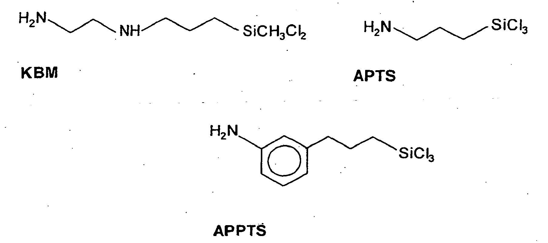
- Halbleiterbauelement nach mindestens einem der vorhergehenden Ansprüche, dadurch gekennzeichnet, dass die Verbindung ein Polyvinylpyrrolidon, ein Pyridilinon oder statistische oder Block-Kopolymere, die diese Einheiten enthalten, ist.
- Verfahren zur Herstellung einer Schichtstruktur in einem Halbleiterbauelement nach mindestens einem der Ansprüche 1 bis 11
dadurch gekennzeichnet, dass
ein Substrat, insbesondere ein Bauelementsubstrat (20) mit einer dielektrischen Schicht (22) in eine Lösung getaucht wird oder aus einer Gasphase abgeschieden wird, die mindestens eine der Verbindungen gemäß Anspruch 1 bis 11 enthält. - Verfahren nach Anspruch 12, dadurch gekennzeichnet, dass die Konzentration der Verbindung in der Lösung zwischen 0,1 und 1% beträgt.
- Verfahren nach Anspruch 13 oder 14, dadurch gekennzeichnet, dass nach dem Aufbringen der Schicht mit der Verbindung (10) nach mindestens einem der Ansprüche 1 bis 11 eine Source-Drain Schicht (23a, 23b) und eine organische Halbleiterschicht (24) aufgebracht wird.
Applications Claiming Priority (2)
| Application Number | Priority Date | Filing Date | Title |
|---|---|---|---|
| DE10332567A DE10332567A1 (de) | 2003-07-11 | 2003-07-11 | Verbindung für die Bildung einer Schicht auf einem Substrat, Verfahren zur Herstellung einer Schicht auf einem Substrat und Halbleiterbauelement |
| PCT/DE2004/001515 WO2005008803A2 (de) | 2003-07-11 | 2004-07-12 | Halbleiterbauelement und verfahren zu dessen herstellung |
Publications (2)
| Publication Number | Publication Date |
|---|---|
| EP1644995A2 EP1644995A2 (de) | 2006-04-12 |
| EP1644995B1 true EP1644995B1 (de) | 2008-04-16 |
Family
ID=34071738
Family Applications (1)
| Application Number | Title | Priority Date | Filing Date |
|---|---|---|---|
| EP04762375A Expired - Lifetime EP1644995B1 (de) | 2003-07-11 | 2004-07-12 | Halbleiterbauelement und verfahren zu dessen herstellung |
Country Status (6)
| Country | Link |
|---|---|
| US (1) | US20060113531A1 (de) |
| EP (1) | EP1644995B1 (de) |
| JP (1) | JP2007507087A (de) |
| CN (1) | CN1823432A (de) |
| DE (2) | DE10332567A1 (de) |
| WO (1) | WO2005008803A2 (de) |
Families Citing this family (5)
| Publication number | Priority date | Publication date | Assignee | Title |
|---|---|---|---|---|
| JP4972870B2 (ja) * | 2005-03-29 | 2012-07-11 | セイコーエプソン株式会社 | 半導体素子の製造方法および半導体装置 |
| DE102005059608B4 (de) * | 2005-12-12 | 2009-04-02 | Polyic Gmbh & Co. Kg | Organisches elektronisches Bauelement mit verbesserter Spannungsstabilität und Verfahren zur Herstellung dazu |
| KR100943146B1 (ko) * | 2007-02-13 | 2010-02-18 | 주식회사 엘지화학 | 티아졸로티아졸 유도체를 이용한 유기 트랜지스터 및 이의제조방법 |
| US8017458B2 (en) * | 2008-01-31 | 2011-09-13 | Northwestern University | Solution-processed high mobility inorganic thin-film transistors |
| US11735593B2 (en) | 2021-11-04 | 2023-08-22 | International Business Machines Corporation | Gate stack dipole compensation for threshold voltage definition in transistors |
Family Cites Families (9)
| Publication number | Priority date | Publication date | Assignee | Title |
|---|---|---|---|---|
| US3705075A (en) * | 1970-12-16 | 1972-12-05 | Owens Corning Fiberglass Corp | Glass fiber reinforced elastomers |
| JPH01240598A (ja) * | 1988-03-18 | 1989-09-26 | Nec Corp | 磁気記憶体およびその製造方法 |
| GB9418289D0 (en) * | 1994-09-10 | 1994-10-26 | Univ Liverpool | Solutions or dispersions and a method of synthesising materials having controlled electronic and optical properties therefrom |
| DE19815220C2 (de) * | 1998-03-27 | 2003-12-18 | Univ Dresden Tech | Verfahren zur haftfesten und dichten chemischen oder galvanischen Metallisierung von Substraten sowie Haftvermittler zur Durchführung des Verfahrens |
| JP2001244383A (ja) * | 2000-02-29 | 2001-09-07 | Sumitomo Bakelite Co Ltd | 半導体装置 |
| DE10025522B4 (de) * | 2000-05-18 | 2004-05-13 | Technische Universität Dresden | Verfahren zur strukturierten Abscheidung leitfähiger Polymerer |
| KR100462712B1 (ko) * | 2000-08-10 | 2004-12-20 | 마쯔시다덴기산교 가부시키가이샤 | 유기전자장치와 그 제조방법과 그 동작방법 및 그것을 사용한 표시장치 |
| JP4839505B2 (ja) * | 2000-10-16 | 2011-12-21 | 日立化成工業株式会社 | 接着フィルム、その製造法及び接着フィルム付き半導体装置 |
| US6710450B2 (en) * | 2001-02-28 | 2004-03-23 | International Business Machines Corporation | Interconnect structure with precise conductor resistance and method to form same |
-
2003
- 2003-07-11 DE DE10332567A patent/DE10332567A1/de not_active Ceased
-
2004
- 2004-07-12 JP JP2006517962A patent/JP2007507087A/ja not_active Abandoned
- 2004-07-12 WO PCT/DE2004/001515 patent/WO2005008803A2/de not_active Ceased
- 2004-07-12 DE DE502004006851T patent/DE502004006851D1/de not_active Expired - Lifetime
- 2004-07-12 EP EP04762375A patent/EP1644995B1/de not_active Expired - Lifetime
- 2004-07-12 CN CNA2004800198407A patent/CN1823432A/zh active Pending
-
2006
- 2006-01-11 US US11/329,695 patent/US20060113531A1/en not_active Abandoned
Also Published As
| Publication number | Publication date |
|---|---|
| JP2007507087A (ja) | 2007-03-22 |
| WO2005008803A3 (de) | 2005-03-10 |
| WO2005008803A2 (de) | 2005-01-27 |
| US20060113531A1 (en) | 2006-06-01 |
| DE10332567A1 (de) | 2005-02-17 |
| CN1823432A (zh) | 2006-08-23 |
| EP1644995A2 (de) | 2006-04-12 |
| DE502004006851D1 (de) | 2008-05-29 |
Similar Documents
| Publication | Publication Date | Title |
|---|---|---|
| EP1636826B1 (de) | Verbindung zur bildung einer selbstorganisierenden monolage, schichtstruktur, halbleiterbauelement mit einer schichtstruktur und verfahren zur herstellung einer schichtstruktur | |
| DE69721929T2 (de) | Tunneleffektanordnung und verfahren zur herstellung | |
| DE102012220731B4 (de) | Verfahren zum Verringern des Kontaktwiderstands für Feldeffekttransistoreinheiten und Vorrichtung | |
| DE102004025423B4 (de) | Dünnfilm-Feldeffekt-Transistor mit Gate-Dielektrikum aus organischem Material und Verfahren zu dessen Herstellung | |
| WO2001011700A1 (de) | Anordnung mit transistor-funktion | |
| DE69132792T2 (de) | Organisches Bauelement und dessen Herstellungsverfahren | |
| DE602004006441T2 (de) | Nichtflüchtiger ferroelektrischer dünnfilm-baustein mit einem organischen ambipolaren halbleiter und verfahren zum verarbeiten eines solchen bausteins | |
| EP1516374A1 (de) | Verringerung des kontaktwiderstandes in organischen feldeffekttransistoren mit palladiumkontakten durch verwendung von nitrilen und isonitrilen | |
| EP1658647B1 (de) | Integrierte schaltung mit einem organischen halbleiter und verfahren zur herstellung einer integrierten schaltung | |
| DE102004022603A1 (de) | Ultradünne Dielektrika und deren Anwendung in organischen Feldeffekt-Transistoren | |
| EP1644995B1 (de) | Halbleiterbauelement und verfahren zu dessen herstellung | |
| EP1563554A2 (de) | Organisches elektronisches bauelement mit gleichem organischem material für zumindest zwei funktionsschichten | |
| WO2005001952A1 (de) | Verbindung zur bildung einer selbstorganisierenden monolage, eine schichtstruktur, ein halbleiterbauelement und ein verfahren zur herstellung einer schichtstruktur | |
| DE102004010094B3 (de) | Halbleiterbauelement mit mindestens einer organischen Halbleiterschicht und Verfahren zu dessen Herstellung | |
| DE10340609A1 (de) | Polymerformulierung und Verfahren zur Herstellung einer Dielektrikumsschicht | |
| DE102004008784B3 (de) | Verfahren zur Durchkontaktierung von Feldeffekttransistoren mit einer selbstorganisierten Monolage einer organischen Verbindung als Gatedielektrikum | |
| DE102004052266A1 (de) | Integrierte Analogschaltung in Schaltkondesatortechnik sowie Verfahren zu deren Herstellung | |
| DE10340610B4 (de) | Verbindung mit mindestens einer Speichereinheit aus organischem Speichermaterial, insbesondere zur Verwendung in CMOS-Strukturen, Halbleiterbauelement und ein Verfahren zur Herstellung eines Halbleiterbauelementes | |
| DE10255870A1 (de) | Verfahren zur Herstellung von organischen Feldeffektransistoren mit Top-Kontakt-Architektur aus leitfähigen Polymeren | |
| DE10361713B4 (de) | Verwendung von Charge-Transfer-Komplexen aus einem Elektronendonor und einem Elektronenakzeptor als Basis für resistive Speicher und Speicherzelle enthaltend diese Komplexe | |
| DE102004040504B4 (de) | Testanordnung für molekulare Bauelemente | |
| DE102004057531A1 (de) | Integrierte Halbleiterspeicherzelle, integrierte Halbleiterspeichereinrichtung und Verfahren zu deren Herstellung | |
| DE102009047315A1 (de) | Organischer Feldeffekttransistor und Verfahren zur Herstellung desselben | |
| DE202005017580U1 (de) | Nano-elektronische Bauelemente | |
| DE102007018800A1 (de) | Elektronisches Bauelement auf der Basis organischer Halbleiter |
Legal Events
| Date | Code | Title | Description |
|---|---|---|---|
| PUAI | Public reference made under article 153(3) epc to a published international application that has entered the european phase |
Free format text: ORIGINAL CODE: 0009012 |
|
| 17P | Request for examination filed |
Effective date: 20051214 |
|
| AK | Designated contracting states |
Kind code of ref document: A2 Designated state(s): DE FR GB |
|
| RIN1 | Information on inventor provided before grant (corrected) |
Inventor name: SCHMID, GUENTER Inventor name: ZSCHIESCHANG, UTE Inventor name: HALIK, MARCUS Inventor name: KLAUK, HAGEN |
|
| 17Q | First examination report despatched |
Effective date: 20060704 |
|
| DAX | Request for extension of the european patent (deleted) | ||
| RBV | Designated contracting states (corrected) |
Designated state(s): DE FR GB |
|
| GRAP | Despatch of communication of intention to grant a patent |
Free format text: ORIGINAL CODE: EPIDOSNIGR1 |
|
| GRAS | Grant fee paid |
Free format text: ORIGINAL CODE: EPIDOSNIGR3 |
|
| GRAA | (expected) grant |
Free format text: ORIGINAL CODE: 0009210 |
|
| AK | Designated contracting states |
Kind code of ref document: B1 Designated state(s): DE FR GB |
|
| RAP1 | Party data changed (applicant data changed or rights of an application transferred) |
Owner name: QIMONDA AG |
|
| RIN1 | Information on inventor provided before grant (corrected) |
Inventor name: ZSCHIESCHANG, UTE Inventor name: SCHMID, GUENTER Inventor name: KLAUK, HAGEN, DR. Inventor name: HALIK, MARCUS |
|
| REF | Corresponds to: |
Ref document number: 502004006851 Country of ref document: DE Date of ref document: 20080529 Kind code of ref document: P |
|
| PGFP | Annual fee paid to national office [announced via postgrant information from national office to epo] |
Ref country code: FR Payment date: 20080715 Year of fee payment: 5 |
|
| ET | Fr: translation filed | ||
| PLBE | No opposition filed within time limit |
Free format text: ORIGINAL CODE: 0009261 |
|
| STAA | Information on the status of an ep patent application or granted ep patent |
Free format text: STATUS: NO OPPOSITION FILED WITHIN TIME LIMIT |
|
| 26N | No opposition filed |
Effective date: 20090119 |
|
| GBPC | Gb: european patent ceased through non-payment of renewal fee |
Effective date: 20080716 |
|
| PG25 | Lapsed in a contracting state [announced via postgrant information from national office to epo] |
Ref country code: GB Free format text: LAPSE BECAUSE OF NON-PAYMENT OF DUE FEES Effective date: 20080716 |
|
| REG | Reference to a national code |
Ref country code: FR Ref legal event code: ST Effective date: 20100331 |
|
| PG25 | Lapsed in a contracting state [announced via postgrant information from national office to epo] |
Ref country code: FR Free format text: LAPSE BECAUSE OF NON-PAYMENT OF DUE FEES Effective date: 20090731 |
|
| REG | Reference to a national code |
Ref country code: DE Ref legal event code: R081 Ref document number: 502004006851 Country of ref document: DE Owner name: INFINEON TECHNOLOGIES AG, DE Free format text: FORMER OWNER: QIMONDA AG, 81739 MUENCHEN, DE Ref country code: DE Ref legal event code: R081 Ref document number: 502004006851 Country of ref document: DE Owner name: POLARIS INNOVATIONS LTD., IE Free format text: FORMER OWNER: QIMONDA AG, 81739 MUENCHEN, DE |
|
| REG | Reference to a national code |
Ref country code: DE Ref legal event code: R081 Ref document number: 502004006851 Country of ref document: DE Owner name: POLARIS INNOVATIONS LTD., IE Free format text: FORMER OWNER: INFINEON TECHNOLOGIES AG, 85579 NEUBIBERG, DE |
|
| PGFP | Annual fee paid to national office [announced via postgrant information from national office to epo] |
Ref country code: DE Payment date: 20160705 Year of fee payment: 13 |
|
| REG | Reference to a national code |
Ref country code: DE Ref legal event code: R119 Ref document number: 502004006851 Country of ref document: DE |
|
| PG25 | Lapsed in a contracting state [announced via postgrant information from national office to epo] |
Ref country code: DE Free format text: LAPSE BECAUSE OF NON-PAYMENT OF DUE FEES Effective date: 20180201 |