EP1645940A2 - Integrierte Schaltungsvorrichtung - Google Patents
Integrierte Schaltungsvorrichtung Download PDFInfo
- Publication number
- EP1645940A2 EP1645940A2 EP05020708A EP05020708A EP1645940A2 EP 1645940 A2 EP1645940 A2 EP 1645940A2 EP 05020708 A EP05020708 A EP 05020708A EP 05020708 A EP05020708 A EP 05020708A EP 1645940 A2 EP1645940 A2 EP 1645940A2
- Authority
- EP
- European Patent Office
- Prior art keywords
- power
- circuit
- processor
- power supply
- integrated circuit
- Prior art date
- Legal status (The legal status is an assumption and is not a legal conclusion. Google has not performed a legal analysis and makes no representation as to the accuracy of the status listed.)
- Withdrawn
Links
Images


Classifications
-
- G—PHYSICS
- G06—COMPUTING OR CALCULATING; COUNTING
- G06F—ELECTRIC DIGITAL DATA PROCESSING
- G06F1/00—Details not covered by groups G06F3/00 - G06F13/00 and G06F21/00
- G06F1/26—Power supply means, e.g. regulation thereof
-
- G—PHYSICS
- G06—COMPUTING OR CALCULATING; COUNTING
- G06F—ELECTRIC DIGITAL DATA PROCESSING
- G06F1/00—Details not covered by groups G06F3/00 - G06F13/00 and G06F21/00
- G06F1/26—Power supply means, e.g. regulation thereof
- G06F1/32—Means for saving power
- G06F1/3203—Power management, i.e. event-based initiation of a power-saving mode
Definitions
- the present invention relates to an integrated circuit device and, particularly, to power control of an integrated circuit.
- LSI large scale integrations
- Various types of large scale integrations (LSI) are incorporated in mobile phones and mobile terminals that are driven by a battery. Reduction of power consumption in LSI is very important factor to enable long time use and achieve multifunction of mobile phones and so on. Further, as LSI becomes more complex, the proportion of static consumption current or leakage current that is consumed in stop state to entire consumption current rises so high that it is not negligible in a microfabrication process of 0.13 ⁇ m or less.
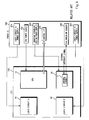
- LSI 100 is connected to a power IC 200.
- the LSI 100 has a central processor unit (CPU) 10, a constant power-on region 20, a logic circuit A 30, and a logic circuit B 40.
- the constant power-on region 20 is a circuit region to which power is supplied constantly in spite that other circuits such as the CPU 10 are not operating.
- the constant power-on region 20 has a control circuit 21 that controls power supply of the CPU 10.
- the control circuit 21 is implemented by a hardware fixed circuit composed of an electric circuit that does not use program and merely executes a fixed operation such as a simple power-on request, for example.
- the power IC 200 is a functional block that has a power supply section 201 for the logic circuit A 30, a power supply section 202 for the CPU 10, a power supply section 203 for the constant power-on region 20, a power supply section 204 for the logic circuit B 40, a control interface (I/F) 205, and a power-on request processing section 206 for the CPU 10.
- a processing operation where an external interrupt signal is input to the control circuit 21 when power supply to the CPU 10 is shut off in the conventional technique shown in Fig. 6 is described hereinafter. Detecting the external interrupt signal, the control circuit 21 sends a request for power supply to the CPU 10 to the power IC 200. Since the CPU 10 in the state where power supply is shut off is initialized, it takes a long boot time when power supply is resumed. For example, a boot time takes as long as 20 to 30 seconds in some cases. Further, since the control circuit 21 is configured by hardware, it can only execute a fixed sequence and cannot deal with a complex power supply sequence.
- control circuit 21 it is difficult for the control circuit 21 to execute a complex power supply sequence of detecting an external interrupt signal, turning on the power of the logic circuit A 30, remaining standby for 50 ⁇ s after executing an initialization routine of the logic circuit A 30, and then turning on the power of the CPU 10. Even if such a complex power supply sequence can be executed by the hardware fixed circuit, it is not possible to execute another power supply sequence without preparation. Furthermore, placing the circuits for executing various types of power supply sequences on a hardware fixed circuit increases the circuit size.
- Japanese Unexamined Patent Publication No. 2002-341976 An example of the conventional power control technique is disclosed in Japanese Unexamined Patent Publication No. 2002-341976.
- the integrated circuit disclosed therein implements CPU power control by a control circuit placed in an I/O terminal.
- this control circuit merely performs very simple control and a backup register also merely performs backup of each signal. Therefore, this control circuit cannot execute a complex power supply sequence and is not flexible.
- Japanese Unexamined Patent Publication No. 2002-288150 Another example of the conventional power control technique is disclosed in Japanese Unexamined Patent Publication No. 2002-288150.
- the integrated circuit disclosed therein has both a high performance CPU and a low power consumption CPU and shuts off the power supply to the CPU that is not operating, thereby reducing leakage current and power consumption.
- the CPU since the CPU has an arithmetic circuit, a considerable amount of leakage current occurs in spite of low power consumption and the effect of reducing power consumption is small.
- the conventional integrated circuit device cannot deal with a complex power supply sequence since it implements CPU power control with a hardware fixed circuit. Further, the conventional technique that implements high performance CPU power control with a low power consumption CPU has only a small power consumption reduction effect.
- an integrated circuit device that includes a processor having an arithmetic circuit and a power management unit implementing power control of the processor through a power supply section without having an arithmetic circuit.
- the power management unit includes a memory storing a plurality of commands and a control section implementing power control of the processor according to the commands stored in the memory. Since this integrated circuit device has the power management unit that implements power control of the processor, it is possible to issue an instruction to each peripheral macro even when no power is supplied to the processor, thereby reducing a time to restart the system.
- the power management unit is programmable, and it is thus possible to execute various power-on/off sequences by changing the commands stored in the memory and to deal with a large number of power division splits. Furthermore, the power management unit allows easy function enhancement and change for command control. In addition, since the power management unit has no arithmetic circuit, the circuit size is significantly smaller than a processor having an arithmetic circuit, thereby achieving low power consumption.
- an integrated circuit device that includes a processor having an arithmetic circuit and a programmable sequencer implementing power control of the processor through a power supply section without having an arithmetic circuit, wherein the programmable sequencer performs initialization of another circuit in the integrated circuit device in parallel with supplying power to the processor through the power supply section.
- the integrated circuit device of this invention has a LSI 100 and a power IC 200, and it is incorporated in a mobile phone, for example, as an application processor.
- the LSI 100 is connected to the power IC 200 that is placed separately from the LSI 100.
- the LSI 100 has a CPU 10, a constant power-on region 20, a logic circuit A 30, and a logic circuit B 40.
- the constant power-on region 20 has a power management unit (PMU) 1 and a clock generation circuit 2.
- the CPU 10 has an arithmetic circuit.
- the CPU 10 and the PMU 1 are connected by a common bus, and signals from the CPU 10 and the PMU 1 are selectively supplied to the power IC 200 through the bus. It is feasible to place a selector for switching signals from the CPU 10 and the PMU 1.
- the PMU 1 has functions to control power supply to the CPU 10, the logic circuit A 30, the logic circuit B 40 and so on and to control operation of the clock generation circuit 2 and a reset control circuit (not shown).
- the PMU 1 has a control section 1a and random access memory (RAM) 1b.
- the control section 1a is configured by an electric circuit that has no arithmetic circuit and operates according to a command sequence or program composed of a plurality of commands stored in the RAM 1b.
- the PMU 1 is a programmable sequencer, which is capable of executing various power on/off sequences by changing the commands stored in the RAM 1b and dealing with a large number of power division splits. Further, the PMU 1 allows easy function enhancement and change for command control.
- the PMU 1 can issue an instruction to each peripheral macro, such as the logic circuit A 30 and the logic circuit B 40 even when no power is supplied to the CPU 10.
- the PMU 1 can control each peripheral macro when power is not supplied to the CPU 10. It is therefore possible to execute various instructions while the CPU 10 performs resume processing after power is supplied to the CPU 10 or before it performs resume processing, thereby reducing a time required to restart the system.
- the PMU 1 has an interrupt monitor function and it can execute power-on sequence in response to input of an external interrupt signal.
- the PMU 1 also has a watchdog timer function and can deal with system hang-up by reset processing.
- the PMU 1 of the first embodiment of the invention is a specialized programmable sequencer for power control and has no arithmetic circuit.
- the PMU 1 has a significantly small size, which is about 1/10 to 1/50, compared with a processor having an arithmetic circuit. Therefore, use of the PMU 1 allows lower power consumption than use of the processor.
- a specific configuration of the PMU 1 is detailed later.
- the clock generation circuit 2 generates and supplies a clock signal to the CPU 10, the logic circuit A 30, the logic circuit B 40 and so on.
- the clock generation circuit 2 is configured by a normal phase lock loop (PLL) circuit and has an oscillator circuit.
- PLL phase lock loop
- the power IC 200 functions as a power supply section that supplies power to the LSI 100.
- the power IC 200 is a functional block that has a power supply section 201 for the logic circuit A 30, a power supply section 202 for the CPU 10, a power supply section 203 for the constant power-on region 20, a power supply section 204 for the logic circuit B 40, and a control interface (I/F) 205.
- the internal block of the PMU 1 is described hereinafter in detail with reference to Fig. 2.
- the PMU 1 has a peripheral macro register interface (I/F) circuit 11, a built-in SRAM 12, a SRAM control/command decode circuit 13, a sequencer circuit 14, and a power control interface (I/F) circuit 15.
- I/F peripheral macro register interface
- the peripheral macro register I/F circuit 11 is connected to the CPU 10, the logic circuit A 30, and the logic circuit B 40 and converts communication protocols in order to perform communication between the CPU 10 and so on and the macros in the PMU 1 such as the built-in SRAM 12 and the sequencer circuit 14.
- the peripheral macro register I/F circuit 11 converts protocols to an I/F bus protocol when transmitting data or command from each macro in the PMU 1 to the CPU 10 or the like.
- the built-in SRAM 12 is a memory that corresponds to the RAM 1b shown in Fig. 1. It is a storage means that stores a command sequence or program composed of a plurality of commands in readable and writable form.
- the SRAM control/command decode circuit 13 controls the built-in SRAM 12.
- the SRAM control/command decode circuit 13 reads out a command stored in the built-in SRAM 12 in response to a command request from the sequencer circuit 14, decodes the command, and outputs it to the sequencer circuit 14.
- the sequencer circuit 14 is composed of a state machine 141 and a decoder 142.
- the sequencer circuit 14 of this invention has no arithmetic circuit.
- the state machine 141 is a circuit that shifts the internal state in synchronization with a command.
- the internal states shifted by the state machine 141 involve an external power-on instruction issue state, a peripheral micro register write state, and an external power stabilization wait state, for example.
- the state machine 141 is configured based on Johnson counter and performs sequence control by changing the internal state sequentially according to external signals.
- the decoder 142 decodes the internal state that is shifted in the state machine 141 to issue an instruction and generate an instruction request signal.
- the power control I/F circuit 15 converts a protocol of an instruction (command) into an I/F bus protocol of the power IC 200 in order to issue the instruction to the power IC 200.
- Steps S1 to S82 shown in the flowchart of Fig. 3 correspond to S1 to S82 shown in Fig. 2, respectively.
- the CPU 10 stores a command into the built-in SRAM 12 (S1, S2). Specifically, the CPU 10 sends a command storage request to the PMU 1 (S1), and the PMU 1 performs protocol conversion on the command storage request by the peripheral macro register I/F circuit 11 and stores the protocol-converted command into a predetermined area of the built-in SRAM 12 (S2).
- the CPU 10 issues an activation request to the PMU 1 (S3).
- the PMU 1 converts the protocol of the activation request by the peripheral macro register I/F circuit 11 and outputs the protocol-converted activation request to the sequencer circuit 14 (S3).
- the sequencer circuit 14 then sends a command request to the SRAM control/command decode circuit 13 in order to perform a processing according to the activation request by the state machine 141 (S4).
- the SRAM control/command decode circuit 13 reads out command data to be processed upon receiving the activation request from the built-in SRAM 12 (S5).
- the SRAM control/command decode circuit 13 receives the read command data, decodes the data and then sends it to the sequencer circuit 14.
- the sequencer circuit 14 writes a predetermined value stored in the built-in SRAM 12 to registers 31 and 41 of the logic circuit A 30 and the logic circuit B 40, respectively, according to the command data.
- the values written to the registers 31 and 41 include a value for changing a clock frequency, a value for reset, and a value for changing modes.
- the sequencer circuit 14 issues an instruction for writing a predetermined value to the registers 31 and 41 and sends it to the peripheral macro register I/F circuit 11 (S72).
- the peripheral macro register I/F circuit 11 converts a protocol of the issued instruction into an I/F bus protocol and sends it to the logic circuits A 30 and B 40 (S82).
- the logic circuits A 30 and B 40 write the predetermined value to the registers 31 and 41, respectively.
- the sequencer circuit 14 sends a power-off instruction to the CPU 10 and the logic circuits A 30 and B 40 through the power IC 200 (S4, S5, S6, S71, S81). Specifically, the state machine 141 of the sequencer circuit 14 requests a command to be processed when receiving a power-off instruction to the SRAM control/command decode circuit 13 (S4). In response to the command request, the SRAM control/command decode circuit 13 reads out the command to be processed when receiving a power-off instruction from the built-in SRAM 12 (S5) and supplies it to the sequencer circuit 14 (S6).
- the sequencer circuit 14 decodes it by the decoder 142 and issues an instruction by the state machine 141 according to the command to be processed when receiving the power-off instruction (S71).
- the instruction in this case is a power-off instruction to the CPU 10 and the logic circuits A 30 and B 40.
- the power control I/F circuit 15 converts the protocol of the issued instruction into a bus protocol and supplies it to the power IC 200 (S81).
- the power IC 200 performs protocol conversion on the power-off instruction by the control I/F 205 and supplies it to the CPU power supply section 202, the logic circuit A power supply section 201, and the logic circuit B power supply section 204.
- the CPU power supply section 202, the logic circuit A power supply section 201, and the logic circuit B power supply section 204 thereby shut off power supply to the CPU 10, the logic circuit A 30, and the logic circuit B 40, respectively.
- Power supply to the CPU 10 and so on stops in response to the power-off instruction and the CPU 10 and so on thereby enter power-off state.
- the PMU 1 waits for power to be stabilized at 0V. Then, the PMU 1 further waits for an external interrupt signal to be input.
- Steps S4 to S82 described in the flowchart of Fig. 4 correspond to S4 to S82 described in Fig. 2, respectively.
- the PMU 1 detects an external interrupt signal when the CPU 10 is in off-state where no power is supplied thereto.
- the sequencer circuit 14 directly detects the external interrupt signal.
- the state machine 141 of the sequencer circuit 14 requests a command to be processed when detecting an external interrupt signal to the SRAM control/command decode circuit 13 (S4).
- the SRAM control/command decode circuit 13 thereby reads out a command corresponding to the command request from the built-in SRAM 12 (S5) and supplies it to the sequencer circuit 14 (S6).
- the sequencer circuit 14 recognizes that the command is a power-on instruction by the decoder 142 and issues a power-on instruction by the state machine 141 (S71).
- the power control I/F circuit 15 converts the protocol of the issued power-on instruction into a path communication protocol and supplies it to the power IC 200 (S81).
- the power IC 200 performs protocol conversion on the power-on instruction by the control I/F 205 and supplies it to the CPU power supply section 202, the logic circuit A power supply section 201, and the logic circuit B power supply section 204.
- the CPU power supply section 202, the logic circuit A power supply section 201, and the logic circuit B power supply section 204 thereby supply power to the CPU 10, the logic circuit A 30, and the logic circuit B 40, respectively.
- the PMU 1 controls power supply so as to supply power only to the area where operation needs to be performed. Therefore, no power is supplied to the area where operation is not performed, thereby saving power consumption.
- the CPU 10 enters power-on state as shown in the flowchart of Fig. 4.
- power of 1.2V is applied to the CPU 10, and the sequencer circuit 14 of the PMU 1 waits for power to be stabilized at 1.2V.
- the state machine 141 of the sequencer circuit 14 writes an initial value to the register 31 of the logic circuit A 30 and the register 41 of the logic circuit B 40.
- the state machine 141 of the sequencer circuit 14 requests a command to the SRAM control/command decode circuit 13 (S4).
- the SRAM control/command decode circuit 13 reads command data from the built-in SRAM 12, decodes the data, and supplies it to the sequencer circuit 14.
- the sequencer circuit 14 decodes the input command by the decoder 142 and issues an instruction (S72). In this case, a command for writing an initial value to the register 31 of the logic circuit A 30 and the register 41 of the logic circuit B 40 is issued. This command contains initial value data.
- the peripheral macro register I/F circuit 11 converts the protocol of the command into a bus communication protocol and supplies it to the logic circuit A 30 and the logic circuit B 40.
- the logic circuit A 30 and the logic circuit B 40 write an initial value to the register 31 and the register 41, respectively, according to the input command.
- the setting of the initial value to the register 31 of the logic circuit A 30 and the register 41 of the logic circuit B 40 is performed by the CPU 10.
- the PMU 1 performs this setting, it is possible to set the initial value before power is supplied to the CPU 10. This allows reduction of a processing time to restart the system.
- the PMU 1 releases reset on the CPU 10 through a reset generation circuit (not shown) placed in the constant power-on region 20.
- the CPU 10 thereby starts resume processing.
- both the CPU 10 and the PMU 1 can perform various processing in parallel during power-on sequence where power supply to the CPU 10 is started, it is possible to reduce a time to restart the system from 20 to 30 seconds to approximately 1 millisecond, for example.
- the integrated circuit of the first embodiment of the invention is incorporated in a mobile phone. If the mobile phone receives a phone call, the PMU 1 controls the power IC 200 so as to supply power to the macro related to phonetic function such as digital signal processor (DSP). It is thereby possible to perform initialization and issue an operation start instruction without waiting for resume processing of the CPU 10 to be finished.
- DSP digital signal processor
- the PMU 1 may issue an instruction to change a clock frequency to the clock generation circuit 2.
- the PMU 1 issues an instruction for changing a clock frequency to be supplied to the CPU 10 from a relatively low frequency to a higher frequency (for example, 200 MHz) to the clock generation circuit 2.
- the clock generation circuit 2 generates a high frequency clock in response to the instruction and supplies it to the CPU 10.
- the clock generation circuit 2 requires 500 microseconds, for example, after changing the frequency until it is stabilized, changing the frequency by the PMU 1 is effective in reducing a time to restart the system.
- the clock generation circuit 2 is placed in the constant power-on region 20 and thus supplied with power; however, the oscillator circuit is in stop state if there is no need to supply a clock to the CPU 10 or the like.
- the PMU 1 of the first embodiment of the invention is programmable, and it is capable of executing various power-on/off sequences by changing commands stored in the RAM 1b and it can deal with a large number of power division splits. Further, the PMU 1 allows easy function enhancement and change for command control.
- the PMU 1 can issue an instruction to each peripheral macro when no power is supplied to the CPU 10. It is therefore possible to execute various instructions while the CPU 10 performs resume processing after power is supplied to the CPU 10 or before it performs resume processing, thereby reducing a time required to restart the system.
- the PMU 1 is a specialized programmable sequencer for power control and has no arithmetic circuit.
- the circuit size is significantly smaller than a processor having an arithmetic circuit, thereby achieving low power consumption.
- a power control technique according to a second embodiment of the invention is described hereinafter with reference to Fig. 5.
- the second embodiment has power supply switches 3a, 3b, 3c, 3d and 3e that correspond to macros placed inside the LSI 100, and the PMU 1 controls on/off of the power switches 3a to 3e.
- the power switches 3a to 3e are placed on branch lines that diverge from a line through which power is supplied constantly from the power IC 200 and are connected to each of the CPU 10 and logic circuits A 30, B 40, C 50 and D 60. Power is supplied from a LSI power supply section 207 of the power IC 200 to the CPU 10 through the power switch 3a. Similarly, power is supplied to the logic circuit A 30 through the power switch 3b, to the logic circuit B 40 through the power switch 3c, to the logic circuit C 50 through the power switch 3d, and to the logic circuit D 60 through the power switch 3e.
- the power switches 3a, 3b, 3c, 3d and 3e are placed in the constant power-on region 20 and on/off controlled by the PMU 1.
- the PMU 1 can perform power control on each macro of the LSI 100 without through the power IC 200, and it is thereby possible to reduce the number of power supplies of the power IC 200 placed outside the LSI 100.
Landscapes
- Engineering & Computer Science (AREA)
- Theoretical Computer Science (AREA)
- Physics & Mathematics (AREA)
- General Engineering & Computer Science (AREA)
- General Physics & Mathematics (AREA)
- Power Sources (AREA)
- Microcomputers (AREA)
Applications Claiming Priority (1)
| Application Number | Priority Date | Filing Date | Title |
|---|---|---|---|
| JP2004292852A JP2006107127A (ja) | 2004-10-05 | 2004-10-05 | 半導体集積回路装置 |
Publications (1)
| Publication Number | Publication Date |
|---|---|
| EP1645940A2 true EP1645940A2 (de) | 2006-04-12 |
Family
ID=35729685
Family Applications (1)
| Application Number | Title | Priority Date | Filing Date |
|---|---|---|---|
| EP05020708A Withdrawn EP1645940A2 (de) | 2004-10-05 | 2005-09-22 | Integrierte Schaltungsvorrichtung |
Country Status (5)
| Country | Link |
|---|---|
| US (1) | US7752467B2 (de) |
| EP (1) | EP1645940A2 (de) |
| JP (1) | JP2006107127A (de) |
| KR (1) | KR100688102B1 (de) |
| CN (1) | CN100354793C (de) |
Cited By (5)
| Publication number | Priority date | Publication date | Assignee | Title |
|---|---|---|---|---|
| WO2008085341A3 (en) * | 2007-01-07 | 2009-01-08 | Apple Inc | Methods and systems for power management in a data processing system |
| US8230124B2 (en) | 2007-08-31 | 2012-07-24 | Apple Inc. | Methods and systems to dynamically manage performance states in a data processing system |
| US8645740B2 (en) | 2007-06-08 | 2014-02-04 | Apple Inc. | Methods and systems to dynamically manage performance states in a data processing system |
| US8667198B2 (en) | 2007-01-07 | 2014-03-04 | Apple Inc. | Methods and systems for time keeping in a data processing system |
| US10564698B2 (en) | 2016-08-19 | 2020-02-18 | Semiconductor Energy Laboratory Co., Ltd. | Method for controlling power supply in semiconductor device |
Families Citing this family (35)
| Publication number | Priority date | Publication date | Assignee | Title |
|---|---|---|---|---|
| JP2006107127A (ja) * | 2004-10-05 | 2006-04-20 | Nec Electronics Corp | 半導体集積回路装置 |
| JP4581933B2 (ja) * | 2005-09-14 | 2010-11-17 | 日本電気株式会社 | 電源供給システム、携帯機器及びそれらに用いる電源投入順序制御方法 |
| US7366926B2 (en) * | 2006-06-13 | 2008-04-29 | Montage Technology Group Limited | On-chip supply regulators |
| JP4685040B2 (ja) | 2007-01-24 | 2011-05-18 | パナソニック株式会社 | 半導体集積回路及びその電源供給制御方法 |
| US7831847B2 (en) * | 2007-05-07 | 2010-11-09 | Mediatek Inc. | Integrated circuit with power control and power control method thereof |
| GB2489344B (en) * | 2007-06-15 | 2012-12-05 | Apple Inc | circuitry and method for regulating a power supply signal |
| US8046615B2 (en) * | 2007-10-19 | 2011-10-25 | Denso Corporation | Microcomputer system with reduced power consumption |
| JP5104254B2 (ja) | 2007-11-30 | 2012-12-19 | 富士通セミコンダクター株式会社 | 集積回路装置 |
| JP2009237712A (ja) * | 2008-03-26 | 2009-10-15 | Fujitsu Ltd | 回路システムおよびプログラム |
| JP2010057160A (ja) * | 2008-08-01 | 2010-03-11 | Nec Electronics Corp | 半導体集積回路 |
| KR101036275B1 (ko) * | 2009-02-03 | 2011-05-23 | 서울대학교산학협력단 | 동작 모니터링 유닛 및 동작 모니터링 유닛을 이용한 시스템의 소비 전력 추정 방법 |
| JP5285643B2 (ja) * | 2010-03-15 | 2013-09-11 | シャープ株式会社 | 半導体集積回路および電子情報機器 |
| US20110307746A1 (en) * | 2010-06-07 | 2011-12-15 | Sullivan Jason A | Systems and Methods for Intelligent and Flexible Management and Monitoring of Computer Systems |
| US8680710B2 (en) * | 2010-12-17 | 2014-03-25 | Texas Instruments Incorporated | Analog power sequencer and method |
| WO2012132020A1 (ja) * | 2011-03-31 | 2012-10-04 | 富士通株式会社 | 情報処理システム、システム管理装置、集積回路 |
| TWI551978B (zh) * | 2011-05-26 | 2016-10-01 | 華碩電腦股份有限公司 | 電腦裝置及其電源產生器 |
| US8769316B2 (en) * | 2011-09-06 | 2014-07-01 | Intel Corporation | Dynamically allocating a power budget over multiple domains of a processor |
| US8954770B2 (en) | 2011-09-28 | 2015-02-10 | Intel Corporation | Controlling temperature of multiple domains of a multi-domain processor using a cross domain margin |
| US9074947B2 (en) | 2011-09-28 | 2015-07-07 | Intel Corporation | Estimating temperature of a processor core in a low power state without thermal sensor information |
| US9026815B2 (en) | 2011-10-27 | 2015-05-05 | Intel Corporation | Controlling operating frequency of a core domain via a non-core domain of a multi-domain processor |
| US8832478B2 (en) | 2011-10-27 | 2014-09-09 | Intel Corporation | Enabling a non-core domain to control memory bandwidth in a processor |
| US9158693B2 (en) | 2011-10-31 | 2015-10-13 | Intel Corporation | Dynamically controlling cache size to maximize energy efficiency |
| US8943340B2 (en) | 2011-10-31 | 2015-01-27 | Intel Corporation | Controlling a turbo mode frequency of a processor |
| US9262133B2 (en) * | 2012-01-27 | 2016-02-16 | Amx Llc | Mapping and formatting input commands to a third party protocol |
| US9229524B2 (en) | 2012-06-27 | 2016-01-05 | Intel Corporation | Performing local power gating in a processor |
| JP2014023235A (ja) * | 2012-07-17 | 2014-02-03 | Ricoh Co Ltd | 電源装置、電源制御方法、及び電源制御プログラム |
| US10079019B2 (en) | 2013-11-12 | 2018-09-18 | Apple Inc. | Always-on audio control for mobile device |
| CN104699212B (zh) * | 2013-12-04 | 2017-11-28 | 联想(北京)有限公司 | 一种电源管理系统、电子设备以及pmu芯片 |
| US10031000B2 (en) | 2014-05-29 | 2018-07-24 | Apple Inc. | System on a chip with always-on processor |
| US9778728B2 (en) | 2014-05-29 | 2017-10-03 | Apple Inc. | System on a chip with fast wake from sleep |
| US9619377B2 (en) | 2014-05-29 | 2017-04-11 | Apple Inc. | System on a chip with always-on processor which reconfigures SOC and supports memory-only communication mode |
| FR3030177B1 (fr) * | 2014-12-16 | 2016-12-30 | Stmicroelectronics Rousset | Dispositif electronique comprenant un module de reveil d'un appareil electronique distinct d'un coeur de traitement |
| JP6068597B2 (ja) * | 2015-11-04 | 2017-01-25 | 株式会社藤商事 | 遊技機 |
| JP2022144020A (ja) * | 2021-03-18 | 2022-10-03 | ローム株式会社 | 電源システム |
| JPWO2023022190A1 (de) * | 2021-08-20 | 2023-02-23 |
Family Cites Families (38)
| Publication number | Priority date | Publication date | Assignee | Title |
|---|---|---|---|---|
| US4097865A (en) * | 1971-06-01 | 1978-06-27 | The United States Of America As Represented By The Secretary Of The Navy | Electronic countermeasure sequence timer |
| US5632037A (en) * | 1992-03-27 | 1997-05-20 | Cyrix Corporation | Microprocessor having power management circuitry with coprocessor support |
| US6343363B1 (en) * | 1994-09-22 | 2002-01-29 | National Semiconductor Corporation | Method of invoking a low power mode in a computer system using a halt instruction |
| US5630143A (en) * | 1992-03-27 | 1997-05-13 | Cyrix Corporation | Microprocessor with externally controllable power management |
| US5455923A (en) * | 1992-07-30 | 1995-10-03 | Kaplinsky; Cecil H. | Memory system for loading peripherals on power up |
| EP0654726B1 (de) * | 1993-11-23 | 1998-12-16 | Advanced Micro Devices, Inc. | Leistungssteuerungssysteme für Rechner |
| US5596756A (en) * | 1994-07-13 | 1997-01-21 | Advanced Micro Devices, Inc. | Sub-bus activity detection technique for power management within a computer system |
| US5784611A (en) * | 1994-12-19 | 1998-07-21 | Seagate Technology, Inc. | Device and process for in-system programming electrically erasable and programmable non-volatile memory |
| JP3188840B2 (ja) * | 1996-06-14 | 2001-07-16 | インターナショナル・ビジネス・マシーンズ・コーポレ−ション | コンピュータ・システムに用いられる周辺装置及びその制御方法 |
| US6230278B1 (en) * | 1997-05-02 | 2001-05-08 | Texas Instruments Incorporated | Microprocessor with functional units that can be selectively coupled |
| CN1157641C (zh) * | 1997-09-03 | 2004-07-14 | 松下电器产业株式会社 | 处理器 |
| KR100382636B1 (ko) * | 1998-07-15 | 2005-09-20 | 삼성전자주식회사 | 컴퓨터의냉각팬제어장치 |
| JP2000112585A (ja) * | 1998-10-02 | 2000-04-21 | Toshiba Corp | システムlsi及びパワーマネジメント方法 |
| JP4272743B2 (ja) * | 1999-04-01 | 2009-06-03 | ハセガワ株式会社 | 剣道面防具 |
| US6510525B1 (en) * | 1999-04-26 | 2003-01-21 | Mediaq, Inc. | Method and apparatus to power up an integrated device from a low power state |
| JP2000341976A (ja) * | 1999-05-31 | 2000-12-08 | Takata Corp | 磁性流体伝動機構及びそれを用いた超音波駆動装置 |
| US6636962B1 (en) * | 1999-12-10 | 2003-10-21 | Intel Corporation | Self-initializing chipset |
| US6640262B1 (en) * | 1999-12-20 | 2003-10-28 | 3Com Corporation | Method and apparatus for automatically configuring a configurable integrated circuit |
| KR20020014534A (ko) * | 2000-08-18 | 2002-02-25 | 박종섭 | 저전력 오디오 프로세서 |
| US6772360B2 (en) * | 2001-02-07 | 2004-08-03 | Emulex Design & Manufacturing Corporation | Extension signal generator coupled to an extension timer and an extension register to generate an initialization extension signal |
| JP3480721B2 (ja) * | 2001-02-22 | 2003-12-22 | Necパーソナルプロダクツ株式会社 | 電源オン/オフシーケンス制御装置 |
| JP2002288150A (ja) * | 2001-03-28 | 2002-10-04 | Matsushita Electric Ind Co Ltd | 半導体集積回路装置 |
| JP2002341976A (ja) * | 2001-05-15 | 2002-11-29 | Matsushita Electric Ind Co Ltd | 多電源半導体装置及び該装置の電源制御方法 |
| JP2003132683A (ja) * | 2001-10-23 | 2003-05-09 | Hitachi Ltd | 半導体装置 |
| JP4434539B2 (ja) * | 2001-12-26 | 2010-03-17 | 富士通マイクロエレクトロニクス株式会社 | プロセッサおよびそのブート方法 |
| JP2003202935A (ja) * | 2002-01-08 | 2003-07-18 | Mitsubishi Electric Corp | 電力管理方式及び電力管理方法 |
| US7191350B2 (en) * | 2002-01-30 | 2007-03-13 | Matsushita Electric Industrial Co., Ltd. | Instruction conversion apparatus and instruction conversion method providing power control information, program and circuit for implementing the instruction conversion, and microprocessor for executing the converted instruction |
| US20030233534A1 (en) * | 2002-06-12 | 2003-12-18 | Adrian Bernhard | Enhanced computer start-up methods |
| JP4048091B2 (ja) * | 2002-09-17 | 2008-02-13 | 株式会社リコー | Lsi及び画像形成装置 |
| JP4038134B2 (ja) * | 2003-02-05 | 2008-01-23 | インターナショナル・ビジネス・マシーンズ・コーポレーション | 電源制御装置及び情報処理装置 |
| US7062668B2 (en) * | 2003-04-24 | 2006-06-13 | Dell Products L.P. | Method and system for information handling system component power management sequencing |
| US7170315B2 (en) * | 2003-07-31 | 2007-01-30 | Actel Corporation | Programmable system on a chip |
| US7376854B2 (en) * | 2004-03-31 | 2008-05-20 | Intel Corporation | System for enabling and disabling voltage regulator controller of electronic appliance according to a series of delay times assigned to voltage regulator controllers |
| JP2005309957A (ja) * | 2004-04-23 | 2005-11-04 | Denso Corp | マイクロコンピュータ、車載システム |
| US7519802B2 (en) * | 2004-05-05 | 2009-04-14 | Hewlett-Packard Development Company, L.P. | System and method for configuring a computer system |
| US7210030B2 (en) * | 2004-07-22 | 2007-04-24 | International Business Machines Corporation | Programmable memory initialization system and method |
| US7266680B1 (en) * | 2004-07-29 | 2007-09-04 | Marvell International Ltd. | Method and apparatus for loading configuration data |
| JP2006107127A (ja) * | 2004-10-05 | 2006-04-20 | Nec Electronics Corp | 半導体集積回路装置 |
-
2004
- 2004-10-05 JP JP2004292852A patent/JP2006107127A/ja active Pending
-
2005
- 2005-09-21 KR KR1020050087770A patent/KR100688102B1/ko not_active Expired - Fee Related
- 2005-09-22 EP EP05020708A patent/EP1645940A2/de not_active Withdrawn
- 2005-09-27 CN CNB200510107091XA patent/CN100354793C/zh not_active Expired - Fee Related
- 2005-10-04 US US11/242,045 patent/US7752467B2/en not_active Expired - Fee Related
Cited By (10)
| Publication number | Priority date | Publication date | Assignee | Title |
|---|---|---|---|---|
| WO2008085341A3 (en) * | 2007-01-07 | 2009-01-08 | Apple Inc | Methods and systems for power management in a data processing system |
| US7917784B2 (en) | 2007-01-07 | 2011-03-29 | Apple Inc. | Methods and systems for power management in a data processing system |
| US8145928B2 (en) | 2007-01-07 | 2012-03-27 | Apple Inc. | Methods and systems for power management in a data processing system |
| US8473764B2 (en) | 2007-01-07 | 2013-06-25 | Apple Inc. | Methods and systems for power efficient instruction queue management in a data processing system |
| US8667198B2 (en) | 2007-01-07 | 2014-03-04 | Apple Inc. | Methods and systems for time keeping in a data processing system |
| US8762755B2 (en) | 2007-01-07 | 2014-06-24 | Apple Inc. | Methods and systems for power management in a data processing system |
| US8645740B2 (en) | 2007-06-08 | 2014-02-04 | Apple Inc. | Methods and systems to dynamically manage performance states in a data processing system |
| US8230124B2 (en) | 2007-08-31 | 2012-07-24 | Apple Inc. | Methods and systems to dynamically manage performance states in a data processing system |
| US10564698B2 (en) | 2016-08-19 | 2020-02-18 | Semiconductor Energy Laboratory Co., Ltd. | Method for controlling power supply in semiconductor device |
| US11281285B2 (en) | 2016-08-19 | 2022-03-22 | Semiconductor Energy Laboratory Co., Ltd. | Method for controlling power supply in semiconductor device |
Also Published As
| Publication number | Publication date |
|---|---|
| US7752467B2 (en) | 2010-07-06 |
| KR20060051490A (ko) | 2006-05-19 |
| KR100688102B1 (ko) | 2007-03-02 |
| CN1758183A (zh) | 2006-04-12 |
| JP2006107127A (ja) | 2006-04-20 |
| CN100354793C (zh) | 2007-12-12 |
| US20060075267A1 (en) | 2006-04-06 |
Similar Documents
| Publication | Publication Date | Title |
|---|---|---|
| US7752467B2 (en) | Integrated circuit device | |
| TW573245B (en) | CPU powerdown method and apparatus therefor | |
| US5561384A (en) | Input/output driver circuit for isolating with minimal power consumption a peripheral component from a core section | |
| US5898232A (en) | Input/output section of an integrated circuit having separate power down capability | |
| US20030070065A1 (en) | Suspending to nonvolatile storage | |
| KR20060087826A (ko) | 절전모드가 아닌 동작상태저장과 전원차단으로 구현하는시스템의 소비전력 감소 방법 및 장치 | |
| WO2011033626A1 (ja) | コンピュータシステム | |
| US7219248B2 (en) | Semiconductor integrated circuit operable to control power supply voltage | |
| JP3070527B2 (ja) | 無線携帯端末 | |
| US7848718B2 (en) | Method apparatus comprising integrated circuit and method of powering down such circuit | |
| CN111142653A (zh) | 一种PCIe设备低功耗控制方法、装置及电子设备 | |
| JP2004070854A (ja) | データプロセッサ | |
| US8296592B2 (en) | Semiconductor integrated circuit | |
| JPH06230845A (ja) | レジューム方式 | |
| KR101236393B1 (ko) | 전자장치 및 그 제어방법 | |
| JPH04167113A (ja) | 情報処理装置 | |
| US20060215288A1 (en) | Image forming apparatus with power-saving mode | |
| JP2008191840A (ja) | 制御システム及び制御方法 | |
| KR20050000233A (ko) | 컴퓨터의 절전시스템 및 절전방법 | |
| JPH11353161A (ja) | 制御プログラムの起動方法 | |
| JPH06223028A (ja) | サスペンド・レジューム制御装置 | |
| JPH0736576A (ja) | コンピュータシステム | |
| JP2014071481A (ja) | 半導体装置 |
Legal Events
| Date | Code | Title | Description |
|---|---|---|---|
| PUAI | Public reference made under article 153(3) epc to a published international application that has entered the european phase |
Free format text: ORIGINAL CODE: 0009012 |
|
| AK | Designated contracting states |
Kind code of ref document: A2 Designated state(s): AT BE BG CH CY CZ DE DK EE ES FI FR GB GR HU IE IS IT LI LT LU LV MC NL PL PT RO SE SI SK TR |
|
| AX | Request for extension of the european patent |
Extension state: AL BA HR MK YU |
|
| RAP1 | Party data changed (applicant data changed or rights of an application transferred) |
Owner name: RENESAS ELECTRONICS CORPORATION |
|
| RAP1 | Party data changed (applicant data changed or rights of an application transferred) |
Owner name: RENESAS ELECTRONICS CORPORATION |
|
| RIC1 | Information provided on ipc code assigned before grant |
Ipc: G06F 1/32 20060101AFI20160317BHEP |
|
| STAA | Information on the status of an ep patent application or granted ep patent |
Free format text: STATUS: THE APPLICATION HAS BEEN WITHDRAWN |
|
| 18W | Application withdrawn |
Effective date: 20160418 |