EP1646066A2 - Plasmaanzeigetafel und Plasmaanzeigevorrichtung mit Elektroden - Google Patents
Plasmaanzeigetafel und Plasmaanzeigevorrichtung mit Elektroden Download PDFInfo
- Publication number
- EP1646066A2 EP1646066A2 EP05256319A EP05256319A EP1646066A2 EP 1646066 A2 EP1646066 A2 EP 1646066A2 EP 05256319 A EP05256319 A EP 05256319A EP 05256319 A EP05256319 A EP 05256319A EP 1646066 A2 EP1646066 A2 EP 1646066A2
- Authority
- EP
- European Patent Office
- Prior art keywords
- electrode part
- center
- plasma display
- discharge
- main electrodes
- Prior art date
- Legal status (The legal status is an assumption and is not a legal conclusion. Google has not performed a legal analysis and makes no representation as to the accuracy of the status listed.)
- Withdrawn
Links
Images
Classifications
-
- H—ELECTRICITY
- H01—ELECTRIC ELEMENTS
- H01J—ELECTRIC DISCHARGE TUBES OR DISCHARGE LAMPS
- H01J11/00—Gas-filled discharge tubes with alternating current induction of the discharge, e.g. alternating current plasma display panels [AC-PDP]; Gas-filled discharge tubes without any main electrode inside the vessel; Gas-filled discharge tubes with at least one main electrode outside the vessel
- H01J11/10—AC-PDPs with at least one main electrode being out of contact with the plasma
- H01J11/12—AC-PDPs with at least one main electrode being out of contact with the plasma with main electrodes provided on both sides of the discharge space
-
- H—ELECTRICITY
- H01—ELECTRIC ELEMENTS
- H01J—ELECTRIC DISCHARGE TUBES OR DISCHARGE LAMPS
- H01J11/00—Gas-filled discharge tubes with alternating current induction of the discharge, e.g. alternating current plasma display panels [AC-PDP]; Gas-filled discharge tubes without any main electrode inside the vessel; Gas-filled discharge tubes with at least one main electrode outside the vessel
- H01J11/20—Constructional details
- H01J11/22—Electrodes, e.g. special shape, material or configuration
- H01J11/24—Sustain electrodes or scan electrodes
-
- H—ELECTRICITY
- H01—ELECTRIC ELEMENTS
- H01J—ELECTRIC DISCHARGE TUBES OR DISCHARGE LAMPS
- H01J11/00—Gas-filled discharge tubes with alternating current induction of the discharge, e.g. alternating current plasma display panels [AC-PDP]; Gas-filled discharge tubes without any main electrode inside the vessel; Gas-filled discharge tubes with at least one main electrode outside the vessel
- H01J11/20—Constructional details
- H01J11/22—Electrodes, e.g. special shape, material or configuration
- H01J11/32—Disposition of the electrodes
-
- H—ELECTRICITY
- H01—ELECTRIC ELEMENTS
- H01J—ELECTRIC DISCHARGE TUBES OR DISCHARGE LAMPS
- H01J2211/00—Plasma display panels with alternate current induction of the discharge, e.g. AC-PDPs
- H01J2211/20—Constructional details
- H01J2211/22—Electrodes
- H01J2211/24—Sustain electrodes or scan electrodes
- H01J2211/245—Shape, e.g. cross section or pattern
-
- H—ELECTRICITY
- H01—ELECTRIC ELEMENTS
- H01J—ELECTRIC DISCHARGE TUBES OR DISCHARGE LAMPS
- H01J2211/00—Plasma display panels with alternate current induction of the discharge, e.g. AC-PDPs
- H01J2211/20—Constructional details
- H01J2211/22—Electrodes
- H01J2211/32—Disposition of the electrodes
- H01J2211/323—Mutual disposition of electrodes
Definitions
- the present invention relates to a plasma display panel and a plasma display apparatus. It more particularly relates to a plasma display panel and plasma display apparatus comprising electrodes.
- a known type of plasma display panel comprises a front substrate and a rear substrate comprised of soda-lime glass. Barrier ribs formed between the front substrate and the rear substrate partition discharge cells.
- An inert gas injected into the discharge cells such as helium-xeon (He-Xe) or helium-neon (He-Ne), generates a discharge with a high frequency voltage.
- He-Xe helium-xeon
- He-Ne helium-neon
- Vacuum ultraviolet rays excite phosphors formed between the barrier ribs, thus displaying images.
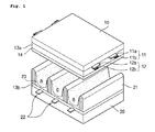
- FIG. 1 is a perspective view schematically showing the construction of a conventional plasma display panel.
- the conventional plasma display panel comprises a front panel and a rear panel.
- the front panel comprises a front glass substrate 10.
- the rear panel comprises a rear glass substrate 20.
- the front panel and the rear panel are parallel to each other with a predetermined gap therebetween.
- the sustain electrode pair comprises the scan electrodes 11 and the sustain electrodes 12.
- the scan electrode 11 comprises a transparent electrode 11a formed of a transparent ITO material and a bus electrode 11b formed of a metal material.
- the sustain electrode 12 comprises a transparent electrode 12a formed of a transparent ITO material and a bus electrode 12b formed of a metal material.
- the scan electrode 11 receives a scan signal for scanning a panel and a sustain signal for sustaining a discharge.
- the sustain electrode 12 mainly receives a sustain signal.
- a dielectric layer 13a is formed on the sustain electrode pair 11 and 12, and functions to limit the discharge current and provide insulation between the electrode pairs.
- a protection layer 14 is formed of magnesium oxide (MgO) on a top surface of the dielectric layer 13a so as to facilitate a discharge.
- MgO magnesium oxide
- Address electrodes 22 intersecting the sustain electrode pair 11 and 12 are disposed on the rear glass substrate 20.
- a dielectric layer 13b formed on the address electrodes 22 functions to provide insulation between the address electrodes 22.
- Barrier ribs 21 formed on the dielectric layer 13b partition discharge cells.
- R, G and B phosphor layer 23 coated between the barrier ribs 21 and the barrier ribs 21 radiate a visible ray for displaying images.
- the front glass substrate 10 and the rear glass substrate 20 are combined together by a sealing material.
- An inert gas such as helium (He), neon (Ne) or xeon (Xe), is injected into the plasma display panel on which an exhaust process has been performed.
- the conventional plasma display panel is subject to increased manufacturing cost given that such panels comprise expensive transparent electrodes.
- a fence type electrode structure to be used instead of the transparent electrodes has been proposed.
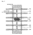
- FIG. 2 is a plan view of a discharge cell having the fence type electrode structure of the conventional plasma display panel.
- a plurality of scan bus electrodes 210 and a plurality of sustain bus electrodes 220 are formed on upper and lower sides of the panel within a discharge space without expensive transparent electrodes.
- a scan connection electrode 230 connecting the plurality of scan bus electrodes 210 and a sustain connection electrode 240 connecting the plurality of sustain bus electrodes 220 are formed in the plasma display panel.
- the scan bus electrodes 210 connected by the scan connection electrode 230 and the sustain bus electrodes 210 connected by the sustain connection electrode 240 are separated from each other with a predetermined gap therebetween, and thus form a discharge gap 250.
- a discharge can be generated without expensive transparent electrodes. Since a discharge is performed through opaque bus electrodes, however, the aperture ratio is reduced. Furthermore, since these opaque bus electrodes are all formed within the discharge space, the aperture ratio is reduced even further.
- the area in which the discharge space and the fence type bus electrodes overlap with each other is less than the area in which the discharge space and the transparent electrodes 11a and 12a of FIG. 1 overlap with each other. As a result, problems arise that the discharge amount is small and a discharge does not diffuse into the entire discharge space.
- the problems of the low aperture ratio and poor discharge diffusion in the conventional fence type electrode structure result in an increased discharge sustain voltage of the plasma display panel and decreased brightness and discharge efficiency.
- the present invention seeks to provide an improved plasma display apparatus.
- a plasma display panel comprises a discharge cell partitioned by barrier ribs, an upper electrode part comprising a plurality of upper main electrodes and an upper connection electrode part that connects each of the plurality of upper main electrodes, and formed on an upper region of the discharge cell, a lower electrode part comprising a plurality of lower main electrodes and a lower connection electrode part that connects each of the plurality of lower main electrodes, and formed on a lower region of the discharge cell, a first center electrode part comprising a plurality of first center main electrodes and a first center connection electrode part that connects each of the plurality of first center main electrodes, and formed between the upper electrode part and the lower electrode part and a second center electrode part comprising a plurality of second center main electrodes and a second center connection electrode part that connects each of the plurality of second center main electrodes, and formed between the first center electrode part and the lower electrode part.
- the upper electrode part and the lower electrode part may function as a scan electrode and the first center electrode part and the second center electrode part may function as a sustain electrode, and the upper electrode part and the lower electrode part may function as the sustain electrode and the first center electrode part and the second center electrode part may function as the scan electrode.
- the upper electrode part and the first center electrode part may form a first discharge gap.
- the lower electrode part and the second center electrode part may form a second discharge gap.
- the first center electrode part and the second center electrode part may be separated from each other.
- a gap between the first center electrode part and the second center electrode part may be equal to or greater than 50 ⁇ m to less than or equal to 200 ⁇ m.
- At least one of the upper connection electrode part, the lower connection electrode part, the first center connection electrode part and the second center connection electrode part may comprise one or more connection electrodes.
- the width of at least one of the upper main electrode, the lower main electrode, the first center main electrode and the second center main electrode may be equal to or greater than 30 ⁇ m to less than or equal to 60 ⁇ m.
- a plasma display apparatus comprises a discharge cell partitioned by barrier ribs, an upper electrode part comprising a plurality of upper main electrodes and an upper connection electrode part that connects each of the plurality of upper main electrodes, and formed on an upper region of the discharge cell, a lower electrode part comprising a plurality of lower main electrodes and a lower connection electrode part that connects each of the plurality of lower main electrodes, and formed on a lower region of the discharge cell, a first center electrode part comprising a plurality of first center main electrodes and a first center connection electrode part that connects each of the plurality of first center main electrodes, and formed between the upper electrode part and the lower electrode part, a second center electrode part comprising a plurality of second center main electrodes and a second center connection electrode part that connects each of the plurality of second center main electrodes, and formed between the first center electrode part and the lower electrode part, a first driver that applies first driving pulses to the upper electrode part and the lower electrode part and a
- the first driver may apply the first driving pulses to the upper electrode part and the lower electrode part so that the upper electrode part and the lower electrode part function as a scan electrode
- the second driver may apply the second driving pulses to the first center electrode part and the second center electrode part so that the first center electrode part and the second center electrode part function as a sustain electrode
- the first driver may apply the first driving pulses to the upper electrode part and the lower electrode part so that the upper electrode part and the lower electrode part function as a sustain electrode
- the second driver may apply the second driving pulses to the first center electrode part and the second center electrode part so that the first center electrode part and the second center electrode part function as a acan electrode
- the first center electrode part and the second center electrode part may be separated from each other.
- a gap between the first center electrode part and the second center electrode part may be equal to or greater than 50 ⁇ m to less than or equal to 200 ⁇ m.
- FIG. 1 is a perspective view schematically showing the construction of a prior art plasma display panel
- FIG. 2 is a plan view of a discharge cell having the fence type electrode structure of the prior art plasma display panel
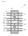
- FIG. 3 is a plan view of a plasma display panel according to the present invention.
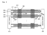
- FIG. 4 shows the construction of a plasma display apparatus according to the present invention.
- the plasma display panel comprises a discharge cell 290, an upper electrode part 310, a lower electrode part 320, a first center electrode part 330 and a second center electrode part 340.
- the discharge cell 290 is partitioned by a barrier rib 295.
- the upper electrode part 310 comprises a plurality of upper main electrodes 311 and 313 and an upper connection electrode part 315 that connects each of the plurality of upper main electrodes 311 and 313.
- the upper electrode part 310 is formed on an upper region of the discharge cell 290.
- the upper connection electrode part 315 comprises one upper connection electrode.
- the upper connection electrode part 315 can comprise a plurality of upper connection electrodes.
- the plurality of upper main electrodes 311,313 and the upper connection electrode part 315 are bus electrodes.
- the width of each of the upper main electrodes 311,313 is equal to or greater than 30 ⁇ m to less than or equal to 60 ⁇ m.
- the lower electrode part 320 comprises a plurality of lower main electrodes 321 and 323 and a lower connection electrode part 325 that connects each of the plurality of lower main electrodes 321 and 323.
- the lower electrode part 320 is formed on a lower region of the discharge cell 290.
- the lower connection electrode part 325 comprises one lower connection electrode.
- the lower connection electrode part 325 can comprise a plurality of lower connection electrodes.
- the plurality of lower main electrodes 321 and 323 and the lower connection electrode part 325 are bus electrodes.
- the width of each of the lower main electrodes 321 and 323 is equal to or greater than 30 ⁇ m to less than or equal to 60 ⁇ m.
- the first center electrode part 330 comprises a plurality of first center main electrodes 331 and 333 and a first center connection electrode part 335 that connects each of the plurality of first center main electrodes 331 and 333, and is formed between the upper electrode part 310 and the lower electrode part 320.
- the first center connection electrode part 335 comprises one first center connection electrode.
- the first center connection electrode part 335 can comprise a plurality of first center connection electrodes.
- the plurality of first center main electrodes 331 and 333 and the first center connection electrode part 335 are bus electrodes.
- the width of each of the first center main electrodes 331 and 333 is equal to or greater than 30 ⁇ m to less than or equal to 0 ⁇ m.
- the second center electrode part 340 comprises a plurality of second center main electrodes 341 and 343 and a second center connection electrode part 345 that connects each of the plurality of second center main electrodes 341 and 343.
- the second center electrode part 340 is formed between the first center electrode part 330 and the lower electrode part 320.
- the second center connection electrode part 345 comprises a second center connection electrode.
- the second center connection electrode part 345 can comprise a plurality of second center connection electrodes.
- the plurality of second center main electrodes 341 and 343 and the second center connection electrode part 345 are bus electrodes.
- the width of each of the second center main electrodes 341 and 343 is equal to or greater than 30 ⁇ m to less than or equal to 60 ⁇ m.
- the first center electrode part and the second center electrode part function as a sustain electrode.
- the first center electrode part and the second center electrode part function as the scan electrode.
- two discharge gaps 350 and 360 are formed within the discharge cell 290. That is, the upper electrode part 310 and the first center electrode part 330 form the first discharge gap 350, and the lower electrode part 320 and the second center electrode part 340 form the second discharge gap 360.
- the plurality of discharge gaps 350 and 360 are formed in one discharge cell 290, thus increasing the discharge amount.
- connection electrode parts 315,325,335 and 345 and the main electrodes 311,313,321,323,331,333,341 and 343, which are comprised in the electrode parts 310,320,330 and340, function to diffuse a discharge generated in the two discharge gaps 350 and 360 into the entire region of the discharge cell 290. Therefore, the plasma display panel of the present invention increases the discharge amount and facilitates discharge diffusion, so that discharge efficiency will be increased. Accordingly, the plasma display panel can decrease a discharge sustain voltage and can increase brightness and discharge efficiency.
- the plurality of discharge gaps 350 and 360 are formed on the upper and lower sides of the discharge cell 290, respectively, a sufficient amount of wall charges can be accumulated on each electrode.
- the first center electrode part 330 and the second center electrode part 340 of the present invention can be separated from each other.
- the dimensions of a gap 370 between the first center electrode part 330 and the second center electrode part 340 ranges from equal to or greater than 50 ⁇ m to less than or equal to 200 ⁇ m.
- a discharge generated in the first discharge gap 350 has an effect on a discharge generated in the second discharge gap 360. That is, although the two discharge gaps 350 and 360 have the same design value, a discharge that is first generated by the distribution of wall charges influences subsequently generated discharge.
- first center electrode part 330 and the second center electrode part 340 are separated from each other, as shown in FIG. 3.
- a plasma display apparatus comprises a discharge cell 290, an upper electrode part 310, a lower electrode part 320, a first center electrode part 330, a second center electrode part 340, a first driver 410 and a second driver 420.
- the discharge cell 290, the upper electrode part 310, the lower electrode part 320, the first center electrode part 330 and the second center electrode part 340 have the same construction as that described above. Detailed description thereof will be omitted.
- the first driver 410 applies first driving pulses to the upper electrode part 310 and the lower electrode part 320.
- the second driver 420 applies second driving pulses to the first center electrode part 330 and the second center electrode part 340.
- the first driver 410 applies the first driving pulses, such as a reset pulse, a scan pulse and a sustain pulse, to the upper electrode part 310 and the lower electrode part 320, the upper electrode part 310 and the lower electrode part 320 function as a scan electrode.
- the second driver 420 applies the second driving pulses to the first center electrode part 330 and the second center electrode part 340 so that the first center electrode part 330 and the second center electrode part 340 function as the sustain electrodes.
- the second driver 420 applies the first driving pulses, such as a reset pulse, a scan pulse and a sustain pulse, to the first center electrode part 330 and the second center electrode part 340, the first center electrode part 330 and the second center electrode part 340 serve as scan electrodes.
- the second driver 420 applies the second driving pulses to the upper electrode part 310 and the lower electrode part 320 so that the upper electrode part 310 and the lower electrode part 320 serve as the sustain electrodes.
- the first center electrode part 330 and the second center electrode part 340 of the present invention are separated from each other.
- the dimension of the gap 370 between the first center electrode part 330 and the second center electrode part 340 lies in the range equal to or greater than 50 ⁇ m to less than or equal to 200 ⁇ m.
Landscapes
- Engineering & Computer Science (AREA)
- Physics & Mathematics (AREA)
- Plasma & Fusion (AREA)
- Chemical & Material Sciences (AREA)
- Materials Engineering (AREA)
- Gas-Filled Discharge Tubes (AREA)
Applications Claiming Priority (1)
| Application Number | Priority Date | Filing Date | Title |
|---|---|---|---|
| KR1020040081129A KR100680770B1 (ko) | 2004-10-11 | 2004-10-11 | 스캔 전극과 서스테인 전극을 포함하는 플라즈마디스플레이 패널 |
Publications (2)
| Publication Number | Publication Date |
|---|---|
| EP1646066A2 true EP1646066A2 (de) | 2006-04-12 |
| EP1646066A3 EP1646066A3 (de) | 2008-09-17 |
Family
ID=36144565
Family Applications (1)
| Application Number | Title | Priority Date | Filing Date |
|---|---|---|---|
| EP05256319A Withdrawn EP1646066A3 (de) | 2004-10-11 | 2005-10-11 | Plasmaanzeigetafel und Plasmaanzeigevorrichtung mit Elektroden |
Country Status (5)
| Country | Link |
|---|---|
| US (1) | US20060076876A1 (de) |
| EP (1) | EP1646066A3 (de) |
| JP (1) | JP2006114497A (de) |
| KR (1) | KR100680770B1 (de) |
| CN (1) | CN1761020A (de) |
Family Cites Families (7)
| Publication number | Priority date | Publication date | Assignee | Title |
|---|---|---|---|---|
| US6411035B1 (en) * | 1999-05-12 | 2002-06-25 | Robert G. Marcotte | AC plasma display with apertured electrode patterns |
| KR100880774B1 (ko) * | 2000-01-25 | 2009-02-02 | 파나소닉 주식회사 | 가스방전패널 |
| KR100891585B1 (ko) * | 2000-08-18 | 2009-04-03 | 파나소닉 주식회사 | 가스방전패널 |
| CN100409394C (zh) * | 2000-08-29 | 2008-08-06 | 松下电器产业株式会社 | 气体放电屏 |
| US6614182B2 (en) * | 2000-12-28 | 2003-09-02 | Nec Corporation | Plasma display panel |
| KR20040051289A (ko) * | 2002-12-12 | 2004-06-18 | 현대 프라즈마 주식회사 | 투명전극이 없는 플라즈마 디스플레이 패널 |
| TWI224349B (en) * | 2003-06-13 | 2004-11-21 | Chunghwa Picture Tubes Ltd | Electrode structure of plasma display panel |
-
2004
- 2004-10-11 KR KR1020040081129A patent/KR100680770B1/ko not_active Expired - Fee Related
-
2005
- 2005-10-11 JP JP2005296214A patent/JP2006114497A/ja not_active Withdrawn
- 2005-10-11 US US11/246,120 patent/US20060076876A1/en not_active Abandoned
- 2005-10-11 EP EP05256319A patent/EP1646066A3/de not_active Withdrawn
- 2005-10-11 CN CNA2005101085987A patent/CN1761020A/zh active Pending
Also Published As
| Publication number | Publication date |
|---|---|
| JP2006114497A (ja) | 2006-04-27 |
| CN1761020A (zh) | 2006-04-19 |
| US20060076876A1 (en) | 2006-04-13 |
| KR20060032108A (ko) | 2006-04-14 |
| KR100680770B1 (ko) | 2007-02-09 |
| EP1646066A3 (de) | 2008-09-17 |
Similar Documents
| Publication | Publication Date | Title |
|---|---|---|
| JP3121247B2 (ja) | Ac型プラズマディスプレイパネルおよび駆動方法 | |
| JP2000251745A (ja) | プラズマディスプレイパネル | |
| KR100659064B1 (ko) | 플라즈마 디스플레이 패널 | |
| US7535177B2 (en) | Plasma display panel having electrodes arranged within barrier ribs | |
| KR100854879B1 (ko) | 한쌍의 라인전극 상에 위치하는 복수의 셀 내에서 방전을실행하는 패널 | |
| EP1646065A2 (de) | Plasmaanzeigetafel und Plasmaanzeigevorrichtung mit Elektroden | |
| US7135819B2 (en) | Plasma display panel | |
| EP1646066A2 (de) | Plasmaanzeigetafel und Plasmaanzeigevorrichtung mit Elektroden | |
| US20040189202A1 (en) | Plasma display panel | |
| US20060097636A1 (en) | Plasma display panel | |
| US7692385B2 (en) | Plasma display panel with enhanced discharge efficiency and luminance | |
| US7400092B2 (en) | Plasma display having barrier ribs that each overlap the bus electrodes of different electrodes only in part | |
| JP3729319B2 (ja) | プラズマディスプレイパネル、その駆動方法及びその駆動装置 | |
| KR100658315B1 (ko) | 스캔 전극과 서스테인 전극을 포함하는 플라즈마디스플레이 패널 | |
| KR100718996B1 (ko) | 전극을 포함하는 플라즈마 디스플레이 패널 | |
| KR100613013B1 (ko) | 플라즈마 표시 패널 | |
| WO2004077486A1 (en) | Plasma display panel | |
| KR100680771B1 (ko) | 스캔 전극과 서스테인 전극을 포함하는 플라즈마디스플레이 패널 | |
| KR20060019151A (ko) | 플라즈마 디스플레이 패널 | |
| EP1646064A2 (de) | Plasmabildschirm | |
| JPH04306535A (ja) | プラズマディスプレイパネル | |
| KR20050117222A (ko) | 플라즈마 표시 패널 | |
| EP1791154A2 (de) | Plasmaanzeigetafel (Vorrichtung) | |
| EP1739711A1 (de) | Plasma-Bildschirm | |
| KR20070009516A (ko) | 플라즈마 디스플레이 패널 |
Legal Events
| Date | Code | Title | Description |
|---|---|---|---|
| PUAI | Public reference made under article 153(3) epc to a published international application that has entered the european phase |
Free format text: ORIGINAL CODE: 0009012 |
|
| 17P | Request for examination filed |
Effective date: 20051019 |
|
| AK | Designated contracting states |
Kind code of ref document: A2 Designated state(s): AT BE BG CH CY CZ DE DK EE ES FI FR GB GR HU IE IS IT LI LT LU LV MC NL PL PT RO SE SI SK TR |
|
| AX | Request for extension of the european patent |
Extension state: AL BA HR MK YU |
|
| PUAL | Search report despatched |
Free format text: ORIGINAL CODE: 0009013 |
|
| AK | Designated contracting states |
Kind code of ref document: A3 Designated state(s): AT BE BG CH CY CZ DE DK EE ES FI FR GB GR HU IE IS IT LI LT LU LV MC NL PL PT RO SE SI SK TR |
|
| AX | Request for extension of the european patent |
Extension state: AL BA HR MK YU |
|
| RIC1 | Information provided on ipc code assigned before grant |
Ipc: H01J 17/04 20060101ALI20080813BHEP Ipc: H01J 17/49 20060101AFI20060206BHEP |
|
| AKX | Designation fees paid |
Designated state(s): AT BE BG CH CY CZ DE DK EE ES FI FR GB GR HU IE IS IT LI LT LU LV MC NL PL PT RO SE SI SK TR |
|
| STAA | Information on the status of an ep patent application or granted ep patent |
Free format text: STATUS: THE APPLICATION IS DEEMED TO BE WITHDRAWN |
|
| 18D | Application deemed to be withdrawn |
Effective date: 20090704 |