EP1648012B1 - Panneau d'affichage à plasma - Google Patents
Panneau d'affichage à plasma Download PDFInfo
- Publication number
- EP1648012B1 EP1648012B1 EP05256388A EP05256388A EP1648012B1 EP 1648012 B1 EP1648012 B1 EP 1648012B1 EP 05256388 A EP05256388 A EP 05256388A EP 05256388 A EP05256388 A EP 05256388A EP 1648012 B1 EP1648012 B1 EP 1648012B1
- Authority
- EP
- European Patent Office
- Prior art keywords
- display panel
- plasma display
- discharge
- phosphor layers
- phosphor
- Prior art date
- Legal status (The legal status is an assumption and is not a legal conclusion. Google has not performed a legal analysis and makes no representation as to the accuracy of the status listed.)
- Expired - Lifetime
Links
Images





Classifications
-
- H—ELECTRICITY
- H01—ELECTRIC ELEMENTS
- H01J—ELECTRIC DISCHARGE TUBES OR DISCHARGE LAMPS
- H01J11/00—Gas-filled discharge tubes with alternating current induction of the discharge, e.g. alternating current plasma display panels [AC-PDP]; Gas-filled discharge tubes without any main electrode inside the vessel; Gas-filled discharge tubes with at least one main electrode outside the vessel
- H01J11/10—AC-PDPs with at least one main electrode being out of contact with the plasma
- H01J11/12—AC-PDPs with at least one main electrode being out of contact with the plasma with main electrodes provided on both sides of the discharge space
-
- H—ELECTRICITY
- H01—ELECTRIC ELEMENTS
- H01J—ELECTRIC DISCHARGE TUBES OR DISCHARGE LAMPS
- H01J11/00—Gas-filled discharge tubes with alternating current induction of the discharge, e.g. alternating current plasma display panels [AC-PDP]; Gas-filled discharge tubes without any main electrode inside the vessel; Gas-filled discharge tubes with at least one main electrode outside the vessel
- H01J11/20—Constructional details
- H01J11/34—Vessels, containers or parts thereof, e.g. substrates
- H01J11/36—Spacers, barriers, ribs, partitions or the like
-
- H—ELECTRICITY
- H01—ELECTRIC ELEMENTS
- H01J—ELECTRIC DISCHARGE TUBES OR DISCHARGE LAMPS
- H01J11/00—Gas-filled discharge tubes with alternating current induction of the discharge, e.g. alternating current plasma display panels [AC-PDP]; Gas-filled discharge tubes without any main electrode inside the vessel; Gas-filled discharge tubes with at least one main electrode outside the vessel
- H01J11/20—Constructional details
- H01J11/34—Vessels, containers or parts thereof, e.g. substrates
- H01J11/42—Fluorescent layers
Definitions
- the present invention relates to a plasma display panel.
- a known plasma display panel comprises a front substrate and a rear substrate. Barrier ribs formed between the front substrate and the rear substrate form one unit cell. Each cell is filled with a primary discharge gas, such as neon (Ne), helium (He) or a mixed gas of Ne and He, and an inert gas containing a small amount of xenon (Xe). If the inert gas is discharged with a high frequency voltage, vacuum ultraviolet rays are generated. The vacuum ultraviolet rays excite phosphors formed between the barrier ribs, thereby displaying images.
- This plasma display panel can be manufactured to be thin and has thus been considered one of the next-generation display devices.
- a discharge cell of a three-electrode AC surface discharge type plasma display panel comprises scan electrodes Y and sustain electrode Z formed on a bottom surface of an front substrate 10, and an address electrode X formed on a rear substrate 18.
- Each scan electrode Y comprises a transparent electrode 12Y, and a bus electrode 13Y, which has a line width narrower than that of the transparent electrode 12Y and is disposed at one side of the transparent electrode.
- Each sustain electrode Z comprises a transparent electrode 12Z, and a bus electrode 13Z, which has a line width narrower than the line width of transparent electrode 12Z and is disposed at one side of the transparent electrode.
- the transparent electrodes 12Y and 12Z are generally formed of Indium Tin Oxide (ITO) and are formed on the bottom surface of the front substrate 10.
- the bus electrodes 13Y and 13Z are generally formed of metal, such as chromium (Cr), and are formed on the transparent electrodes 12Y and 12Z, respectively.
- the bus electrodes 13Y and 13Z function to reduce a voltage drop incurred by the transparent electrodes 12Y and 12Z with high resistance.
- a light-shielding layer 30 corresponding to a width of the bus electrode 13Y is formed between the transparent electrode 12Y and the bus electrode 13Y.
- a light-shielding layer 30 corresponding to a width of the bus electrode 13Z is also formed between the transparent electrode 12Z and the bus electrode 13Z.
- the light-shielding layer 30 is formed of a black material and functions to prevent light, which is externally incident on the bus electrodes 13Y and 13Z, from being emitted again outwardly. In other words, the light-shielding layer 30 prevents externally incident light from being emitted outwardly by absorbing the incident light, thus preventing a decrease in the contrast of a plasma display panel.
- a front dielectric layer 14 and a protection layer 16 are laminated on the bottom surface of the front substrate 10 in which the scan electrodes Y and the sustain electrode Z are formed in parallel. Wall charges generated during the discharge of plasma are accumulated on the front dielectric layer 14.
- the protection layer 16 serves to prevent damages to the front dielectric layer 14 due to sputtering generated during the discharge of plasma, and improve emission efficiency of secondary electrons.
- the protection layer 16 is generally formed of magnesium oxide (MgO).
- a rear dielectric layer 22 and barrier ribs 24 are formed on a top surface of the rear substrate 18 in which the address electrode X is formed.
- the address electrode X is formed to intersect the scan electrodes Y and the sustain electrode Z.
- the barrier ribs 24 are formed in stripe or lattice form and serve to prevent ultraviolet rays and a visible light generated during a discharge from leaking to adjacent discharge cells.
- the phosphor layer 26 is excited with ultraviolet rays generated during the discharge of plasma to generate any one of a red, green or blue visible light.
- a mixed inert gas is injected into the discharge spaces provided between the front substrate 10 and the barrier ribs 24 and the rear substrate 18 and the barrier ribs 24.
- Black layers 32 are formed at the interfaces of the discharge cells.
- the black layers 32 absorb external incident light and light that is radiated from the discharge cells to the outside, thus preventing a decrease in the contrast of the plasma display panel.
- a first prior art document JP-A-2000067763 discloses a plasma display panel, comprising: a front substrate and a rear substrate which are combined together with a predetermined distance therebetween. Wall-shaped projections partition a gas discharge space.
- EP-A-0382260 discloses a plasma display panel, comprising: a front substrate and a rear substrate which are combined together with a predetermined distance therebetween.
- Cell barriers are formed by printing phosphor paste, or by using a phosphor slurry disposed in spacing locations. No barrier ribs are disclosed.
- the present invention has been made in view of the above problems occurring in the prior. It is an object of embodiments to provide a plasma display panel, in which high-resolution images can be displayed.
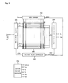
- a plasma display apparatus comprises a plasma display panel 300, a data driver 310 for driving the plasma display panel 300, a scan driver 320, a sustain driver 330, a driving pulse controller 340 and a driving voltage generator 350.
- the plasma display panel 300 comprises a front substrate (not shown) and a rear substrate (not shown), which are adhered together.
- a plurality of scan electrodes Y1 to Yn and a sustain electrode Z are formed in the front substrate in pairs.
- a plurality of address electrodes X1 to Xm crossing the scan electrodes Y1 to Yn and the sustain electrodes Z is formed in the rear substrate.
- the plasma display apparatus includes a phosphor layer (not shown) that partitions discharge spaces formed between the front substrate and the rear substrate. This will be described in detail with reference to FIGS. 4 to 9m later on.
- the data driver 310 applies data to the address electrodes X1 to Xm formed in the plasma display panel 300.
- the data refers to the picture signal data that has been processed by a picture signal processor (not shown) that processes externally input picture signals.
- the data driver 310 samples and latches the data in response to a data timing control signal (CTRX) from the driving pulse controller 340 and supplies an address pulse having an address voltage (Va) to the address electrodes X1 to Xm.
- CTRX data timing control signal
- the scan driver 320 drives the scan electrodes Y1 to Yn formed in the plasma display panel 300.
- the scan driver 320 supplies a set-up pulse and a set-down pulse, which constitute a ramp waveform through a combination of Vs, Vsetup and -Vy that are applied from the driving voltage generator 350, to the scan electrodes Y1 to Yn during a reset period under the control of the driving pulse controller 340.
- the scan driver 320 then sequentially supplies the scan pulses, which are applied from a scan reference voltage (Vsc) to the scan voltage (-Vy), to the scan electrodes Y1 to Yn, respectively, during an address period under the control of the driving pulse controller 340.
- Vsc scan reference voltage
- -Vy scan voltage
- the scan driver 320 then supplies a least one or more sustain pulses for a sustain discharge, which are supplied from a ground (GND) level to a sustain voltage (Vs), to the scan electrodes Y1 to Yn during a sustain period during an address period under the control of the driving pulse controller 340.
- a ground (GND) level to a sustain voltage (Vs)
- Vs sustain voltage
- the sustain driver 330 drives the sustain electrode Z, i.e., a common electrode to the plasma display panel 300.
- the sustain driver 330 supplies a bias voltage (Vzb), which is applied from the driving voltage generator 350, to the scan electrode Z during the address period during an address period under the control of the driving pulse controller 340.
- the sustain driver 330 then supplies at least one or more sustain pulses for a sustain discharge, which are supplied from the ground (GND) level to the sustain voltage (Vs), to the scan electrodes Z during a sustain period under the control of the driving pulse controller 340.
- the driving pulse controller 340 controls the data driver 310, the scan driver 320 and the sustain driver 330 when the plasma display panel 300 is driven. That is, the driving pulse controller 340 generates timing control signals (CTRX, CTRY and CTRZ) for controlling the operation timing and synchronization of the data driver 310, the scan driver 320 and the sustain driver 330 in the reset period, the address period, the sustain period, and transmits the timing control signals (CTRX, CTRY and CTRZ) to the drivers 310, 320 and 330, respectively.
- TCRX, CTRY and CTRZ timing control signals
- the data control signal comprises a sampling clock for sampling data, a latch control signal, and a switching control signal for controlling an on/off time of an energy recovery/supply unit and a driving switch element within the data driver 310.
- the scan control signal comprises a switching control signal for controlling an on/off time of an energy recovery/supply unit and a driving switch element within the scan driver 320.
- the sustain control signal comprises a switching control signal for controlling an on/off time of an energy recovery/supply unit and a driving switch element within the sustain driver 330.
- the driving voltage generator 350 generates driving voltages necessary for the driving pulse controller 340 and the respective drivers 310, 320 and 330 and supplies the generated driving voltages thereto. That is, the driving voltage generator 350 generates the set-up voltage (Vsetup), the scan reference voltage (Vsc), the scan voltage (-Vy), the sustain voltage (Vs), the address voltage (Va) and the bias voltage (Vzb). Control of these driving voltages depends on the composition of the discharge gas or the structure of a discharge cell.
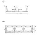
- a front panel 40 and a rear panel 50 are rotated with respect to each other by 90° facilitate understanding of the structure of a discharge cell.
- the front panel 40 comprises a front substrate 41, and scan electrodes Y and sustain electrodes Z formed in the front substrate 41.
- the scan electrode Y comprises a transparent electrode 42Y and a bus electrode 43Y, which has a line width narrower than the line width of the transparent electrode 42Y and is formed at one side of the transparent electrode 42Y.
- the sustain electrode Z comprises a transparent electrode 42Z and a bus electrode 43Z, which has a line width narrower than the line width of the transparent electrode 42Z and is formed at one side of the transparent electrode 42Z.
- the transparent electrodes 42Y, 42Z are formed of ITO and are formed on the front substrate 41.
- the bus electrodes 43Y and 43Z are formed of metal, such as chrome (Cr), and are formed on the transparent electrodes 42Y and 42Z.
- the bus electrodes 43Y and 43Z serve to function to reduce the voltage drop incurred by the transparent electrodes 42Y and 42Z with high resistance.
- a light-shielding layer 58 corresponding to a width of the bus electrode 43Y is formed between the transparent electrode 42Y and the bus electrode 43Y.
- a light-shielding layer 58 corresponding to a width of the bus electrode 43Z is also formed between the transparent electrode 42Z and the bus electrode 43Z.
- the light-shielding layer 58 is formed of a black material and functions to prevent light, which is externally incident on the bus electrodes 43Y and 43Z, from being radiated again outwardly. In other words, the light-shielding layer 58 prevents externally incident light from being emitted outwardly by absorbing the incident light, thus preventing a decrease in the contrast of a plasma display panel.
- a front dielectric layer 44 and a protection layer 46 are laminated on the bottom surface of the front substrate 41 in which the scan electrodes Y and the sustain electrodes Z are formed in parallel. Wall charges generated during the discharge of plasma are accumulated on the front dielectric layer 44.
- the protection layer 46 to prevent damage to the front dielectric layer 44, which can be incurred by sputtering generated during the discharge of plasma, and enhance emission efficiency of the secondary electrons.
- the protection layer 46 is usually formed of magnesium oxide (MgO).
- Black layers 45 are formed at the interfaces of the discharge cells.
- the black layers 45 absorb external incident light and light that is radiated from the discharge cells to the outside, thus preventing a decrease in the contrast of the plasma display panel.
- the rear panel 50 comprises a rear substrate 48, address electrodes X1 and X2 formed on the rear substrate 48, and a rear dielectric layer 52 formed on the rear substrate 48 and the address electrodes X1 and X2, and barrier ribs 54a and 54b.
- On surfaces of the rear dielectric layer 52 and the barrier ribs 54a and 54b are formed two or more phosphor layers 56a and 56b whose excited wavelengths are different from each other.
- the address electrodes X1 and X2 cross the scan electrode Y and the sustain electrodes Z.
- the barrier ribs 54a and 54b are formed in stripe or lattice form, and to prevent ultraviolet rays and/or a visible ray, which are generated by a discharge, from leaking to adjacent discharge cells.
- the barrier ribs 54a and 54b support discharge spaces when the front panel 40 and the rear panel 50 are adhered together.
- the phosphor layers 56a and 56b are formed on the barrier ribs 54a and 54b and the rear dielectric layer 52 and are excited by ultraviolet rays, which are generated during the discharge of plasma, to generate any one of R (red), G (green) or B (blue) visible rays.
- the phosphor layers 56a and 56b partition discharge spaces between the front substrate 41 and the rear substrate 48, which are combined together with a predetermined distance therebetween. In the present embodiment, two discharge spaces are partitioned.
- the first barrier rib 54a is formed between two or more discharge spaces.
- the second barrier rib 54b is adjacent to the first barrier rib 54a.
- Each of the two discharge spaces comprises the address electrodes X1 and X2.
- the rear dielectric layer 52 covering the address electrodes X1 and X2 is formed in each discharge space.
- the phosphor layers 56a and 56b being comprised of different materials, i.e., excited wavelengths are different from each other, are formed in discharge spaces adjacent to each other, respectively.
- the phosphor layers 56a and 56b whose excited wavelengths are at least two or more are formed between the first and second barrier ribs 54a and 54b, the phosphor layers 56a and 56b have a step between a region to which the discharge spaces belong and a region that partitions the discharge spaces.
- the thickness (B) of a portion of the phosphor layer 56a that partitions the discharge spaces is more than the thickness (A) of a portion of the phosphor layer 56a belonging to the discharge space, so that the discharge spaces are partitioned.
- the term "phosphor layer" partitioning discharge spaces refers to a phosphor layer serving as a kind of a barrier rib that partitions R, G and B discharge cells only with the phosphor layer itself without the structure of barrier ribs.
- barrier ribs are not formed at the interfaces of the phosphor layers 56a and 56b partitioning the discharge spaces in FIG. 4 , a phosphor layer formed on an opposite side is formed on the barrier ribs 54a and 54b. It is therefore possible to secure a sufficient discharge space even without reducing the size of a discharge cell since a portion where conventional barrier ribs are formed serves as a reserved space. Therefore, when the pitch in a plasma display panel is the same as that of a discharge cell in the known plasma display panel, the number of discharge cells integrated on the plasma display panel is increased.
- the maximum thickness of the phosphor layers 56a and 56b belonging to a region that partitions discharge spaces is from more than 50% to less than 100% of the maximum thickness of the barrier ribs 54a and 54b. If the maximum thickness is 50% or less, respective discharge spaces are not clearly partitioned, which may abruptly increase cross talk toward adjacent discharge cells. If the maximum thickness is 100% or higher, this may lower the convenience of a manufacturing process and degrade an exhaust characteristic of impurities. In consideration of such cross talk between discharge cells, the maximum thickness of the phosphor layers 56a and 56b that partition discharge spaces should not be less than 80% with respect to the maximum thickness of the barrier ribs 54a and 54b. To improve an exhaust characteristic while reducing cross talk, the center of a top surface of the phosphor layers 56a and 56b that partition the discharge space groove.
- a width of the phosphor layers 56a and 56b that partition discharge spaces is wider than the width of the phosphor layers formed on the barrier ribs 54a, 54b.
- the phosphor layers 56a and 56b that partition the discharge spaces can comprise a barrier rib material to secure rigidity.
- the barrier rib material present in a material forming the phosphor layers 56a and 56b should be 50% or less of a total percentage of the material forming the phosphor layers 56a and 56b.
- a glass ceramics material can be used as the barrier rib material.
- the discharge space 60 partitioned by the phosphor layers 56a and 56b between the two barrier ribs 54a and 54b is two in number.
- the present invention can be applied to a case where the number of the discharge space 60 partitioned by the phosphor layers 56a and 56b between both barrier ribs 54a and 54b is 2 or higher.
- one address electrode is disposed in each of the discharge spaces 60.
- FIG. 5 illustrates a modified structure of a plasma display panel.
- widths of the discharge spaces partitioned by phosphor layers are different from each other.
- the phosphor layers whose materials, i.e., excited wavelengths are different from each other are formed in adjacent discharge spaces.
- Each of the phosphor layers becomes one of R, G or B phosphor layers. Since the R, G or B phosphor layers have different saturation characteristics, they have different brightness characteristics although the number of sustain pulses applied to respective discharge spaces is the same. Therefore, in the present embodiment, the widths of the discharge spaces are formed to be different from each other by taking the brightness characteristics of the phosphor layers into consideration.
- a width (b) of a discharge space of a phosphor layer 56b with a low brightness characteristic, of the phosphor layers 56a and 56b of the discharge spaces 60 and 61 is wider than a width (a) of a discharge space of the phosphor layer 56a with a high brightness characteristic. Therefore, when forming phosphor layers, discharge spaces can be partitioned and white balance can also be controlled.
- white balance can be controlled using not only discharge spaces, but also regions that partition the discharge spaces.
- At least two or more discharge spaces are partitioned by phosphor layers.
- regions partitioning the discharge spaces are formed using one kind of a material
- mixed light is generated by the material of the regions that partitions the discharge spaces when discharge light is generated in an opposite discharge space having a different material unlike discharge spaces having the same material.
- phosphor layers are formed of two different materials in regions that partition discharge spaces.
- the material may be the same as that of a phosphor layer of each of neighboring discharge spaces with respect to the regions partitioning the discharge spaces.
- the widths of the phosphor layers formed using two kinds of materials are different from each other in regions that partition discharge spaces. That is, the widths of the regions that partition the discharge spaces are formed to be different from each other in consideration of a brightness characteristic of regions that partition discharge spaces formed using different materials.
- a width (d) of a region that partitions the discharge space of the phosphor layer 56b with a high brightness characteristic, of the phosphor layers 56a and 56b of the discharge spaces 60 and 61 is wider than a width (c) of the region that partitions the discharge space of the phosphor layer 56a with a low brightness characteristic.
- a pitch of a discharge cell with a high brightness characteristic becomes lower than that of a discharge cell with a low brightness characteristic.
- black layers are formed on regions that partition discharge spaces of phosphor layers.
- the black layers are formed on the front panel.
- black layers 70 and 71 are formed on barrier ribs 54a and 54b, or a black layer 72 is formed on a region that partitions a discharge space of the phosphor layers 56a and 56b.
- the black layer 72 is formed in the region that partitions the discharge space of the phosphor layers 56a and 56b, a mixed color between adjacent discharge cells will be prevented and a manufacturing process of the black layers can be facilitated.
- the widths of the black layers 72 which are formed in regions that partition the discharge spaces, to be different from each other, the degree of shielded light emitted from a top surface of a region that partitions discharge spaces. For instance, by controlling widths of black layers formed to be different depending on materials of R, G and B phosphor layers, the white balance of a plasma display panel will be controlled.
- FIG. 7 shows that the black layers 72 are formed in a wider area on the phosphor layer 56a with a high brightness characteristic.
- a front panel 60 and a rear substrate 70 are rotated with respect to each other by 90° to facilitate understanding of the structure of the plasma display panel.
- the bundle of R, G and B discharge cells form the least unit that can display a desired color.
- the least unit that can display a color will be referred to as "R, G and B unit discharge cell.”
- a barrier rib is formed for every unit discharge cell.
- R, G and B unit discharge cells can be formed between a first barrier rib 74a and a second barrier ribs 74b, and the R, G and B unit discharge cells are partitioned with a step being given to phosphor layers.
- the barrier ribs 74a and 74b will be thicker than the phosphor layers. Since color interference between the R, G and B unit discharge cells is reduced by the barrier ribs formed between the R, G and B unit discharge cells, the picture quality of images that are implemented can be further improved. In addition, by using the spaces of the conventional barrier ribs that had been formed for every R, G and B discharge cells as surplus spaces, images with high resolution can be implemented.
- Embodiments are not restricted to plasma display panels having the structure of the phosphor layers that partition the discharge space, which has been described with reference to FIGS. 4 to 8 . That is, although a barrier rib can be formed every R, G and B unit discharge cells, a barrier rib can be formed for every two or more R, G and B unit discharge cells.
- Barrier ribs may not be formed within a valid display region on which images are displayed, but discharge cells can be partitioned by only phosphor layers.
- a phosphor layer located at the outermost of the valid display region can be preferably formed using a barrier rib to support an upper substrate.
- Embodiments may include various structures of discharge cell, for example, a strip type, a well type, a fish bone type, a honeycomb type and a waffle type.
- discharge cells are partitioned by four upper, lower, right and left barrier ribs.
- a phosphor layer serving as a barrier rib can be formed at any one of upper, lower, right and left places.
- the number of phosphor layers can also range from 1 to 4.
- the phosphor layers intersect two barrier ribs.
- the phosphor layers can intersect one barrier rib while crossing each other and cross two barrier ribs.
- a width and/or thickness of the phosphor layers that intersect each other can be substantially the same or different from each other.
- the numerical value of the thickness of phosphor layers, a material of phosphor layers, a width of phosphor layer, formation of black layers and the like can be applied in the same manner as the aforementioned embodiment.
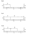
- FIGS. 9a to 9m illustrate a manufacturing process of a plasma display panel.
- address electrodes X1, X2 and X3 are formed on a rear substrate 48 by a photolithography process, etc.
- Address electrode layers are deposited as a thin film on the rear substrate 48 by a sputtering or spin and spinless method.
- a photoresist is then coated on the entire deposited thin film.
- a screen mask having a shape desired by a user is placed on the coated photoresist.
- the photoresist other than the masked portions is exposed using ultraviolet rays (UV).
- UV ultraviolet rays
- the exposed photoresist is developed using a developer.
- An etch process is then performed to form the address electrodes X1, X2 and X3.
- a dielectric material is blanket printed on the rear substrate 48 having the address electrodes X1, X2 and X3 formed thereon, forming a dielectric layer 52.
- barrier ribs 54a and 54b are formed on the dielectric layer 52 using one of molding, sandblasting and photolithography methods.
- a mold having an engraving shape of barrier ribs which will be formed on a green sheet, is pressurized to form the barrier ribs 54a and 54b.
- a dry film i.e., a photosensitive material
- paste for barrier ribs which is deposited on the entire surface.
- a mask having the same shape as that of the barrier ribs is disposed.
- the dry film at a portion that has not been masked is then exposed to ultraviolet rays.
- the exposed dry film is then developed using a developer. Thereafter, the paste for barrier ribs at the portion in which the dry film has been developed is physically removed by spraying particles, thereby completing the barrier ribs 54a and 54b.
- a photoresist i.e., a photosensitive material
- paste for barrier ribs which is deposited on the entire surface.
- a mask that has the same shape as that of the barrier ribs is placed.
- the photoresist that has not been masked is then exposed by irradiating UV onto a top surface of the mask.
- the exposed photoresist is then developed using a developer. Thereafter, the paste for barrier ribs at a portion in which the photoresist has been developed is removed through chemical reaction of an etching process, thereby completing the barrier ribs 54a and 54b.
- First to third phosphor layers are formed between these barrier ribs 54a and 54b through subsequent processes of FIGS. 9d to 9h .
- an inkjet spray method, a squeezing method or the like is employed.
- a first phosphor paste is coated on the entire surface of the dielectric layer 52 to form a first phosphor layer 56a.
- portions other than the first phosphor layer 56a formed on the dielectric layer 52 of the first address electrode X1 are removed by a photolithography process.
- a second phosphor paste is coated on regions other than the first phosphor layer 56a, thus forming a second phosphor layer 56b between the first phosphor layer 56a and the barrier ribs 54b.
- portions other than the first and the second phosphor layers 56a and 56b formed on the dielectric layer 52 of the first and second address electrodes X1 and X2 are removed.
- a third phosphor paste is coated to form a third phosphor layer 56c on the dielectric layer 52 of the third address electrode X3.
- a discharge space region and a region for partitioning a discharge space are formed as follows.
- a photoresist 64 is coated on the entire surface of the first to third phosphor layers 56a, 56b and 56c.
- the photoresist 64 at the interfaces of the first to third phosphor layers 56a, 56b and 56c, i.e., portions other than a region that partitions a discharge space is exposed using UV.
- the photoresists 64 are developed using a developer.
- an etch process is performed to form discharge spaces 60, and the first to third phosphor layers 56a, 56b and 56c that partition the discharge spaces.
- the photoresists 64 are stripped using a strip solution, completing a rear panel. Thereafter, a process of forming black layers (not shown) on a region that partitions the discharge spaces of the barrier ribs 54a and 54b or the phosphor layers 56a, 56b and 56c may be further included.
- the photolithography process of forming the first to third phosphor layers 56a, 56b and 56c and the photolithography process of forming the discharge spaces, of the manufacturing process of the plasma display panel can employ a method using other processes for the same object, such as a sandblast process or a process of laminating, exposing developing and etching a dry film. That is, the plasma display panel is not restricted to the manufacturing process described.
Landscapes
- Physics & Mathematics (AREA)
- Engineering & Computer Science (AREA)
- Plasma & Fusion (AREA)
- Gas-Filled Discharge Tubes (AREA)
Claims (17)
- Panneau d'affichage à plasma, comprenant: un substrat avant (41) et un substrat arrière (48) qui sont combinés, avec une distance prédéterminée entre eux; caractérisé en ce que:deux ou plusieurs couches de phosphore (56a; 56b; 56c) sont positionnées entre des nervures de barrières adjacentes (54a; 54b), et séparent deux ou plusieurs cellules de décharge entre le substrat avant (41) et le substrat arrière (48),où une lumière de différentes couleurs est produite lorsque les deux couches de phosphore précitées ou plus (56a; 56b; 56c) sont excitées par la décharge.
- Panneau d'affichage à plasma selon la revendication 1, où deux ou plusieurs cellules de décharge sont séparées par deux nervures de barrière (54a;54b) sur lesquelles les couches de phosphore (56a;56b;56c) sont appliquées.
- Panneau d'affichage à plasma selon la revendication 1 ou 2, où une ou plusieurs couches de phosphore (56a;56b;56c) se croisent avec d'autres couches de phosphore qui séparent les cellules de décharge dans une direction différente d'une direction dans laquelle une ou plusieurs premières couches de phosphore (56a;56b;56c) sont formés, ou nervures de barrière.
- Panneau d'affichage à plasma selon l'une des revendications précédentes, où l'épaisseur (B) d'une portion de la couche de phosphore (56a;56b;56c) qui divise les espaces de décharge est plus grande que l'épaisseur (A) d'une portion de la couche de phosphore (56a;56b;56c) de la cellule de décharge.
- Panneau d'affichage à plasma selon la revendication 1, où l'épaisseur des couches de phosphore (56a;56b;56c) s'étend depuis plus que 80% et à moins que 100% de l'épaisseur des nervures de barrière (54a;54b) formées sur un substrat arrière (48).
- Panneau d'affichage à plasma selon la revendication 1, où les couches de phosphore (56a;56b;56c) comprennent des matériaux différents.
- Panneau d'affichage à plasma selon la revendication 1, où les couches de phosphore (56a;56b;56c) produisent des lumières de longueurs d'ondes différentes.
- Panneau d'affichage à plasma selon la revendication 1, où des pas des cellules de décharge divisés par les couches de phosphore (56a;56b;56c) diffèrent les uns des autres.
- Panneau d'affichage à plasma selon la revendication 8, où le pas d'une cellule de décharge bleue ou d'une cellule de décharge verte est plus grand que le pas d'une cellule de décharge rouge.
- Panneau d'affichage à plasma selon la revendication 1, où les couches de phosphore (56a;56b;56c) ont des largeurs différentes dans la région où les espaces de décharge sont divisés.
- Panneau d'affichage à plasma selon la revendication 10, où la largeur d'une région de cellules de décharge bleue ou d'une région de cellule de décharge verte est plus petite que la largeur d'une région de cellule de décharge rouge.
- Panneau d'affichage à plasma selon la revendication 3, où les couches de phosphore (56a;56b;56c) comprennent un matériau de nervure de barrière.
- Panneau d'affichage à plasma selon la revendication 12, où le matériau de nervure de barrière présent dans un matériau formant les couches de phosphore (56a;56b;56c) représente 50% ou moins d'un pourcentage total du matériau formant les couches de phosphore (56a;56b;56c).
- Panneau d'affichage à plasma selon la revendication 1, où les couches de phosphore (56a;56b;56c) ont des couches noires (70;71) formées à leur extrémité supérieure.
- Panneau d'affichage à plasma selon la revendication 14, où les largeurs des couches noires (70;71) formées dans des régions où les espaces de décharge sont divisés, sont différentes les unes des autres.
- Panneau d'affichage à plasma selon la revendication 1, où le substrat avant (41) comprend:des électrodes d'exploration (Y) et des électrodes de soutient (Z), qui sont espacées les unes des autres à des distances prédéterminées pour chaque cellule de décharge et sont agencées en parallèle;une ou plusieurs couches diélectriques (44) couvrant les électrodes d'exploration (Y) et les électrodes de soutient (Z); etun recouvrement de couche de protection (46) pour protéger la couche diélectrique (44).
- Panneau d'affichage à plasma selon la revendication 1, où le substrat arrière (48) comprend:des électrodes d'adresse (X) agencées dans chaque cellule de décharge en parallèle, et une couche diélectrique (44) couvrant les électrodes d'adresse (X).
Applications Claiming Priority (1)
| Application Number | Priority Date | Filing Date | Title |
|---|---|---|---|
| KR1020040082241A KR20060033244A (ko) | 2004-10-14 | 2004-10-14 | 플라즈마 디스플레이 패널 |
Publications (3)
| Publication Number | Publication Date |
|---|---|
| EP1648012A2 EP1648012A2 (fr) | 2006-04-19 |
| EP1648012A3 EP1648012A3 (fr) | 2006-08-02 |
| EP1648012B1 true EP1648012B1 (fr) | 2008-09-24 |
Family
ID=35562401
Family Applications (1)
| Application Number | Title | Priority Date | Filing Date |
|---|---|---|---|
| EP05256388A Expired - Lifetime EP1648012B1 (fr) | 2004-10-14 | 2005-10-13 | Panneau d'affichage à plasma |
Country Status (5)
| Country | Link |
|---|---|
| US (1) | US20060097647A1 (fr) |
| EP (1) | EP1648012B1 (fr) |
| KR (1) | KR20060033244A (fr) |
| CN (1) | CN1761022A (fr) |
| DE (1) | DE602005009905D1 (fr) |
Family Cites Families (8)
| Publication number | Priority date | Publication date | Assignee | Title |
|---|---|---|---|---|
| US5136207A (en) * | 1989-02-10 | 1992-08-04 | Dai Nippon Insatsu Kabushiki Kaisha | Plasma display panel having cell barriers of phosphor containing material |
| US6787995B1 (en) * | 1992-01-28 | 2004-09-07 | Fujitsu Limited | Full color surface discharge type plasma display device |
| EP0884754B1 (fr) * | 1996-12-17 | 2006-04-12 | Toray Industries, Inc. | Procede de fabrication d'ecran a plasma et dispositif correspondant |
| JPH11306996A (ja) * | 1998-02-23 | 1999-11-05 | Mitsubishi Electric Corp | 面放電型プラズマディスプレイ装置、面放電型プラズマディスプレイパネル及び面放電型プラズマディスプレイパネル用基板 |
| TW423006B (en) * | 1998-03-31 | 2001-02-21 | Toshiba Corp | Discharge type flat display device |
| JP3909506B2 (ja) * | 1998-08-19 | 2007-04-25 | 株式会社日立プラズマパテントライセンシング | プラズマディスプレイパネル及びその製造方法 |
| JP3864204B2 (ja) * | 1999-02-19 | 2006-12-27 | 株式会社日立プラズマパテントライセンシング | プラズマディスプレイパネル |
| US7118687B2 (en) * | 2002-07-24 | 2006-10-10 | Konica Corporation | Phosphor, method for producing phosphor and its precursor, and display device |
-
2004
- 2004-10-14 KR KR1020040082241A patent/KR20060033244A/ko not_active Withdrawn
-
2005
- 2005-10-13 DE DE602005009905T patent/DE602005009905D1/de not_active Expired - Lifetime
- 2005-10-13 US US11/248,586 patent/US20060097647A1/en not_active Abandoned
- 2005-10-13 EP EP05256388A patent/EP1648012B1/fr not_active Expired - Lifetime
- 2005-10-14 CN CNA2005101137479A patent/CN1761022A/zh active Pending
Also Published As
| Publication number | Publication date |
|---|---|
| EP1648012A3 (fr) | 2006-08-02 |
| KR20060033244A (ko) | 2006-04-19 |
| US20060097647A1 (en) | 2006-05-11 |
| EP1648012A2 (fr) | 2006-04-19 |
| DE602005009905D1 (de) | 2008-11-06 |
| CN1761022A (zh) | 2006-04-19 |
Similar Documents
| Publication | Publication Date | Title |
|---|---|---|
| US6580227B2 (en) | Plasma display panel, manufacturing method thereof, and plasma display | |
| US20050218807A1 (en) | Plasma display panel and manufacture method thereof | |
| EP1648012B1 (fr) | Panneau d'affichage à plasma | |
| JP4670990B2 (ja) | プラズマディスプレイパネル | |
| JP2005249949A (ja) | プラズマディスプレイパネルの駆動方法 | |
| KR100692095B1 (ko) | 플라즈마 디스플레이 패널의 격벽, 플라즈마 디스플레이 패널 및 그의 제조방법 | |
| US20060214884A1 (en) | Plasma display panel driving method and plasma display apparatus | |
| US8330367B2 (en) | Plasma display panel | |
| US7377831B2 (en) | Plasma display panel and method of manufacturing the same | |
| JP4109144B2 (ja) | プラズマディスプレイパネル | |
| US7157855B2 (en) | Plasma display panel | |
| KR100831008B1 (ko) | 플라즈마 디스플레이 패널 및 그 제조방법 | |
| US20100127623A1 (en) | Plasma display panel | |
| KR100692063B1 (ko) | 플라즈마 디스플레이 패널 전면기판용 그린시트 및 그 제조방법 | |
| JP4540090B2 (ja) | プラズマディスプレイパネルの駆動方法 | |
| KR100484644B1 (ko) | 더미 전극을 갖는 플라즈마 디스플레이 패널 | |
| KR20010048519A (ko) | 개선된 플라즈마 디스플레이 패널 | |
| KR100708653B1 (ko) | 플라즈마 디스플레이 패널 | |
| KR20060109010A (ko) | 플라즈마 디스플레이 패널 및 그의 제조방법 | |
| JP2009252622A (ja) | プラズマディスプレイパネル | |
| KR20060029094A (ko) | 플라즈마 디스플레이 패널 | |
| KR20060029093A (ko) | 플라즈마 디스플레이 패널 | |
| JP2003076318A (ja) | プラズマディスプレイパネルの駆動方法 | |
| KR20060072818A (ko) | 플라즈마 디스플레이 패널의 제조방법 | |
| JP2007134264A (ja) | プラズマディスプレイパネル |
Legal Events
| Date | Code | Title | Description |
|---|---|---|---|
| PUAI | Public reference made under article 153(3) epc to a published international application that has entered the european phase |
Free format text: ORIGINAL CODE: 0009012 |
|
| 17P | Request for examination filed |
Effective date: 20060124 |
|
| AK | Designated contracting states |
Kind code of ref document: A2 Designated state(s): AT BE BG CH CY CZ DE DK EE ES FI FR GB GR HU IE IS IT LI LT LU LV MC NL PL PT RO SE SI SK TR |
|
| AX | Request for extension of the european patent |
Extension state: AL BA HR MK YU |
|
| PUAL | Search report despatched |
Free format text: ORIGINAL CODE: 0009013 |
|
| AK | Designated contracting states |
Kind code of ref document: A3 Designated state(s): AT BE BG CH CY CZ DE DK EE ES FI FR GB GR HU IE IS IT LI LT LU LV MC NL PL PT RO SE SI SK TR |
|
| AX | Request for extension of the european patent |
Extension state: AL BA HR MK YU |
|
| 17Q | First examination report despatched |
Effective date: 20070213 |
|
| AKX | Designation fees paid |
Designated state(s): DE FR GB NL |
|
| GRAP | Despatch of communication of intention to grant a patent |
Free format text: ORIGINAL CODE: EPIDOSNIGR1 |
|
| GRAS | Grant fee paid |
Free format text: ORIGINAL CODE: EPIDOSNIGR3 |
|
| GRAA | (expected) grant |
Free format text: ORIGINAL CODE: 0009210 |
|
| AK | Designated contracting states |
Kind code of ref document: B1 Designated state(s): DE FR GB NL |
|
| REG | Reference to a national code |
Ref country code: GB Ref legal event code: FG4D |
|
| REF | Corresponds to: |
Ref document number: 602005009905 Country of ref document: DE Date of ref document: 20081106 Kind code of ref document: P |
|
| PLBE | No opposition filed within time limit |
Free format text: ORIGINAL CODE: 0009261 |
|
| STAA | Information on the status of an ep patent application or granted ep patent |
Free format text: STATUS: NO OPPOSITION FILED WITHIN TIME LIMIT |
|
| 26N | No opposition filed |
Effective date: 20090625 |
|
| PGFP | Annual fee paid to national office [announced via postgrant information from national office to epo] |
Ref country code: NL Payment date: 20130911 Year of fee payment: 9 |
|
| PGFP | Annual fee paid to national office [announced via postgrant information from national office to epo] |
Ref country code: GB Payment date: 20130911 Year of fee payment: 9 Ref country code: FR Payment date: 20130912 Year of fee payment: 9 |
|
| PGFP | Annual fee paid to national office [announced via postgrant information from national office to epo] |
Ref country code: DE Payment date: 20130912 Year of fee payment: 9 |
|
| REG | Reference to a national code |
Ref country code: DE Ref legal event code: R119 Ref document number: 602005009905 Country of ref document: DE |
|
| REG | Reference to a national code |
Ref country code: NL Ref legal event code: V1 Effective date: 20150501 |
|
| GBPC | Gb: european patent ceased through non-payment of renewal fee |
Effective date: 20141013 |
|
| PG25 | Lapsed in a contracting state [announced via postgrant information from national office to epo] |
Ref country code: GB Free format text: LAPSE BECAUSE OF NON-PAYMENT OF DUE FEES Effective date: 20141013 Ref country code: DE Free format text: LAPSE BECAUSE OF NON-PAYMENT OF DUE FEES Effective date: 20150501 |
|
| REG | Reference to a national code |
Ref country code: FR Ref legal event code: ST Effective date: 20150630 |
|
| PG25 | Lapsed in a contracting state [announced via postgrant information from national office to epo] |
Ref country code: FR Free format text: LAPSE BECAUSE OF NON-PAYMENT OF DUE FEES Effective date: 20141031 Ref country code: NL Free format text: LAPSE BECAUSE OF NON-PAYMENT OF DUE FEES Effective date: 20150501 |