EP1648029A2 - Dispositif de contact pour modules semiconducteur de puissance et cellules discoides semiconductrices - Google Patents
Dispositif de contact pour modules semiconducteur de puissance et cellules discoides semiconductrices Download PDFInfo
- Publication number
- EP1648029A2 EP1648029A2 EP05017563A EP05017563A EP1648029A2 EP 1648029 A2 EP1648029 A2 EP 1648029A2 EP 05017563 A EP05017563 A EP 05017563A EP 05017563 A EP05017563 A EP 05017563A EP 1648029 A2 EP1648029 A2 EP 1648029A2
- Authority
- EP
- European Patent Office
- Prior art keywords
- contact
- power semiconductor
- spring
- connection
- contact device
- Prior art date
- Legal status (The legal status is an assumption and is not a legal conclusion. Google has not performed a legal analysis and makes no representation as to the accuracy of the status listed.)
- Granted
Links
Images


Classifications
-
- H—ELECTRICITY
- H10—SEMICONDUCTOR DEVICES; ELECTRIC SOLID-STATE DEVICES NOT OTHERWISE PROVIDED FOR
- H10W—GENERIC PACKAGES, INTERCONNECTIONS, CONNECTORS OR OTHER CONSTRUCTIONAL DETAILS OF DEVICES COVERED BY CLASS H10
- H10W72/00—Interconnections or connectors in packages
Definitions
- a contact device for the control connection of power semiconductor components in disk cells and power semiconductor modules is described.
- Such contact devices are part of disc cells as they are known by way of example from Heumann, "Basics of Power Electronics", Teubner Verlag, 6th edition, ISBN 3-519-06110-4, page 37 and preferably pressure-contacted power semiconductor modules as exemplified in DE 196 51 632 A1 are known.
- Pressure-contacted power semiconductor modules such as those according to DE 196 51 632 A1 are suitable for very high power requirements in terms of current carrying capacity and reliability. Therefore, the control connection plays an equally important role here as the power connections.
- Pressure contact connections of the power terminals are well known from the production of semiconductor modules as a connection technique and proven many times. In contrast, there are a variety of variants with different levels of manufacturing complexity and not directly associated with different levels of reliability for the contact connection of control terminals.
- the invention has for its object to present a contact device of the control terminal of power semiconductor devices in disc cells and power semiconductor modules, which is universally applicable, ensures a permanently secure electrical contact and a simple assembly is accessible.
- the basic idea of the invention is based on a power semiconductor module, preferably in pressure contact with one or more power semiconductor components or a disk cell.
- a disk cell typically only one power semiconductor device is arranged, but there are special forms with a plurality of power semiconductor devices in a housing.
- the invention relates to power semiconductor modules or disk cells with at least one controlled power semiconductor device, such as a thyristor or a transistor. These have a control terminal, which is acted upon from outside the power semiconductor module or the disk cell with a control signal.
- a controlled power semiconductor device such as a thyristor or a transistor.
- the semiconductor devices in power semiconductor modules and disc cells are connected on both sides with a flat metal body, the coefficient of thermal expansion between the coefficient of thermal expansion of the semiconductor device and the coefficient of thermal expansion of a subsequent contact means of the power terminals is to reduce the thermal stress for the semiconductor device.
- the connection of the semiconductor component with the flat metal bodies which preferably consist of molybdenum, can be realized by different methods, for example by soldering, gluing or pressure contacting of the two partners.
- the sheet metal body typically has a thickness of the order of a few tenths to a few millimeters.
- the contact device according to the invention for contacting the control terminal of the at least one power semiconductor component is assigned to the main surface and the control connection carrying main surface a molded body, for example, the above-mentioned sheet metal body.
- This shaped body has in the area above the control terminal on a recess and this recess in turn has an abutment.
- the contact device itself consists of a contact spring with a pin-like extension at that end of the spring, which contacts the control terminal. Furthermore, it has a connection formed directly or via a metal mold part with a connection cable to the external connection at the other end of the spring.
- the contact spring and the optional metal molded part are arranged in an insulating sleeve, said insulating sleeve having at least one locking lug which forms a snap-locking connection together with the abutment of the molded body.
- Fig. 1 shows an embodiment of a disc cell according to the prior art.
- FIG. 2 shows a section through an embodiment of a pressure-contacted power semiconductor module according to the prior art.
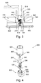
- FIG 3 shows a contact device according to the invention in a power semiconductor module.
- FIG. 4 shows a three-dimensional exploded view of a contact device according to the invention.
- FIG. 5 shows a three-dimensional exploded view of a power semiconductor module with a contact device according to the invention.
- Fig. 1 shows a partial section through a disc cell (950) according to the prior art.
- This has an insulating body (954), preferably made of ceramic.
- This Isolierstoff Ari (954) forms the housing of the disc cell (950), their upper and lower cover (956, 952) are formed as metal moldings.
- a power semiconductor device (600) is arranged inside the disc cell (950).
- the one metal shaped body (956) has a recess (958).
- the gate contact is arranged.
- This is designed as a resilient wire element (962) with an insulating sheath. The insulation covers only the part of the Wire element (962), which can come into contact with the metal moldings (956).
- the first end of the wire element (962) is arranged in a recess of the insulating material body (956) provided with a metal sleeve (964) and thus electrically conductively connected thereto.
- the second end (960) of the wire element (962) rests on the gate of the power semiconductor device (600).
- the arrangement in the metal sleeve (964) and the shape of the wire element (962) results in a spring action with an introduction of force to the second end (960) of the wire element (962) in the direction of the power semiconductor component (600).
- a disadvantage of this embodiment of the disc cell (950) is that the metal shaped body (956) must have a radially outwardly running recess (958) for receiving the wire element (962). This is not cost effective to produce, nor is the assembly of the contact device can be automated.
- FIG. 2 shows a section through an embodiment of a pressure-contacted power semiconductor module (900) according to the prior art. Shown here is a metallic base plate (902), a plastic housing (908) and a plastic lid (910). On the base plate (902), a first metal shaped body (904) is subsequently arranged on an insulating layer, on which is arranged a power semiconductor component (600) and via this a second metallic molded body (908). This second metallic molded body (908) is pressurized by means of a pressure contact device (906) and thus presses the semiconductor component (600) against the first molded body (904) and this against the base plate (902). Thus, a secure electrical contact of the semiconductor device (600) to the two moldings (904, 908) and in addition a thermal contact with the base plate (902) is ensured. The two metallic moldings (904, 908) thus serve to make contact with the main connections.
- the control terminal (610) of the power semiconductor component (600) is contacted by means of a contact device.
- This contact device consists of a metallic wire element (914) which is fixed in a holding device (912) of the housing. Starting from this holding device (912), an electrically insulated wire connection (916) to an external connection is provided.
- the second metallic molded body (908) has a recess (920), in the course of which the wire element (914) is arranged and contacts the control terminal (610) there.
- the wire element (914) and its holding device (912) are designed such that the wire element (914) builds a spring force directed toward the power semiconductor device (600).
- the control terminal of the power semiconductor module (900) is designed in pressure contact technology.
- a disadvantage of this configuration of the contact device is that the pressure introduction to the power semiconductor component (600) does not occur radially symmetrically through the recess (920) in the second molded body (908).
- Another disadvantage is that the contact devices are designed differently for different power classes of the power semiconductor module (900) and, consequently, different diameters of the power semiconductor component (600). The installation effort of the contact device is also here contrary to a cost-effective production.
- a further disadvantage of the configurations of the contact devices for disc cells according to FIG. 1 and power semiconductor modules according to FIG. 2 is that the spring arm thus extends the lateral extent between the holder (964, 912) and the contact point to the control terminal (610) of the power semiconductor component (600). is very big. Under this embodiment of the resilient wire element (962, 914) suffers the contact reliability, since the homogeneity of the spring force on the production of a variety of disc cells or power semiconductor modules is given only with considerable effort.
- FIG. 3 shows a contact device according to the invention in a power semiconductor module.
- a power semiconductor device (600) with a control terminal (610) arranged centrally on the first main surface and a first and a second power connection (620) arranged on the two opposite major surfaces of the power semiconductor device (600).
- a metallic molded body (700) formed from the sandwich of two partial molded bodies is arranged. This shaped body (700) has a round central recess (710) which has an edge (720).
- the contact device itself consists of an insulating sleeve (300), consisting of a thermoplastic or preferably duroplastic plastic, a spring element (100) and a plug formed as a metal molding (200).
- the plastic sleeve (300) is used for electrical isolation of the control signal from the power connection, which is formed by the metallic molded body (700).
- the plastic sleeve (300) has two Latching lugs (360) on. These locking lugs (360) form with the serving as abutment edge (720) of the metallic molding (700) a snap-locking connection.
- a simple mounting of the contact device in the metallic molded body (700) is possible.
- the plastic sleeve (300) designed as a barrel spring contact spring (100) is arranged inside the plastic sleeve (300) designed as a barrel spring contact spring (100) is arranged. This has on its side facing the power semiconductor component (600) side facing a centrally arranged to the spring axis pin-like extension (110) with differently shaped end. This can be exemplified dull, convex or arc, as shown, be formed.
- the extension (110) penetrates the plastic sleeve (300), wherein it is formed in such a way that the spring element (100) is secured against falling out in the direction of the control connection (610).
- the extension (110) serves to make contact with the control connection (610) of the power semiconductor component (600).
- the resilient portion of the contact spring (100) is used over the life of the disc cell or the power semiconductor module constant pressure introduction and thus secure contacting of the control terminal (610).
- the metal mold part (200) which is likewise arranged in the interior of the plastic sleeve (300), serves for electrically connecting the contact spring (100) to the external control connection of the pane cell or power semiconductor component.
- the metal mold part (200) on a first pin (210) which serves to guide the metal molding (200) and extends into the inner region of the contact spring (100).
- two further pins (230) are arranged perpendicular to the first pin (210), which form a stop for the contact spring (100) and thus serve to build up pressure.
- the metal shaped part (200) For connection to a connecting cable (500), which has a plug sleeve (510), the metal shaped part (200) has a second pin (220), which is designed as a plug. Thus, the connection to an external terminal is formed.
- the contact device such that the plastic sleeve (300) is formed such that it itself has an abutment for the spring element and the power semiconductor device facing away from the spring end by means of a soldering or welding connection directly to the connection cable (500) is.
- FIG. 4 shows a three-dimensional exploded view of a contact device (400) according to the invention. Shown here are the plastic sleeve (300), the contact spring (100) and the metal mold part (200).
- the plastic sleeve (300) is in this case formed in two pieces.
- a first partial sleeve (302) forms the part of the plastic sleeve (300) which faces the power semiconductor component (600). It is designed in such a way that the contact spring (100) provided with a blunt end is secured against falling out in the direction of the control connection (610) and for this purpose has a recess (310) which is approximately 0.2 mm larger than the diameter of the pin-like extension (110) of the contact spring.
- the first partial sleeve (302) has a latching edge (320) and two recesses (330) at the upper edge, whose functions are described below.
- the second partial sleeve (304) has four further locking lugs (350) on the lugs are arranged facing inwards and find their abutment in the locking edge (320) of the first partial sleeve (302).
- both the contact spring (100) and the metal molded part (200) already written above are fixed inside the plastic sleeve (300).
- the contact spring (100) is arranged, wherein the pin-like extension (110) extends through the under recess (310) and thus fixes the contact spring (100) downwards.
- the metal shaped part (200) projects into the interior of the contact spring (100) with a first pin (210).
- the two further pins (230) formed at right angles to the first pin (210) are arranged in the recesses (330) of the first partial sleeve (302) and fixed there by connecting the two partial sleeves (302, 304). This results in a mounting unit formed from the contact spring (100), the metal mold part (200) and the two parts (302, 304) of the plastic sleeve (300).
- the contact device (400) is here an assembly unit during assembly of the power semiconductor module (800).
- the respective contact devices (400) are used for this purpose in the associated molded body (700) and engage at their latching edges (720).
- These moldings (700) are formed from a thermoset plastic, since they are not used for pressure initiation via the pressure contact device (808) but not the electrical connection, since the load connections (812) are designed here as metallic connecting lugs.
- the electrical connection between the contact device (400) to the outside is in turn formed by means of a cable (500) with plug-in sleeve (510) connected thereto.
- the plug-in sleeve (510) is arranged on the second pin (220, see Fig. 3) of the contact device (400) designed as a plug.
Landscapes
- Die Bonding (AREA)
- Connecting Device With Holders (AREA)
- Connector Housings Or Holding Contact Members (AREA)
- Semiconductor Integrated Circuits (AREA)
- Inverter Devices (AREA)
- Electrodes Of Semiconductors (AREA)
- Structures Or Materials For Encapsulating Or Coating Semiconductor Devices Or Solid State Devices (AREA)
Priority Applications (1)
| Application Number | Priority Date | Filing Date | Title |
|---|---|---|---|
| PL05017563T PL1648029T3 (pl) | 2004-10-16 | 2005-08-12 | Urządzenie do realizacji połączenia stykowego dla półprzewodnikowych podzespołów o dużej mocy oraz półprzewodnikowych celek płytkowych |
Applications Claiming Priority (1)
| Application Number | Priority Date | Filing Date | Title |
|---|---|---|---|
| DE200410050588 DE102004050588B4 (de) | 2004-10-16 | 2004-10-16 | Anordnung mit einem Leistungshalbleiterbauelement und mit einer Kontakteinrichtung |
Publications (3)
| Publication Number | Publication Date |
|---|---|
| EP1648029A2 true EP1648029A2 (fr) | 2006-04-19 |
| EP1648029A3 EP1648029A3 (fr) | 2006-09-13 |
| EP1648029B1 EP1648029B1 (fr) | 2008-07-02 |
Family
ID=35502719
Family Applications (1)
| Application Number | Title | Priority Date | Filing Date |
|---|---|---|---|
| EP20050017563 Expired - Lifetime EP1648029B1 (fr) | 2004-10-16 | 2005-08-12 | Dispositif de contact pour modules semiconducteur de puissance et cellules discoides semiconductrices |
Country Status (9)
| Country | Link |
|---|---|
| US (1) | US7396261B2 (fr) |
| EP (1) | EP1648029B1 (fr) |
| JP (1) | JP5392966B2 (fr) |
| CN (1) | CN100442493C (fr) |
| AT (1) | ATE400061T1 (fr) |
| DE (2) | DE102004050588B4 (fr) |
| DK (1) | DK1648029T3 (fr) |
| ES (1) | ES2309627T3 (fr) |
| PL (1) | PL1648029T3 (fr) |
Cited By (5)
| Publication number | Priority date | Publication date | Assignee | Title |
|---|---|---|---|---|
| DE102006006421A1 (de) * | 2006-02-13 | 2007-08-23 | Semikron Elektronik Gmbh & Co. Kg | Leistungshalbleitermodul und zugehöriges Herstellungsverfahren |
| DE102007010883A1 (de) * | 2007-03-06 | 2008-09-18 | Infineon Technologies Ag | Leistungshalbleiteranordnung und Verfahren zu dessen Herstellung |
| EP1933379A3 (fr) * | 2006-12-13 | 2009-01-14 | SEMIKRON Elektronik GmbH & Co. KG | Module semi-conducteur de puissance doté de ressorts de contact |
| EP1933380A3 (fr) * | 2006-12-13 | 2009-01-28 | SEMIKRON Elektronik GmbH & Co. KG | Module semi-conducteur de puissance doté de ressorts de contact |
| WO2013157616A1 (fr) * | 2012-04-19 | 2013-10-24 | Yazaki Corporation | Connecteur de substrat |
Families Citing this family (16)
| Publication number | Priority date | Publication date | Assignee | Title |
|---|---|---|---|---|
| US7640267B2 (en) * | 2002-11-20 | 2009-12-29 | Radar Networks, Inc. | Methods and systems for managing entities in a computing device using semantic objects |
| DE102004058946B4 (de) * | 2004-12-08 | 2009-06-18 | Semikron Elektronik Gmbh & Co. Kg | Leistungshalbleitermodul mit Hilfsanschluss |
| DE102005055713B4 (de) * | 2005-11-23 | 2011-11-17 | Semikron Elektronik Gmbh & Co. Kg | Leistungshalbleitermodul mit Anschlusselementen |
| DE102006034964B3 (de) | 2006-07-28 | 2007-09-06 | Semikron Elektronik Gmbh & Co. Kg | Anordnung mit einem Leistungshalbleiterbauelement und mit einer Kontakteinrichtung |
| CN201000993Y (zh) * | 2006-12-18 | 2008-01-02 | 富士康(昆山)电脑接插件有限公司 | 电连接器 |
| JP4900165B2 (ja) * | 2007-09-27 | 2012-03-21 | 三菱電機株式会社 | 電力半導体モジュール |
| DE102008058189A1 (de) | 2008-11-20 | 2010-07-22 | Semikron Elektronik Gmbh & Co. Kg | Feuchtigkeitsdichtes Leistungshalbleitermodul mit Zentriereinrichtung |
| DE102009022659B4 (de) * | 2009-05-26 | 2012-01-19 | Semikron Elektronik Gmbh & Co. Kg | Kontakteinrichtung für ein Leistungshalbleitermodul |
| DE102009024421B3 (de) | 2009-06-09 | 2010-07-08 | Semikron Elektronik Gmbh & Co. Kg | Steueranschlusskontakteinrichtung für ein Leistungshalbleiterbauelement |
| DE102010035980B4 (de) * | 2010-09-01 | 2014-03-20 | Semikron Elektronik Gmbh & Co. Kg | Anschlusseinrichtung für ein Leistungshalbleitermodul |
| US20140115891A1 (en) * | 2012-10-25 | 2014-05-01 | Po-Kai Hsu | Connector terminal preparation method |
| US8651900B1 (en) * | 2012-10-25 | 2014-02-18 | Po-Kai Hsu | Connector terminal |
| DE102015207958B4 (de) | 2015-04-29 | 2026-03-12 | Te Connectivity Germany Gmbh | Kontaktanordnung und Kombination aus einer Hülse für eine Kontaktanordnung und einem flexiblen Leiter |
| JP6877251B2 (ja) * | 2017-06-09 | 2021-05-26 | 三菱電機株式会社 | 電力用半導体装置 |
| CN111681995B (zh) * | 2020-04-29 | 2022-09-09 | 株洲中车时代半导体有限公司 | 晶闸管元件、晶闸管元件装配结构及软启动器 |
| US20230116532A1 (en) * | 2021-10-13 | 2023-04-13 | Eaton Intelligent Power Limited | Connector packages for fastenerless circuit coupling |
Family Cites Families (21)
| Publication number | Priority date | Publication date | Assignee | Title |
|---|---|---|---|---|
| NL294497A (fr) * | 1963-06-24 | |||
| GB1078342A (en) * | 1965-02-23 | 1967-08-09 | Westinghouse Brake & Signal | Semi-conductor device and manufacture thereof |
| DE1564567C3 (de) * | 1966-04-16 | 1975-03-27 | Siemens Ag, 1000 Berlin Und 8000 Muenchen | Halbleiteranordnung |
| US3448352A (en) * | 1966-07-26 | 1969-06-03 | Westinghouse Electric Corp | Multiple electrical contact assembly for compression bonded electrical devices |
| US3457988A (en) * | 1967-05-15 | 1969-07-29 | Westinghouse Electric Corp | Integral heat sink for semiconductor devices |
| US3513361A (en) * | 1968-05-09 | 1970-05-19 | Westinghouse Electric Corp | Flat package electrical device |
| US4263607A (en) * | 1979-03-06 | 1981-04-21 | Alsthom-Atlantique | Snap fit support housing for a semiconductor power wafer |
| DE9113930U1 (de) * | 1991-11-08 | 1992-02-13 | Aerzener Maschinenfabrik GmbH, 3258 Aerzen | Schalldämpfer |
| DE4227063A1 (de) * | 1992-08-15 | 1994-02-17 | Abb Research Ltd | Abschaltbares Hochleistungs-Halbleiterbauelement |
| JP3000809B2 (ja) * | 1993-01-08 | 2000-01-17 | 富士電機株式会社 | 半導体装置 |
| US5631959A (en) * | 1995-05-01 | 1997-05-20 | Lucent Technologies Inc. | Method and apparatus for protecting circuitry accessible through metallic contacts from static discharge damage |
| DE19651623A1 (de) * | 1996-12-12 | 1998-06-18 | Zunhammer Sebastian Dipl Ing F | Güllefahrzeug |
| DE19651632C2 (de) * | 1996-12-12 | 2000-12-14 | Semikron Elektronik Gmbh | Leistungshalbleitermodul |
| CN1257209A (zh) * | 1998-11-17 | 2000-06-21 | 埃皮技术公司 | 小间距接触装置 |
| US6155846A (en) * | 2000-01-03 | 2000-12-05 | Motorola, Inc. | Electrical contactor assembly |
| DE10017319C2 (de) * | 2000-04-10 | 2003-12-18 | 2 E Mechatronic Gmbh & Co Kg | Anordnung zur elektrischen Kontaktierung |
| EP1291914A1 (fr) * | 2001-09-10 | 2003-03-12 | ABB Schweiz AG | Dispositif semi-conducteur de puissance du type de contact à pression |
| DE10231219C1 (de) * | 2002-07-11 | 2003-05-22 | Semikron Elektronik Gmbh | Druckkontaktiertes Halbleiterrelais |
| CN2660716Y (zh) * | 2003-09-23 | 2004-12-01 | 富士康(昆山)电脑接插件有限公司 | 电连接器 |
| TW200536211A (en) * | 2004-04-16 | 2005-11-01 | Advanced Connection Tech Inc | Electric connector |
| CN200941348Y (zh) * | 2006-08-18 | 2007-08-29 | 富士康(昆山)电脑接插件有限公司 | 开关 |
-
2004
- 2004-10-16 DE DE200410050588 patent/DE102004050588B4/de not_active Expired - Lifetime
-
2005
- 2005-08-12 DE DE200550004565 patent/DE502005004565D1/de not_active Expired - Lifetime
- 2005-08-12 ES ES05017563T patent/ES2309627T3/es not_active Expired - Lifetime
- 2005-08-12 DK DK05017563T patent/DK1648029T3/da active
- 2005-08-12 AT AT05017563T patent/ATE400061T1/de active
- 2005-08-12 PL PL05017563T patent/PL1648029T3/pl unknown
- 2005-08-12 EP EP20050017563 patent/EP1648029B1/fr not_active Expired - Lifetime
- 2005-08-22 JP JP2005239709A patent/JP5392966B2/ja not_active Expired - Lifetime
- 2005-10-14 CN CNB2005101136635A patent/CN100442493C/zh not_active Expired - Lifetime
- 2005-10-17 US US11/252,338 patent/US7396261B2/en active Active
Cited By (7)
| Publication number | Priority date | Publication date | Assignee | Title |
|---|---|---|---|---|
| DE102006006421A1 (de) * | 2006-02-13 | 2007-08-23 | Semikron Elektronik Gmbh & Co. Kg | Leistungshalbleitermodul und zugehöriges Herstellungsverfahren |
| DE102006006421B4 (de) * | 2006-02-13 | 2014-09-11 | Semikron Elektronik Gmbh & Co. Kg | Leistungshalbleitermodul |
| EP1933379A3 (fr) * | 2006-12-13 | 2009-01-14 | SEMIKRON Elektronik GmbH & Co. KG | Module semi-conducteur de puissance doté de ressorts de contact |
| EP1933380A3 (fr) * | 2006-12-13 | 2009-01-28 | SEMIKRON Elektronik GmbH & Co. KG | Module semi-conducteur de puissance doté de ressorts de contact |
| DE102007010883A1 (de) * | 2007-03-06 | 2008-09-18 | Infineon Technologies Ag | Leistungshalbleiteranordnung und Verfahren zu dessen Herstellung |
| WO2013157616A1 (fr) * | 2012-04-19 | 2013-10-24 | Yazaki Corporation | Connecteur de substrat |
| US9270044B2 (en) | 2012-04-19 | 2016-02-23 | Yazaki Corporation | Substrate connector |
Also Published As
| Publication number | Publication date |
|---|---|
| PL1648029T3 (pl) | 2008-12-31 |
| CN1763940A (zh) | 2006-04-26 |
| US20060154527A1 (en) | 2006-07-13 |
| EP1648029A3 (fr) | 2006-09-13 |
| JP2006114883A (ja) | 2006-04-27 |
| US7396261B2 (en) | 2008-07-08 |
| DK1648029T3 (da) | 2008-10-20 |
| CN100442493C (zh) | 2008-12-10 |
| DE502005004565D1 (de) | 2008-08-14 |
| ES2309627T3 (es) | 2008-12-16 |
| JP5392966B2 (ja) | 2014-01-22 |
| DE102004050588A1 (de) | 2006-04-20 |
| ATE400061T1 (de) | 2008-07-15 |
| DE102004050588B4 (de) | 2009-05-20 |
| EP1648029B1 (fr) | 2008-07-02 |
Similar Documents
| Publication | Publication Date | Title |
|---|---|---|
| EP1648029B1 (fr) | Dispositif de contact pour modules semiconducteur de puissance et cellules discoides semiconductrices | |
| EP1883108B1 (fr) | Arangement doté d'un composant semi-conducteur de puissance et d'un dispositif de contact | |
| DE102009037257A1 (de) | Leistungshalbleitermodul mit Schaltungsträger und Lastanschlusselement sowie Herstellungsverfahren hierzu | |
| DE102013105571A1 (de) | Kontaktelement zur Kontaktierung mindestens eines Wicklungsdrahts | |
| EP3477781A1 (fr) | Douille enfichable pour cartes de circuits imprimés | |
| EP1844526B1 (fr) | Dispositif pour produire un flux de courant electrique a travers des fibres de carbone | |
| EP3262717B1 (fr) | Connexion enfichable pour une connexion électrique | |
| DE202015106042U1 (de) | Leiterplatte | |
| EP3770959A1 (fr) | Procédé de connexion pour modules de puissance à une barre conductrice du réseau intermédiaire | |
| EP2305010B1 (fr) | Montage de circuits électriques | |
| EP1791178B1 (fr) | Module de puissance semi-conducteur de type à contact par pression | |
| DE102010012331A1 (de) | Schaltungsanordnung mit Abstandshaltern für elektrische Bauteile | |
| DE102016209604A1 (de) | Einpress-Anschluss, Halbleitervorrichtung, Leistungswandlungsvorrichtung und Verfahren zur Herstellung eines Einpress-Anschlusses | |
| EP3292592B1 (fr) | Cosse de batterie et son procédé de fabrication | |
| DE10129840B4 (de) | Elektrisches Gerät | |
| EP2343780A1 (fr) | Agencement de commutation semi-conducteur | |
| EP3499563A1 (fr) | Module semi-conducteur de puissance et procédé de positionnement en force d'un module semi-conducteur de puissance | |
| WO2016037927A1 (fr) | Moteur électrique pourvu de composants cms et élément de liaison associé | |
| DE102016116375B4 (de) | Kontaktierungsvorrichtung | |
| WO2013017473A2 (fr) | Dispositif électronique | |
| EP2425498B1 (fr) | Système de liaison pour une carte de circuit imprimé | |
| DE102024201917A1 (de) | Leistungsmodul mit Schaltungsträger und dazugehörigem Multifunktionsrahmen | |
| WO2022242987A1 (fr) | Ensemble électrique comprenant une bobine d'arrêt | |
| EP2639828B1 (fr) | Agencement de supports de circuit | |
| DE202016100315U1 (de) | Stirnseitig kontaktierbare Leiterplatte sowie elektrischer Stromverteiler für ein Fahrzeug |
Legal Events
| Date | Code | Title | Description |
|---|---|---|---|
| PUAI | Public reference made under article 153(3) epc to a published international application that has entered the european phase |
Free format text: ORIGINAL CODE: 0009012 |
|
| AK | Designated contracting states |
Kind code of ref document: A2 Designated state(s): AT BE BG CH CY CZ DE DK EE ES FI FR GB GR HU IE IS IT LI LT LU LV MC NL PL PT RO SE SI SK TR |
|
| AX | Request for extension of the european patent |
Extension state: AL BA HR MK YU |
|
| PUAL | Search report despatched |
Free format text: ORIGINAL CODE: 0009013 |
|
| AK | Designated contracting states |
Kind code of ref document: A3 Designated state(s): AT BE BG CH CY CZ DE DK EE ES FI FR GB GR HU IE IS IT LI LT LU LV MC NL PL PT RO SE SI SK TR |
|
| AX | Request for extension of the european patent |
Extension state: AL BA HR MK YU |
|
| 17P | Request for examination filed |
Effective date: 20060821 |
|
| 17Q | First examination report despatched |
Effective date: 20061103 |
|
| AKX | Designation fees paid |
Designated state(s): AT BE BG CH CY CZ DE DK EE ES FI FR GB GR HU IE IS IT LI LT LU LV MC NL PL PT RO SE SI SK TR |
|
| GRAP | Despatch of communication of intention to grant a patent |
Free format text: ORIGINAL CODE: EPIDOSNIGR1 |
|
| RTI1 | Title (correction) |
Free format text: CONTACT DEVICE FOR POWER SEMICONDUCTOR MODULES AND DISC-SHAPED SEMICONDUCTOR CELLS |
|
| GRAS | Grant fee paid |
Free format text: ORIGINAL CODE: EPIDOSNIGR3 |
|
| GRAA | (expected) grant |
Free format text: ORIGINAL CODE: 0009210 |
|
| AK | Designated contracting states |
Kind code of ref document: B1 Designated state(s): AT BE BG CH CY CZ DE DK EE ES FI FR GB GR HU IE IS IT LI LT LU LV MC NL PL PT RO SE SI SK TR |
|
| REG | Reference to a national code |
Ref country code: GB Ref legal event code: FG4D Free format text: NOT ENGLISH |
|
| REG | Reference to a national code |
Ref country code: CH Ref legal event code: EP |
|
| REF | Corresponds to: |
Ref document number: 502005004565 Country of ref document: DE Date of ref document: 20080814 Kind code of ref document: P |
|
| REG | Reference to a national code |
Ref country code: CH Ref legal event code: NV Representative=s name: BRAUNPAT BRAUN EDER AG |
|
| REG | Reference to a national code |
Ref country code: IE Ref legal event code: FG4D Free format text: LANGUAGE OF EP DOCUMENT: GERMAN |
|
| REG | Reference to a national code |
Ref country code: SE Ref legal event code: TRGR |
|
| PG25 | Lapsed in a contracting state [announced via postgrant information from national office to epo] |
Ref country code: SI Free format text: LAPSE BECAUSE OF FAILURE TO SUBMIT A TRANSLATION OF THE DESCRIPTION OR TO PAY THE FEE WITHIN THE PRESCRIBED TIME-LIMIT Effective date: 20080702 |
|
| REG | Reference to a national code |
Ref country code: ES Ref legal event code: FG2A Ref document number: 2309627 Country of ref document: ES Kind code of ref document: T3 |
|
| REG | Reference to a national code |
Ref country code: PL Ref legal event code: T3 |
|
| PG25 | Lapsed in a contracting state [announced via postgrant information from national office to epo] |
Ref country code: PT Free format text: LAPSE BECAUSE OF FAILURE TO SUBMIT A TRANSLATION OF THE DESCRIPTION OR TO PAY THE FEE WITHIN THE PRESCRIBED TIME-LIMIT Effective date: 20081202 Ref country code: LT Free format text: LAPSE BECAUSE OF FAILURE TO SUBMIT A TRANSLATION OF THE DESCRIPTION OR TO PAY THE FEE WITHIN THE PRESCRIBED TIME-LIMIT Effective date: 20080702 Ref country code: IS Free format text: LAPSE BECAUSE OF FAILURE TO SUBMIT A TRANSLATION OF THE DESCRIPTION OR TO PAY THE FEE WITHIN THE PRESCRIBED TIME-LIMIT Effective date: 20081102 |
|
| REG | Reference to a national code |
Ref country code: IE Ref legal event code: FD4D |
|
| PG25 | Lapsed in a contracting state [announced via postgrant information from national office to epo] |
Ref country code: LV Free format text: LAPSE BECAUSE OF FAILURE TO SUBMIT A TRANSLATION OF THE DESCRIPTION OR TO PAY THE FEE WITHIN THE PRESCRIBED TIME-LIMIT Effective date: 20080702 Ref country code: BG Free format text: LAPSE BECAUSE OF FAILURE TO SUBMIT A TRANSLATION OF THE DESCRIPTION OR TO PAY THE FEE WITHIN THE PRESCRIBED TIME-LIMIT Effective date: 20081002 |
|
| PG25 | Lapsed in a contracting state [announced via postgrant information from national office to epo] |
Ref country code: MC Free format text: LAPSE BECAUSE OF NON-PAYMENT OF DUE FEES Effective date: 20080831 |
|
| PG25 | Lapsed in a contracting state [announced via postgrant information from national office to epo] |
Ref country code: IE Free format text: LAPSE BECAUSE OF FAILURE TO SUBMIT A TRANSLATION OF THE DESCRIPTION OR TO PAY THE FEE WITHIN THE PRESCRIBED TIME-LIMIT Effective date: 20080702 Ref country code: EE Free format text: LAPSE BECAUSE OF FAILURE TO SUBMIT A TRANSLATION OF THE DESCRIPTION OR TO PAY THE FEE WITHIN THE PRESCRIBED TIME-LIMIT Effective date: 20080702 |
|
| PLBE | No opposition filed within time limit |
Free format text: ORIGINAL CODE: 0009261 |
|
| STAA | Information on the status of an ep patent application or granted ep patent |
Free format text: STATUS: NO OPPOSITION FILED WITHIN TIME LIMIT |
|
| PG25 | Lapsed in a contracting state [announced via postgrant information from national office to epo] |
Ref country code: CZ Free format text: LAPSE BECAUSE OF FAILURE TO SUBMIT A TRANSLATION OF THE DESCRIPTION OR TO PAY THE FEE WITHIN THE PRESCRIBED TIME-LIMIT Effective date: 20080702 Ref country code: RO Free format text: LAPSE BECAUSE OF FAILURE TO SUBMIT A TRANSLATION OF THE DESCRIPTION OR TO PAY THE FEE WITHIN THE PRESCRIBED TIME-LIMIT Effective date: 20080702 |
|
| 26N | No opposition filed |
Effective date: 20090403 |
|
| PG25 | Lapsed in a contracting state [announced via postgrant information from national office to epo] |
Ref country code: CY Free format text: LAPSE BECAUSE OF FAILURE TO SUBMIT A TRANSLATION OF THE DESCRIPTION OR TO PAY THE FEE WITHIN THE PRESCRIBED TIME-LIMIT Effective date: 20080702 Ref country code: LU Free format text: LAPSE BECAUSE OF NON-PAYMENT OF DUE FEES Effective date: 20080812 Ref country code: HU Free format text: LAPSE BECAUSE OF FAILURE TO SUBMIT A TRANSLATION OF THE DESCRIPTION OR TO PAY THE FEE WITHIN THE PRESCRIBED TIME-LIMIT Effective date: 20090103 |
|
| PG25 | Lapsed in a contracting state [announced via postgrant information from national office to epo] |
Ref country code: TR Free format text: LAPSE BECAUSE OF FAILURE TO SUBMIT A TRANSLATION OF THE DESCRIPTION OR TO PAY THE FEE WITHIN THE PRESCRIBED TIME-LIMIT Effective date: 20080702 |
|
| PG25 | Lapsed in a contracting state [announced via postgrant information from national office to epo] |
Ref country code: GR Free format text: LAPSE BECAUSE OF FAILURE TO SUBMIT A TRANSLATION OF THE DESCRIPTION OR TO PAY THE FEE WITHIN THE PRESCRIBED TIME-LIMIT Effective date: 20081003 |
|
| BERE | Be: lapsed |
Owner name: SEMIKRON ELEKTRONIK G.M.B.H. & CO. KG Effective date: 20110831 |
|
| REG | Reference to a national code |
Ref country code: FR Ref legal event code: PLFP Year of fee payment: 12 |
|
| PG25 | Lapsed in a contracting state [announced via postgrant information from national office to epo] |
Ref country code: BE Free format text: THE PATENT HAS BEEN ANNULLED BY A DECISION OF A NATIONAL AUTHORITY Effective date: 20110831 |
|
| PGFP | Annual fee paid to national office [announced via postgrant information from national office to epo] |
Ref country code: NL Payment date: 20160824 Year of fee payment: 12 |
|
| PGFP | Annual fee paid to national office [announced via postgrant information from national office to epo] |
Ref country code: DK Payment date: 20160824 Year of fee payment: 12 Ref country code: FI Payment date: 20160822 Year of fee payment: 12 |
|
| PGFP | Annual fee paid to national office [announced via postgrant information from national office to epo] |
Ref country code: PL Payment date: 20160808 Year of fee payment: 12 Ref country code: SK Payment date: 20160803 Year of fee payment: 12 Ref country code: SE Payment date: 20160823 Year of fee payment: 12 Ref country code: AT Payment date: 20160822 Year of fee payment: 12 |
|
| PGFP | Annual fee paid to national office [announced via postgrant information from national office to epo] |
Ref country code: BE Payment date: 20160824 Year of fee payment: 12 |
|
| REG | Reference to a national code |
Ref country code: FR Ref legal event code: PLFP Year of fee payment: 13 |
|
| REG | Reference to a national code |
Ref country code: DK Ref legal event code: EBP Effective date: 20170831 |
|
| REG | Reference to a national code |
Ref country code: NL Ref legal event code: MM Effective date: 20170901 |
|
| REG | Reference to a national code |
Ref country code: AT Ref legal event code: MM01 Ref document number: 400061 Country of ref document: AT Kind code of ref document: T Effective date: 20170812 |
|
| PG25 | Lapsed in a contracting state [announced via postgrant information from national office to epo] |
Ref country code: FI Free format text: LAPSE BECAUSE OF NON-PAYMENT OF DUE FEES Effective date: 20170812 Ref country code: SE Free format text: LAPSE BECAUSE OF NON-PAYMENT OF DUE FEES Effective date: 20170813 |
|
| REG | Reference to a national code |
Ref country code: SK Ref legal event code: MM4A Ref document number: E 4375 Country of ref document: SK Effective date: 20170812 |
|
| REG | Reference to a national code |
Ref country code: CH Ref legal event code: PCAR Free format text: NEW ADDRESS: HOLEESTRASSE 87, 4054 BASEL (CH) |
|
| PG25 | Lapsed in a contracting state [announced via postgrant information from national office to epo] |
Ref country code: SK Free format text: LAPSE BECAUSE OF NON-PAYMENT OF DUE FEES Effective date: 20170812 Ref country code: AT Free format text: LAPSE BECAUSE OF NON-PAYMENT OF DUE FEES Effective date: 20170812 |
|
| REG | Reference to a national code |
Ref country code: BE Ref legal event code: MM Effective date: 20170831 |
|
| PG25 | Lapsed in a contracting state [announced via postgrant information from national office to epo] |
Ref country code: NL Free format text: LAPSE BECAUSE OF NON-PAYMENT OF DUE FEES Effective date: 20170901 |
|
| PG25 | Lapsed in a contracting state [announced via postgrant information from national office to epo] |
Ref country code: DK Free format text: LAPSE BECAUSE OF NON-PAYMENT OF DUE FEES Effective date: 20170831 |
|
| REG | Reference to a national code |
Ref country code: FR Ref legal event code: PLFP Year of fee payment: 14 |
|
| PG25 | Lapsed in a contracting state [announced via postgrant information from national office to epo] |
Ref country code: BE Free format text: LAPSE BECAUSE OF NON-PAYMENT OF DUE FEES Effective date: 20170831 |
|
| PG25 | Lapsed in a contracting state [announced via postgrant information from national office to epo] |
Ref country code: PL Free format text: LAPSE BECAUSE OF NON-PAYMENT OF DUE FEES Effective date: 20170812 |
|
| PGFP | Annual fee paid to national office [announced via postgrant information from national office to epo] |
Ref country code: DE Payment date: 20240702 Year of fee payment: 20 |
|
| PGFP | Annual fee paid to national office [announced via postgrant information from national office to epo] |
Ref country code: GB Payment date: 20240701 Year of fee payment: 20 |
|
| PGFP | Annual fee paid to national office [announced via postgrant information from national office to epo] |
Ref country code: FR Payment date: 20240702 Year of fee payment: 20 |
|
| PGFP | Annual fee paid to national office [announced via postgrant information from national office to epo] |
Ref country code: ES Payment date: 20240909 Year of fee payment: 20 Ref country code: CH Payment date: 20240901 Year of fee payment: 20 |
|
| PGFP | Annual fee paid to national office [announced via postgrant information from national office to epo] |
Ref country code: IT Payment date: 20240710 Year of fee payment: 20 |
|
| REG | Reference to a national code |
Ref country code: DE Ref legal event code: R071 Ref document number: 502005004565 Country of ref document: DE |
|
| REG | Reference to a national code |
Ref country code: CH Ref legal event code: PL |
|
| REG | Reference to a national code |
Ref country code: ES Ref legal event code: FD2A Effective date: 20250827 |
|
| REG | Reference to a national code |
Ref country code: GB Ref legal event code: PE20 Expiry date: 20250811 |
|
| PG25 | Lapsed in a contracting state [announced via postgrant information from national office to epo] |
Ref country code: ES Free format text: LAPSE BECAUSE OF EXPIRATION OF PROTECTION Effective date: 20250813 |
|
| REG | Reference to a national code |
Ref country code: DE Ref legal event code: R081 Ref document number: 502005004565 Country of ref document: DE Owner name: SEMIKRON DANFOSS ELEKTRONIK GMBH & CO. KG, DE Free format text: FORMER OWNER: SEMIKRON ELEKTRONIK GMBH & CO. KG, 90431 NUERNBERG, DE |