EP1648086A1 - Circuit intégré pour la commande de commutateurs de puissance semi-conducteurs - Google Patents
Circuit intégré pour la commande de commutateurs de puissance semi-conducteurs Download PDFInfo
- Publication number
- EP1648086A1 EP1648086A1 EP05017562A EP05017562A EP1648086A1 EP 1648086 A1 EP1648086 A1 EP 1648086A1 EP 05017562 A EP05017562 A EP 05017562A EP 05017562 A EP05017562 A EP 05017562A EP 1648086 A1 EP1648086 A1 EP 1648086A1
- Authority
- EP
- European Patent Office
- Prior art keywords
- circuit arrangement
- drive chip
- switch
- level shifter
- drive
- Prior art date
- Legal status (The legal status is an assumption and is not a legal conclusion. Google has not performed a legal analysis and makes no representation as to the accuracy of the status listed.)
- Withdrawn
Links
Images

Classifications
-
- H—ELECTRICITY
- H03—ELECTRONIC CIRCUITRY
- H03K—PULSE TECHNIQUE
- H03K17/00—Electronic switching or gating, i.e. not by contact-making and –breaking
- H03K17/06—Modifications for ensuring a fully conducting state
- H03K17/063—Modifications for ensuring a fully conducting state in field-effect transistor switches
-
- H—ELECTRICITY
- H10—SEMICONDUCTOR DEVICES; ELECTRIC SOLID-STATE DEVICES NOT OTHERWISE PROVIDED FOR
- H10D—INORGANIC ELECTRIC SEMICONDUCTOR DEVICES
- H10D84/00—Integrated devices formed in or on semiconductor substrates that comprise only semiconducting layers, e.g. on Si wafers or on GaAs-on-Si wafers
-
- H—ELECTRICITY
- H03—ELECTRONIC CIRCUITRY
- H03K—PULSE TECHNIQUE
- H03K17/00—Electronic switching or gating, i.e. not by contact-making and –breaking
- H03K17/10—Modifications for increasing the maximum permissible switched voltage
- H03K17/102—Modifications for increasing the maximum permissible switched voltage in field-effect transistor switches
Definitions
- An integrated circuit arrangement is presented for controlling power semiconductor switches arranged as a single switch or in a bridge circuit.
- Such bridge arrangements of circuit breakers are known as one, two, or three-phase half-bridge circuits or as H-bridge circuits, wherein the single-phase half-bridge represents a basic building block of power electronic circuits.
- a half-bridge circuit two power switches, a first, so-called. TOP switch and a second so-called. BOT switch are arranged in a series circuit.
- Such a half-bridge usually has a connection to a DC intermediate circuit. The center tap is typically associated with a load.
- a drive circuit is necessary for driving the power switch.
- these drive circuits consist of a plurality of subcircuits or function blocks according to the prior art.
- the control signal coming from a higher-level control is processed in a first sub-circuit, the control logic, and supplied via further components to the driver circuits and finally to the control input of the respective circuit breaker.
- the control logic for the preparation of the control signals in terms of potential / galvanically separated from the driver circuits, since the associated circuit breakers are at different potential and thus a voltage isolation is inevitable.
- This separation takes place according to the prior art by way of example by means of transformers, Optocouplers or optical waveguides.
- This galvanic isolation applies at least to the TOP switch, but is also carried out at higher powers for the BOT switch due to a possible distortion of the ground potential during switching.
- the invention has for its object to provide an integrated circuit arrangement that uses known manufacturing technologies and can be used for higher voltage classes than is usual with these manufacturing technologies and at the same time suitable for use at higher operating temperatures above 125 ° C.
- the integrated circuit arrangement according to the invention serves to control power semiconductor switches arranged as individual switches or in a bridge circuit.
- the bridge circuit is here the more common application, therefore, mainly will be discussed in the following.
- the TOP and BOT switches are connected in series and connected to a DC link and a load.
- the bridge circuit can be designed differently, for example, as a one, two or three-phase half-bridge or as a three-phase bridge with another circuit breaker, the so-called brake chopper.
- the integrated circuit arrangement according to the invention has a first integrated drive chip and at least one second integrated drive chip.
- the first drive chip includes a plurality of functional groups, including the drive logic and at least one driver of a BOT switch and at least a first level shifter for a TOP switch.
- the at least one second integrated drive chip contains a plurality of functional groups including, according to the invention, at least one second level shifter and a driver of a TOP switch.
- the at least one second drive chip is connected downstream of the first.
- the basic potential of the respective second drive chip lies at the output potential of the level shifter of the first drive chip for the corresponding TOP switch.
- the first and the at least one second drive chip are advantageously arranged in a common housing with suitable insulation of all drive chips against each other.
- FIG. 1 shows a circuit arrangement for controlling power semiconductor switches according to the prior art.
- Fig. 2 shows a circuit arrangement according to the invention for driving power semiconductor switches for a half-bridge circuit of the circuit breaker.
- FIG. 3 shows a circuit arrangement according to the invention for driving power semiconductor switches for a three-phase bridge circuit of the circuit breaker.
- FIG. 4 shows a circuit arrangement according to the invention for driving power semiconductor switches for a three-phase bridge circuit with a brake chopper.
- FIG. 1 shows a circuit arrangement for controlling power semiconductor switches according to the prior art. Shown is a half-bridge circuit consisting of a first power switch (40), the TOP switch and a second power switch (50), the BOT switch, arranged in series therewith.
- both switches each comprise a power transistor, for example an IGBT (insulated gate bipolar transistor) and an antiparallel-connected freewheeling diode or, alternatively, a MOSFET.
- the respective power switch can also consist of a plurality of parallel-connected IGBTs and a plurality of freewheeling diodes connected in antiparallel thereto or, analogously, a plurality of MOS-FETs.
- the control inputs, the gates of the respective transistors are connected to a driver circuit.
- the TOP switch (40) in this case the driver circuit (20) and the BOT switch (50) associated with the driver circuit (30).
- the two power switches are in operation at different potential, therefore, the two driver circuits (20, 30) must be arranged electrically isolated from each other.
- the control signals (5) of a higher-level controller are processed in the drive logic circuit (10) and transmitted galvanically separated to the driver circuits.
- the transformer (22, 32) connected.
- the transmitter (32) to the driver (30) of the BOT switch (50) is omitted according to the prior art. Then the drive logic (10) and the BOT driver (30) are at the same potential.
- FIG. 2 shows a circuit arrangement according to the invention for controlling power semiconductor switches for a half-bridge circuit of these power switches.
- the half-bridge circuit is identical to that in FIG. 1.
- IGBTs of the voltage class 1200V are provided here.
- the control signals (5) of the higher-level control are processed according to the invention by a single component and fed to the gates of the respective power switches (40, 50).
- the module in turn consists of two drive chips (72, 74), which are arranged isolated from each other in a common housing (70).
- the first drive chip (72) comprises a logic module (750), a driver (732) for the BOT switch (50) and a first level shifter (730) for a TOP switch.
- the output of this level shifter is connected to the input of the second drive chip (74).
- the signal between the logic module (750) and the driver (746) of the TOP switch (40) is thus by means of second level shifter (730, 740) on the necessary Potential raised. Since the first level shifter (730) is an integral part of the first drive chip (72) and the second level shifter (740) is an integral part of the second drive chip (74), each drive chip (72, 74) only has to overcome half the maximum voltage as a potential difference become. In this case, the ground potential of the first drive chip (72) can vary, for example, between 0V and 600V and that of the second drive chip (74) between 600V and 1200V. Thus, prior art 600V isolation techniques, such as SOI, can be used on the respective drive chip (72, 74).
- prior art 600V isolation techniques such as SOI
- both drive chips (72, 74) are arranged insulated from one another, the double potential difference is thus overcome compared to the potential difference of the respective drive chip (72, 74) in the entire integrated circuit arrangement.
- an integrated circuit arrangement (70) according to the invention for the voltage class of 1200V is realized.
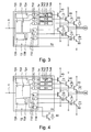
- FIG. 3 shows a circuit arrangement according to the invention for driving power semiconductor switches for a three-phase bridge circuit of the circuit breaker.
- the three-phase bridge circuit is constructed of three half-bridge circuits identical to those in FIG.
- the three-phase bridge circuit has three TOP and three BOT switches, which are also designed as IGBTs of the 1200V voltage class.
- the load (60) can be configured, for example, as a three-phase electric motor.
- the control signals (5) of the higher-level control are processed according to the invention by a single component (70) and supplied to the gates of the respective power switches (40, 50) of the three-phase bridge circuit.
- the module (70) in turn consists of four drive chips (72, 74), which are arranged isolated from each other in a common housing (70).
- the first drive chip (72) is shown here in a higher complexity compared with FIG. 2 and comprises the functional groups voltage regulator (724) input interface (720), processing logic (722), fault management (726) and protection circuit (728) as well as three drivers (732 ) for the BOT switches (50) and three level shifters (730) for the TOP switches (40) of the three-phase bridge circuit.
- the outputs of the level shifters (730) are connected to the inputs of three second drive chips (74). These each comprise a level shifter (740), a signal reconstruction (742), a processing logic and a protection circuit (744) and the driver (746) of the respective TOP switch (40).
- the signal between the processing logic (722) and the driver (746) of the TOP switch (40) is in turn by means of second level shifter (730, 740) to the necessary Potential raised.
- the first level shifter (730) is an integral part of the first drive chip (72) and the second level shifter (740) an integral part of the respective second drive chip (74), wherein the output potential of the respective second drive chips (74) in operation at different potential between 600V and 1200V and this potential fluctuates during operation.
- FIG. 4 shows a circuit arrangement according to the invention for driving power semiconductor switches for a three-phase bridge circuit with a brake chopper.
- a seventh power switch (80) is arranged in addition to the three TOP and the three BOT switches (50).
- This seventh switch (80) is used in operation as a control for a so-called. Bremschopper, which serves the removal of excess electrical energy in a circuit example of the return of the electric motor (60).
- the first drive chip has an additional driver (734) compared to that shown in FIG. 3, which is at the same potential as the drivers (732) of the BOT switches (50).
Landscapes
- Electronic Switches (AREA)
- Semiconductor Integrated Circuits (AREA)
- Metal-Oxide And Bipolar Metal-Oxide Semiconductor Integrated Circuits (AREA)
- Power Conversion In General (AREA)
Applications Claiming Priority (1)
| Application Number | Priority Date | Filing Date | Title |
|---|---|---|---|
| DE102004049817A DE102004049817A1 (de) | 2004-10-13 | 2004-10-13 | Integrierte Schaltungsanordnung zur Ansteuerung von Leistungshalbleiterschaltern |
Publications (1)
| Publication Number | Publication Date |
|---|---|
| EP1648086A1 true EP1648086A1 (fr) | 2006-04-19 |
Family
ID=35539339
Family Applications (1)
| Application Number | Title | Priority Date | Filing Date |
|---|---|---|---|
| EP05017562A Withdrawn EP1648086A1 (fr) | 2004-10-13 | 2005-08-12 | Circuit intégré pour la commande de commutateurs de puissance semi-conducteurs |
Country Status (6)
| Country | Link |
|---|---|
| US (1) | US20060087260A1 (fr) |
| EP (1) | EP1648086A1 (fr) |
| JP (1) | JP2006115472A (fr) |
| KR (1) | KR100723373B1 (fr) |
| CN (1) | CN1855679A (fr) |
| DE (1) | DE102004049817A1 (fr) |
Cited By (1)
| Publication number | Priority date | Publication date | Assignee | Title |
|---|---|---|---|---|
| US20240333267A1 (en) * | 2023-03-28 | 2024-10-03 | Epirus, Inc. | Systems and methods for high-voltage power integrated circuits |
Families Citing this family (5)
| Publication number | Priority date | Publication date | Assignee | Title |
|---|---|---|---|---|
| DE102005023652B3 (de) * | 2005-05-23 | 2006-08-03 | Semikron Elektronik Gmbh & Co. Kg | Schaltungsanordnung mit Fehlererkennung zur Ansteuerung von Leistungshalbleiterschaltern und zugehöriges Verfahren |
| DE102006050913B4 (de) * | 2006-10-28 | 2012-08-23 | Semikron Elektronik Gmbh & Co. Kg | Ansteuerschaltung mit BOT-Levelshifter zur Übertragung eines Eingangssignals und zugeordnetes Verfahren |
| DE102007006319B4 (de) * | 2007-02-08 | 2012-12-13 | Semikron Elektronik Gmbh & Co. Kg | Ansteuerschaltung mit TOP-Levelshifter zur Übertragung eines Eingangssignals und zugeordnetes Verfahren |
| US7977887B2 (en) * | 2008-09-09 | 2011-07-12 | Delphi Technologies, Inc. | Low leakage current LED drive apparatus with fault protection and diagnostics |
| US9678524B2 (en) * | 2015-09-25 | 2017-06-13 | Micron Technology, Inc. | Apparatuses and methods for power regulation based on input power |
Citations (4)
| Publication number | Priority date | Publication date | Assignee | Title |
|---|---|---|---|---|
| DE19611401A1 (de) * | 1996-03-22 | 1997-09-25 | Danfoss As | Frequenzumrichter für einen Elektromotor |
| US6114883A (en) * | 1997-07-15 | 2000-09-05 | Dialog Semiconductor Gmbh | Circuit for driving semiconductor switches |
| US6680630B1 (en) * | 2002-08-08 | 2004-01-20 | Mitsubishi Denki Kabushiki Kaisha | Driver circuit for power device |
| US6781423B1 (en) * | 2003-07-04 | 2004-08-24 | Dialog Semiconductor Gmbh | High-voltage interface and driver control circuit |
Family Cites Families (6)
| Publication number | Priority date | Publication date | Assignee | Title |
|---|---|---|---|---|
| JP2763237B2 (ja) * | 1992-11-02 | 1998-06-11 | 株式会社日立製作所 | レベルシフト回路及びこれを用いたインバータ装置 |
| JP3493313B2 (ja) * | 1998-12-07 | 2004-02-03 | シャープ株式会社 | 負電圧レベルシフタ回路および不揮発性半導体記憶装置 |
| US6507226B2 (en) * | 2000-07-31 | 2003-01-14 | Intersil Americas Inc. | Power device driving circuit and associated methods |
| JP4462776B2 (ja) * | 2001-03-13 | 2010-05-12 | 三菱電機株式会社 | 電力変換装置および信号レベル変換装置 |
| JP3806644B2 (ja) * | 2001-12-13 | 2006-08-09 | 三菱電機株式会社 | 電力用半導体装置 |
| US6531895B1 (en) * | 2002-02-08 | 2003-03-11 | Delphi Technologies, Inc. | Isolated gate drive circuit having a switched input capacitor |
-
2004
- 2004-10-13 DE DE102004049817A patent/DE102004049817A1/de not_active Ceased
-
2005
- 2005-08-12 EP EP05017562A patent/EP1648086A1/fr not_active Withdrawn
- 2005-08-15 JP JP2005235322A patent/JP2006115472A/ja active Pending
- 2005-10-05 KR KR1020050093532A patent/KR100723373B1/ko not_active Expired - Fee Related
- 2005-10-11 US US11/247,319 patent/US20060087260A1/en not_active Abandoned
- 2005-10-12 CN CNA2005101067739A patent/CN1855679A/zh active Pending
Patent Citations (4)
| Publication number | Priority date | Publication date | Assignee | Title |
|---|---|---|---|---|
| DE19611401A1 (de) * | 1996-03-22 | 1997-09-25 | Danfoss As | Frequenzumrichter für einen Elektromotor |
| US6114883A (en) * | 1997-07-15 | 2000-09-05 | Dialog Semiconductor Gmbh | Circuit for driving semiconductor switches |
| US6680630B1 (en) * | 2002-08-08 | 2004-01-20 | Mitsubishi Denki Kabushiki Kaisha | Driver circuit for power device |
| US6781423B1 (en) * | 2003-07-04 | 2004-08-24 | Dialog Semiconductor Gmbh | High-voltage interface and driver control circuit |
Non-Patent Citations (1)
| Title |
|---|
| LIN R L ET AL: "Single-power-supply-based transformerless IGBT/MOSFET gate driver with 100% high-side turn-on duty cycle operation performance using auxiliary bootstrapped charge pumper", POWER ELECTRONICS SPECIALISTS CONFERENCE, 1997. PESC '97 RECORD., 28TH ANNUAL IEEE ST. LOUIS, MO, USA 22-27 JUNE 1997, NEW YORK, NY, USA,IEEE, US, vol. 2, 22 June 1997 (1997-06-22), pages 1205 - 1209, XP010241701, ISBN: 0-7803-3840-5 * |
Cited By (1)
| Publication number | Priority date | Publication date | Assignee | Title |
|---|---|---|---|---|
| US20240333267A1 (en) * | 2023-03-28 | 2024-10-03 | Epirus, Inc. | Systems and methods for high-voltage power integrated circuits |
Also Published As
| Publication number | Publication date |
|---|---|
| CN1855679A (zh) | 2006-11-01 |
| KR20060052050A (ko) | 2006-05-19 |
| KR100723373B1 (ko) | 2007-05-30 |
| JP2006115472A (ja) | 2006-04-27 |
| US20060087260A1 (en) | 2006-04-27 |
| DE102004049817A1 (de) | 2006-04-27 |
Similar Documents
| Publication | Publication Date | Title |
|---|---|---|
| EP1920526B1 (fr) | Montage convertisseur a accumulateurs d'energie repartis | |
| EP1887698B1 (fr) | Modificateur de niveau pour un commutateur de commande pour composants semi-conducteurs de puissance | |
| DE112014003605B4 (de) | Antriebssteuerungsvorrichtung für einen elektrischen Motor | |
| DE102010018997B4 (de) | Ansteuerschaltung mit Übertragungsschaltung zur kapazitiven Übertragung eines Signals und zugeordnetes Verfahren | |
| DE102007006319A1 (de) | Ansteuerschaltung mit TOP-Levelshifter zur Übertragung eines Eingangssignals und zugeordnetes Verfahren | |
| DE102013224022A1 (de) | Wechselrichter mit SiC-JFETs | |
| DE102011055626A1 (de) | Phasentrennung bei eps-systemen | |
| EP2705589A2 (fr) | Batterie comprenant au moins une suite de modules | |
| EP2871766B1 (fr) | Commutateur de commande pour onduleur à trois niveaux | |
| DE102004059313B3 (de) | Leistungshalbleitermodul mit verringerten parasitären Induktivitäten | |
| WO2015117691A1 (fr) | Circuit redresseur à transistor autobloquant | |
| EP2871763B1 (fr) | Système de commande de circuits en pont doté de circuit intermédiaire mis à la terre symétriquement | |
| EP2705598A2 (fr) | Unité d'entraînement pour moteur électrique | |
| DE10221081A1 (de) | Wechselrichter für eine elektrische Maschine | |
| DE112018006066T5 (de) | Steuerschaltung für einen Mehrphasenmotor | |
| EP2824837B1 (fr) | Commutateur semi-conducteur de puissance | |
| EP1648086A1 (fr) | Circuit intégré pour la commande de commutateurs de puissance semi-conducteurs | |
| EP1739835B1 (fr) | Circuit pour la commande de commutateurs semi-conducteurs de puissance avec détection d'erreur | |
| DE102017203233A1 (de) | Modularer Wechselrichter | |
| DE102016207254A1 (de) | Wechselrichter, elektrische Antriebsanordnung mit einem Wechselrichter | |
| WO2022263233A1 (fr) | Système de barres conductrices à basse impédance entre un module de demi-pont et un circuit intermédiaire | |
| DE102020007476A1 (de) | Wechselrichter zur Ansteuerung eines Elektromotors eines elektrisch antreibbaren Fahrzeugs | |
| EP2590314A1 (fr) | Onduleur et système électronique de puissance doté de tels systèmes onduleurs | |
| EP0366892A2 (fr) | Circuit de commande pour un moteur à courant continu sans balais | |
| EP3462615A1 (fr) | Structures en cascode optimisées |
Legal Events
| Date | Code | Title | Description |
|---|---|---|---|
| PUAI | Public reference made under article 153(3) epc to a published international application that has entered the european phase |
Free format text: ORIGINAL CODE: 0009012 |
|
| AK | Designated contracting states |
Kind code of ref document: A1 Designated state(s): AT BE BG CH CY CZ DE DK EE ES FI FR GB GR HU IE IS IT LI LT LU LV MC NL PL PT RO SE SI SK TR |
|
| AX | Request for extension of the european patent |
Extension state: AL BA HR MK YU |
|
| AKX | Designation fees paid |
Designated state(s): AT BE BG CH CY CZ DE DK EE ES FI FR GB GR HU IE IS IT LI LT LU LV MC NL PL PT RO SE SI SK TR |
|
| STAA | Information on the status of an ep patent application or granted ep patent |
Free format text: STATUS: THE APPLICATION IS DEEMED TO BE WITHDRAWN |
|
| 18D | Application deemed to be withdrawn |
Effective date: 20061020 |