EP1648101B1 - Circuit de réception pour un dispositif de réception optique - Google Patents
Circuit de réception pour un dispositif de réception optique Download PDFInfo
- Publication number
- EP1648101B1 EP1648101B1 EP20040024681 EP04024681A EP1648101B1 EP 1648101 B1 EP1648101 B1 EP 1648101B1 EP 20040024681 EP20040024681 EP 20040024681 EP 04024681 A EP04024681 A EP 04024681A EP 1648101 B1 EP1648101 B1 EP 1648101B1
- Authority
- EP
- European Patent Office
- Prior art keywords
- receiver
- electrical
- circuit according
- optical
- photodiode
- Prior art date
- Legal status (The legal status is an assumption and is not a legal conclusion. Google has not performed a legal analysis and makes no representation as to the accuracy of the status listed.)
- Expired - Lifetime
Links
- 230000003287 optical effect Effects 0.000 title claims description 38
- 238000011156 evaluation Methods 0.000 claims description 23
- 230000006399 behavior Effects 0.000 claims description 8
- 238000012544 monitoring process Methods 0.000 claims description 4
- 238000005286 illumination Methods 0.000 claims description 3
- 230000002452 interceptive effect Effects 0.000 claims description 2
- 238000000034 method Methods 0.000 claims 1
- 238000012806 monitoring device Methods 0.000 claims 1
- 102100039435 C-X-C motif chemokine 17 Human genes 0.000 description 3
- 101000889048 Homo sapiens C-X-C motif chemokine 17 Proteins 0.000 description 3
- 239000003990 capacitor Substances 0.000 description 3
- 238000001514 detection method Methods 0.000 description 2
- 238000012545 processing Methods 0.000 description 2
- 230000004044 response Effects 0.000 description 2
- 230000001629 suppression Effects 0.000 description 2
- 230000006978 adaptation Effects 0.000 description 1
- 230000005540 biological transmission Effects 0.000 description 1
- 238000012937 correction Methods 0.000 description 1
- 230000008878 coupling Effects 0.000 description 1
- 238000010168 coupling process Methods 0.000 description 1
- 238000005859 coupling reaction Methods 0.000 description 1
- 230000007423 decrease Effects 0.000 description 1
- 238000013461 design Methods 0.000 description 1
- 230000000694 effects Effects 0.000 description 1
- 239000000835 fiber Substances 0.000 description 1
- 230000010354 integration Effects 0.000 description 1
- 238000002360 preparation method Methods 0.000 description 1
- 238000005070 sampling Methods 0.000 description 1
- 239000004065 semiconductor Substances 0.000 description 1
Images


Classifications
-
- H—ELECTRICITY
- H04—ELECTRIC COMMUNICATION TECHNIQUE
- H04B—TRANSMISSION
- H04B10/00—Transmission systems employing electromagnetic waves other than radio-waves, e.g. infrared, visible or ultraviolet light, or employing corpuscular radiation, e.g. quantum communication
- H04B10/60—Receivers
- H04B10/66—Non-coherent receivers, e.g. using direct detection
Definitions
- the invention relates to a receiving circuit for an optical receiving device according to the preamble of claim 1.
- photodiodes larger diameter of, for example, 1 mm and higher temperatures of, for example, greater than 100 ° C, as used in particular in plastic fiber systems in the automotive sector, occurring dark currents can increase significantly and make an evaluation of the photodiode current impossible because of the required accuracy .
- An evaluation of the photodiode current takes place, for example, for the purpose of monitoring the optical power or for a sleep mode control.
- FIG. 3 shows by means of some examples, the dark currents of known photodiodes of larger diameter as a function of the temperature.
- the dark currents increase exponentially towards higher temperatures and at high temperatures may be well above the currents of the minimum regular input powers of the signal to be detected.
- the problem of dark currents occurring can be reduced with regard to the evaluation of the data contained in a modulated optical signal, for example by offset correction circuits.
- the noise influence of the dark current is negligible in terms of data transmission.
- the solution according to the invention is characterized by the idea of providing an optical receiving device and, in addition, an electrical element reproducing the receiving device in the absence of illumination, to average the signals provided by the optical receiving device and to evaluate the difference between the two electrical signals.
- the difference between the time-averaged electrical signal of the optical receiving device and the electrical signal of the electrical element is detected.
- the electrical element in particular detects dark currents and other interference signals which are superimposed on the useful signal to be detected by the optical receiving device.
- the electrical element simulates the electrical behavior of the first receiving device in the absence of illumination, the dark currents of the two components are substantially identical and can be subtracted, ie the difference between the average values of the two output signals from the optical receiving device and the electrical element can be evaluated or detected very exactly the input power at the optical receiving device.
- a “lighting-free case” is understood to mean that the electrical element behaves electrically as much as the receiving device when no light to be detected impinges on the receiving device.
- the means for detecting the difference between the two time-averaged signals have current mirrors which subtract a noise component of the electrical signal of the optical receiving device from the electrical signal of the optical receiving device.
- the electrical signal of the electrical element is averaged and detects the difference between the two time-averaged electrical signals.
- This symmetrical structure of the receiving circuit has the advantage that the side of the supply voltage, the interference suppression is improved.
- the electrical element simulating the electrical behavior of the receiving device in the lighting-free case can be, for example, a receiving device ("dummy receiving device") identical to the receiving device ("payload receiving device") of the receiver circuit, which is darkened in such a way that no light is emitted can fall on it.
- the "utility" receiving device and the "dummy” receiving device are preferably jointly monolithically integrated on a semiconductor chip in order to ensure that both receiving devices have an approximately equal electrical behavior.
- the electrical behavior of the user-receiving device in the lighting-free case reproducing electrical element may also be formed by a capacitance, which simulates the capacitive behavior of the Nutz-receiving device.
- the optical receiving device is preferably a photodiode, in particular a larger diameter photodiode of, for example, 1 mm, which is used at higher temperatures.
- the electrical element is preferably also a photodiode, which is designed to be similar to the first photodiode.
- the two photodiodes are monolithically integrated on a chip. Due to the similarity of the two photodiodes and the monolithic integration, it is possible to assume that the dark currents that are largely the same are eliminated by the subtraction. The error in the differential evaluation is about 1 to 5% of the absolute dark current.
- a preferred application of the present invention is the evaluation of the input power to the first photodiode, for example, for monitoring the optical power or for a sleep mode control. Due to the inventive detection of the difference of the two time-averaged signals, a reliable evaluation of the input power can be made even with photodiodes of large diameter and at high temperatures, which are characterized by high dark currents.
- an evaluation circuit is provided which the recorded electrical signal of the optical receiving device and the electrical signal of the electrical element and processed for further evaluation.
- the means for detecting the difference of the two time-averaged signals additionally comprise a differential amplifier.
- the processed by the evaluation electrical signals of the optical receiving device and the electrical element are supplied to the two inputs of the differential amplifier.
- the at least one evaluation circuit preferably has resistors at each of which a voltage is tapped off and supplied to the two inputs of the differential amplifier.
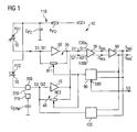
- FIG. 1 If one recognizes a photodiode 10 as a receiving device ("Nutz" -Empfangsbeaten), which is connected via a transimpedance amplifier 20 to a terminal E30a of a differential amplifier 30.
- the other input E30b of the differential amplifier 30 is connected via a further designed as a transimpedance amplifier preamplifier 40 with a "dummy" photodiode 50 as a “dummy” -connected, which electrically simulates the electrical behavior of the receiving device 10 in the lighting-free case.
- the transimpedance amplifier 20 is formed by a voltage amplifier 60, for example an operational amplifier, which is connected to a feedback resistor RF1.
- the differential amplifier 30 has its output connected to a second differential amplifier 80, which further amplifies the output signal of the first differential amplifier 30 and generates at its output an optical signal of the photodiode 10 corresponding output signal S res 'or the inverted signal -S res '.
- the differential amplifier 80 is connected to an AGC (Amplitude Gain Control) control circuit 90, whose output side is connected to the two feedback resistors RF1 and RF2.
- the control circuit 90 sets the resistance value RF1 and RF2 in response to a control signal S3 applied to a control input S90 of the control circuit 90.
- control circuit 90 may also include additional capacitances (or inductors) in parallel or in series with the two feedback resistors RF1 and RF2 switch to modify the feedback behavior and, for example, to avoid the occurrence of electrical vibrations.
- control circuit 90 is supplied with the output signals Sres 'and -Sres' of the second amplifier 80, so that the control circuit can prevent, for example, overdriving the amplifier.
- the optical receiver circuit is equipped with a DCC (Duty Cycle Control) circuit 100 which effects control of the optical receiver circuit.
- the DCC circuit 100 or the duty cycle control formed by it (offset control) regulates the sampling threshold for the following differential amplifiers, so that the signal is sampled at the 50% value of the amplitude and thus no signal pulse distortions (duty cycle ). This can be done by feeding a current in each one of the preamplifier (transimpedance amplifier) or by feeding a voltage to the inputs of the differential amplifier directly.
- the two photodiodes 10 and 50 are both connected to a supply voltage VCC1, which is connected to a low-pass filter 110 consisting of a capacitor C PD and a resistor R PD .
- the optical receiver circuit is operated as follows:
- an electrical signal S1 is fed into the transimpedance amplifier 20 and amplified by this.
- the amplified signal S1 ' is thus formed, which arrives at the input E30a of the differential amplifier 30.
- Noise signals St1 which are coupled or fed into the photodiode 10 or into the supply lines of the photodiode 10 are also amplified by the transimpedance amplifier 20 and transmitted as amplified interference signals St1 'to the differential amplifier 30.
- the dummy photodiode 50 is - as the vertical bar in the FIG. 1 indicated - darkened so that no light can fall on the dummy photodiode 50.
- the photodiode 50 is thus optically inactive and has only the function of a "dummy".
- interference signals ST2 can be coupled into the "dummy" photodiode, for example via the supply lines of the photodiode 50.
- These interference signals ST2 are amplified by the further transimpedance amplifier 40 and pass as amplified interference signals ST2 'to the further input E30b of the differential amplifier 30.
- the low-pass filter 110 at the power supply voltage VCC1 serves, moreover, to filter out high-frequency interference of the power supply VCC1, so that higher-frequency interference is additionally suppressed, since usually the common mode interference suppression decreases at high frequencies.
- connection pads 200 and 210 can be seen, which can be connected to one another by means of a bonding wire 220.
- the capacitance C SYM can be connected to the further transimpedance amplifier 40.
- the capacitance C SYM can replace the "dummy" photodiode 50, if such a photodiode 50 is not available.
- the capacitance C SYM is then preferably dimensioned such that it substantially corresponds to the capacitance of the "missing" dummy photodiode 50 or the capacitance of the useful diode 10.
- optical receiving circuit relates to the preparation of a received signal with respect to the data contained in the signal, which evaluates in the FIG. 2 illustrated arrangement of the output from the two photodiodes 10, 50 signal with respect to the input power.
- the anode terminals of the two photodiodes 10, 50 corresponding to those in the FIG. 1 shown receiving circuit respectively connected to a transimpedance amplifier 60, 70, wherein the output of a transimpedance amplifier 60, the actual useful signal and the output of the other transimpedance amplifier 70 provides a reference signal.
- This circuit part not shown in further detail, for example, according to the FIG. 1 be designed. However, other receiving circuits may also be connected. It is also conceivable in principle not to evaluate the signal applied to the anode terminals of the photodiodes 10, 50 at all.
- the two photodiodes 10 are integrated on a common chip 400.
- the cathode terminals of the photodiodes 10, 20 are each connected to the one terminal of a capacitor C PD1 , C PD2 , whose other terminal is connected to a reference potential such as ground.
- the cathode connections are furthermore connected via evaluation circuits 310, 320 to the two inputs E330a, E330b of a differential amplifier 330.
- the output of the differential amplifier 330 is connected to evaluation units 340, 350, which are shown schematically, and which are, for example, an optical power monotoring unit 340 and / or a sleep mode controller 350.
- the latter comprises a device 351 which outputs a "sleep state” or a “wake state” in response to the presence of an input signal, and a power supply 352 which provides the power supply according to the output state of the device 351 according to a normal mode or a sleep mode , Upon detection of an optical signal by the photodiode 10, the "sleep state" is terminated.
- the operation of the circuit is as follows.
- the output of the uncovered photodiode 10 is from the capacitance C PD1 , which acts as an integrator, averaged.
- the capacitance C PD1 is thereby charged and discharged by the fluctuating in intensity photocurrent signals of the photodiode 10 and adjusts itself to an average value by which it varies at most slightly.
- the evaluation circuit 310 prepares the averaged photocurrent signal with a corresponding dynamic so that it is supplied to the non-inverting input E330b of the differential amplifier 230.
- the output signal of the covered, non-illuminated photodiode 50 which is similar to the photodiode 10, is averaged (if it is not constant anyway) by means of the capacitance C PD2 and fed to the second evaluation circuit 320. This prepares this signal with the appropriate dynamics, so that it can be fed to the inverting input E330a of the differential amplifier.
- the differential amplifier 330 subtracts the dark current of the covered photodiode 50 from the signal of the active photodiode 10. In this way, the dark currents can be eliminated. These can be at values of up to 1 ⁇ A at high temperatures and large photodiode areas, while the currents to be evaluated are only 0.1 pA.
- FIG. 2 described circuit with the evaluation circuits 310, 320 and the differential amplifier 330 in principle also at the anode terminals of the photodiodes 10, 50 can be realized. Likewise, the arrangement of the FIG. 1 also take place at the cathode terminals of the photodiodes 10, 50. Associated minor adaptations of the circuits are familiar to the expert.
- FIGS. 4 and 5 show exemplary embodiments of the design of the evaluation circuits 310, 320.
- the evaluation circuits 310, 320 can be realized in particular with current mirrors or by means of resistors, at which a voltage is tapped.
- FIG. 4 are the two circuits 310, 320 of the FIG. 2 integrated into a common circuit 300, which has two resistors R1, R2, at each of which a voltage is tapped.
- the tapped voltage is supplied to a known subtraction circuit with resistors R3, R4, R5, R6 and a differential amplifier 330. Only the difference of the input voltages at the inverting input E330a and at the non-inverting input E330b is amplified.
- FIG. 5 there is a subtraction of the averaged photodiode currents of the photodiodes 10, 50 by means of a current mirror circuit, without a differential amplifier is required. This is achieved by a chain of several current mirrors.
- a first current mirror is provided by p-channel transistors T1, T2, a second current mirror by P-channel transistors T3, T4 and a third current mirror by n-channel transistors T5, T6.
- the gate terminal and the drain terminal of the transistor T1 are connected to the cathode terminal of the illuminated photodiode 10 (the integrating capacitor is in the FIGS. 4 and 5 for better clarity, not shown separately).
- the source terminal of the transistor T1 is - optionally via a resistor - connected to a supply voltage.
- the gate terminals of the transistors T1 and T2 are connected together.
- the source terminal of the transistor T2 is - optionally also via a resistor - also connected to the supply voltage.
- the operation of the current mirror is as follows.
- the current I PD1 generated by the photodiode 10 represents a reference current of the current mirror flowing through the transistor T1.
- This reference current I PD1 consists of two components I PD and I D1 , namely the actual photodiode current I PD to be detected and the dark current I D1 applied to the photodiode 10.
- the current mirror now generates a control current which is in a specific relationship to the reference current and which flows through the transistor T2.
- the setting is such that the reference current is mirrored identically to the transistor T2 through the photodiode 10, flows through it and is output at the drain terminal.
- the photodiode current I PD2 of the covered photodiode 50 which consists solely of the dark current I D2 of this photodiode, is mirrored via the mirror circuit T4, T3 constructed in the same way to the drain terminal of the transistor T3.
- the current flowing through the transistor T3 current ID2 is now again the reference current of the further current mirror consisting of the transistors T6, T5 and is mirrored accordingly to the current through the transistor T5.
- the capacitances C PD1 and C PD2 in the embodiment of the FIG. 4 parallel to the resistors R5 and R6 be formed.
- Another alternative is to have a capacity at node A of FIG. 5 train.
Landscapes
- Physics & Mathematics (AREA)
- Electromagnetism (AREA)
- Engineering & Computer Science (AREA)
- Computer Networks & Wireless Communication (AREA)
- Signal Processing (AREA)
- Amplifiers (AREA)
Claims (13)
- Circuit de réception pour un dispositif de réception (95) optique avec- un dispositif (10) de réception optique, qui transforme un signal optique en un signal électrique,- un élément (50) électrique imitant le comportement électrique d'un dispositif (10) de réception dans un cas sans éclairage,caractérisé par- un premier système (CPD1) à circuit, qui fournit le signal électrique au dispositif (10) de réception optique, et- des moyens (330 ; T1 à T6) pour détecter la différence entre le signal électrique fourni dans le temps et le signal électrique de l'élément (50) électrique,- ces moyens (330, T1à T6) présentant des miroirs (T1, T2, T3, T4, T5, T6) de courant, qui soustraient une composante perturbatrice du signal électrique du dispositif de réception optique (10) à partir du signal électrique du dispositif de réception optique (10).
- Circuit de réception selon la revendication 1, caractérisé en ce que l'élément (50) électrique est formé par un autre dispositif de réception foncé.
- Circuit de réception selon la revendication 2, caractérisé en ce que le dispositif (10) de réception et l'autre dispositif (50) de réception sont intégrés de manière monolithique sur une puce.
- Circuit de réception selon la revendication 2 ou 3, caractérisé en ce que les deux dispositifs (10, 50) sont des photodiodes.
- Circuit de réception selon l'une quelconque des revendications précédentes, caractérisé par au moins un circuit (300, 310, 320) d'interprétation, qui détecte le signal électrique du dispositif (10) de réception et le signal électrique de l'élément (50) électrique et traite une autre interprétation.
- Circuit de réception selon l'une quelconque des revendications précédentes, caractérisé en ce que les moyens de détection de la différence des deux signaux électriques comprennent en plus un amplificateur (330) différentiel.
- Circuit de réception selon les revendications 5 et 6, caractérisé en ce que les signaux électriques traités du dispositif (10) de réception optique et de l'élément (50) électrique sont acheminés dans les deux entrées (E330a, E330b) de l'amplificateur (330) différentiel.
- Circuit de réception selon la revendication 7, caractérisé en ce qu'au moins le parmi un circuit (300) d'interprétation présente des résistances (R1, R2), au niveau de chacune desquelles est prélevée une tension qui est amenée aux deux entrées (E330a, E330b) de l'amplificateur (330) différentiel.
- Circuit de réception selon l'une quelconque des revendications précédentes, caractérisé en ce que les moyens (330, T1 à T6) de détection de la différence des deux signaux électriques sont reliés à une commande (350) de mode veille.
- Circuit de réception selon l'une quelconque des revendications précédentes, caractérisé en ce que les moyens (330, T1 à T6) de détection de la différence des deux signaux électriques sont reliés à un dispositif (340) de contrôle afin de contrôler la puissance optique reçue par le dispositif (10) de réception.
- Circuit de réception selon l'une quelconque des revendications précédentes, caractérisé en ce qu'un second système (CPD2) à circuit fournit le signal électrique de l'élément (50) électrique, les moyens (330, T1 à T6) de détection de différence détectant la différence des deux signaux électriques fournis dans le temps.
- Circuit de réception selon l'une des revendications précédentes, caractérisé en ce que le premier système (CPD1) à circuit est formé par une capacitance.
- Circuit de réception selon l'une des revendications précédentes, caractérisé en ce que le second système (CPD2) à circuit est formé par une capacitance.
Priority Applications (2)
| Application Number | Priority Date | Filing Date | Title |
|---|---|---|---|
| EP20040024681 EP1648101B1 (fr) | 2004-10-15 | 2004-10-15 | Circuit de réception pour un dispositif de réception optique |
| DE200450007397 DE502004007397D1 (de) | 2004-10-15 | 2004-10-15 | Empfangsschaltung für eine optische Empfangseinrichtung |
Applications Claiming Priority (1)
| Application Number | Priority Date | Filing Date | Title |
|---|---|---|---|
| EP20040024681 EP1648101B1 (fr) | 2004-10-15 | 2004-10-15 | Circuit de réception pour un dispositif de réception optique |
Publications (2)
| Publication Number | Publication Date |
|---|---|
| EP1648101A1 EP1648101A1 (fr) | 2006-04-19 |
| EP1648101B1 true EP1648101B1 (fr) | 2008-06-18 |
Family
ID=34927007
Family Applications (1)
| Application Number | Title | Priority Date | Filing Date |
|---|---|---|---|
| EP20040024681 Expired - Lifetime EP1648101B1 (fr) | 2004-10-15 | 2004-10-15 | Circuit de réception pour un dispositif de réception optique |
Country Status (2)
| Country | Link |
|---|---|
| EP (1) | EP1648101B1 (fr) |
| DE (1) | DE502004007397D1 (fr) |
Families Citing this family (2)
| Publication number | Priority date | Publication date | Assignee | Title |
|---|---|---|---|---|
| CN106781424B (zh) * | 2017-01-09 | 2024-06-21 | 上海胤祺集成电路有限公司 | 红外接收电路 |
| CN116961773A (zh) * | 2022-04-15 | 2023-10-27 | 华为技术有限公司 | 一种光接收机 |
Family Cites Families (4)
| Publication number | Priority date | Publication date | Assignee | Title |
|---|---|---|---|---|
| JP3207240B2 (ja) * | 1992-04-10 | 2001-09-10 | キヤノン株式会社 | フォトダイオードのバイアス回路 |
| US5410145A (en) * | 1994-02-25 | 1995-04-25 | Coroy; Trenton G. | Light detector using reverse biased photodiodes with dark current compensation |
| DE19821865A1 (de) * | 1998-05-15 | 1999-11-18 | Siemens Ag | Empfängerschaltung für ein optisches Signal sowie Einrichtung zur Datenübertragung mit einer derartigen Empfängerschaltung |
| JP3775574B2 (ja) * | 2001-05-22 | 2006-05-17 | シャープ株式会社 | 光結合装置 |
-
2004
- 2004-10-15 DE DE200450007397 patent/DE502004007397D1/de not_active Expired - Fee Related
- 2004-10-15 EP EP20040024681 patent/EP1648101B1/fr not_active Expired - Lifetime
Also Published As
| Publication number | Publication date |
|---|---|
| DE502004007397D1 (de) | 2008-07-31 |
| EP1648101A1 (fr) | 2006-04-19 |
Similar Documents
| Publication | Publication Date | Title |
|---|---|---|
| EP1511198B1 (fr) | Circuit récepteur optique | |
| DE19753472B4 (de) | Photoelektrische Zelle mit stabilisierter Verstärkung | |
| EP1545029B1 (fr) | Dispositif de réception optique | |
| DE2429953A1 (de) | Schaltungsanordnung zur verarbeitung physiologischer messignale | |
| DE10232346B4 (de) | Schaltungsanordnung und Verfahren zur Datensignalreproduktion | |
| EP3339820A1 (fr) | Récepteur de lumière et procédé de lecture de photodiodes à avalanche | |
| DE3620931A1 (de) | Empfaenger fuer optische digitalsignale | |
| DE69018516T2 (de) | Optische Empfänger. | |
| EP1545028B1 (fr) | Récepteur optique avec dispositif de commande avec un largeur de bande variable | |
| DE102010013318B4 (de) | Verstärkerschaltung, Detektoranordnung und Verfahren zum Betreiben eines Verstärkers | |
| WO1995021371A1 (fr) | Circuit pour la reception de signaux lumineux | |
| DE102017127963A1 (de) | Schaltungsanordnung zum Erfassen von Licht | |
| EP3631978B1 (fr) | Circuit à amplificateur à transimpédance | |
| EP1648101B1 (fr) | Circuit de réception pour un dispositif de réception optique | |
| EP1319965A2 (fr) | Circuit d'évaluation et méthode de traitement de signal | |
| DE69129780T2 (de) | Infrarotstrahlungsempfangsschaltung | |
| EP0643496A1 (fr) | Récepteur optique avec amplificateur adaptation d'impédance à gamme dynamique étendue | |
| DE102005013494B4 (de) | Optischer Empfänger | |
| DE4212934A1 (de) | Schaltungsanordnung für einen optischen Empfänger | |
| DE2720614C3 (de) | Breitbandverstärker für Fotodioden | |
| DE10029609A1 (de) | Hochgeschwindigkeits-Optokoppler-Detektor | |
| EP4495483B1 (fr) | Dispositif de détection de flamme et procédé de fonctionnement d'un dispositif de détection de flamme | |
| DE69222618T2 (de) | Vorverstärker für einen optischen Empfänger | |
| DE69225833T2 (de) | Optischer Sender | |
| EP3036561B1 (fr) | Dispositif à compensation d'effets parasites pour mesurer un trajet de transmission optique |
Legal Events
| Date | Code | Title | Description |
|---|---|---|---|
| PUAI | Public reference made under article 153(3) epc to a published international application that has entered the european phase |
Free format text: ORIGINAL CODE: 0009012 |
|
| 17P | Request for examination filed |
Effective date: 20051206 |
|
| AK | Designated contracting states |
Kind code of ref document: A1 Designated state(s): AT BE BG CH CY CZ DE DK EE ES FI FR GB GR HU IE IT LI LU MC NL PL PT RO SE SI SK TR |
|
| AX | Request for extension of the european patent |
Extension state: AL HR LT LV MK |
|
| RAP1 | Party data changed (applicant data changed or rights of an application transferred) |
Owner name: INFINEON TECHNOLOGIES AG |
|
| AKX | Designation fees paid |
Designated state(s): DE FR GB |
|
| GRAP | Despatch of communication of intention to grant a patent |
Free format text: ORIGINAL CODE: EPIDOSNIGR1 |
|
| RAP1 | Party data changed (applicant data changed or rights of an application transferred) |
Owner name: AVAGO TECHNOLOGIES FIBER IP (SINGAPORE) PTE. LTD. |
|
| GRAS | Grant fee paid |
Free format text: ORIGINAL CODE: EPIDOSNIGR3 |
|
| GRAA | (expected) grant |
Free format text: ORIGINAL CODE: 0009210 |
|
| AK | Designated contracting states |
Kind code of ref document: B1 Designated state(s): DE FR GB |
|
| REG | Reference to a national code |
Ref country code: GB Ref legal event code: FG4D Free format text: NOT ENGLISH |
|
| REF | Corresponds to: |
Ref document number: 502004007397 Country of ref document: DE Date of ref document: 20080731 Kind code of ref document: P |
|
| PLBE | No opposition filed within time limit |
Free format text: ORIGINAL CODE: 0009261 |
|
| STAA | Information on the status of an ep patent application or granted ep patent |
Free format text: STATUS: NO OPPOSITION FILED WITHIN TIME LIMIT |
|
| 26N | No opposition filed |
Effective date: 20090319 |
|
| REG | Reference to a national code |
Ref country code: FR Ref legal event code: ST Effective date: 20090630 |
|
| PG25 | Lapsed in a contracting state [announced via postgrant information from national office to epo] |
Ref country code: DE Free format text: LAPSE BECAUSE OF NON-PAYMENT OF DUE FEES Effective date: 20090501 |
|
| PG25 | Lapsed in a contracting state [announced via postgrant information from national office to epo] |
Ref country code: FR Free format text: LAPSE BECAUSE OF NON-PAYMENT OF DUE FEES Effective date: 20081031 |
|
| REG | Reference to a national code |
Ref country code: GB Ref legal event code: 732E Free format text: REGISTERED BETWEEN 20130725 AND 20130731 |
|
| PGFP | Annual fee paid to national office [announced via postgrant information from national office to epo] |
Ref country code: GB Payment date: 20150924 Year of fee payment: 12 |
|
| GBPC | Gb: european patent ceased through non-payment of renewal fee |
Effective date: 20161015 |
|
| PG25 | Lapsed in a contracting state [announced via postgrant information from national office to epo] |
Ref country code: GB Free format text: LAPSE BECAUSE OF NON-PAYMENT OF DUE FEES Effective date: 20161015 |