EP1650871A1 - Procédé et appareil pour compenser des variations du facteur de conversion charge-tension dans un détecteur - Google Patents
Procédé et appareil pour compenser des variations du facteur de conversion charge-tension dans un détecteur Download PDFInfo
- Publication number
- EP1650871A1 EP1650871A1 EP05109703A EP05109703A EP1650871A1 EP 1650871 A1 EP1650871 A1 EP 1650871A1 EP 05109703 A EP05109703 A EP 05109703A EP 05109703 A EP05109703 A EP 05109703A EP 1650871 A1 EP1650871 A1 EP 1650871A1
- Authority
- EP
- European Patent Office
- Prior art keywords
- detector
- drift
- radiation detector
- type radiation
- momentary
- Prior art date
- Legal status (The legal status is an assumption and is not a legal conclusion. Google has not performed a legal analysis and makes no representation as to the accuracy of the status listed.)
- Ceased
Links
- 238000000034 method Methods 0.000 title claims description 10
- 230000008859 change Effects 0.000 claims abstract description 30
- 230000001419 dependent effect Effects 0.000 claims abstract description 24
- 230000005855 radiation Effects 0.000 claims abstract description 21
- 230000008878 coupling Effects 0.000 claims description 12
- 238000010168 coupling process Methods 0.000 claims description 12
- 238000005859 coupling reaction Methods 0.000 claims description 12
- 230000005669 field effect Effects 0.000 claims description 8
- 238000002083 X-ray spectrum Methods 0.000 claims description 3
- 230000007274 generation of a signal involved in cell-cell signaling Effects 0.000 claims 1
- 238000005259 measurement Methods 0.000 description 9
- 239000003990 capacitor Substances 0.000 description 6
- 238000010586 diagram Methods 0.000 description 4
- XUIMIQQOPSSXEZ-UHFFFAOYSA-N Silicon Chemical compound [Si] XUIMIQQOPSSXEZ-UHFFFAOYSA-N 0.000 description 3
- 239000002800 charge carrier Substances 0.000 description 3
- 230000003247 decreasing effect Effects 0.000 description 3
- 239000004065 semiconductor Substances 0.000 description 3
- 229910052710 silicon Inorganic materials 0.000 description 3
- 239000010703 silicon Substances 0.000 description 3
- 230000003321 amplification Effects 0.000 description 2
- 230000005591 charge neutralization Effects 0.000 description 2
- 238000005516 engineering process Methods 0.000 description 2
- 230000007246 mechanism Effects 0.000 description 2
- 238000003199 nucleic acid amplification method Methods 0.000 description 2
- 238000013459 approach Methods 0.000 description 1
- 238000010276 construction Methods 0.000 description 1
- 238000012937 correction Methods 0.000 description 1
- 238000001514 detection method Methods 0.000 description 1
- 230000000694 effects Effects 0.000 description 1
- 230000005684 electric field Effects 0.000 description 1
- 230000005670 electromagnetic radiation Effects 0.000 description 1
- 239000003574 free electron Substances 0.000 description 1
- 238000005286 illumination Methods 0.000 description 1
- 238000003384 imaging method Methods 0.000 description 1
- 238000012886 linear function Methods 0.000 description 1
- 239000000463 material Substances 0.000 description 1
- 238000012544 monitoring process Methods 0.000 description 1
- 238000006386 neutralization reaction Methods 0.000 description 1
- 230000003472 neutralizing effect Effects 0.000 description 1
- 230000010355 oscillation Effects 0.000 description 1
- 230000004044 response Effects 0.000 description 1
- 102220007331 rs111033633 Human genes 0.000 description 1
- 102220067365 rs143592561 Human genes 0.000 description 1
- 238000007493 shaping process Methods 0.000 description 1
- 238000004088 simulation Methods 0.000 description 1
- 230000003595 spectral effect Effects 0.000 description 1
- 238000004611 spectroscopical analysis Methods 0.000 description 1
Images

Classifications
-
- H—ELECTRICITY
- H03—ELECTRONIC CIRCUITRY
- H03F—AMPLIFIERS
- H03F3/00—Amplifiers with only discharge tubes or only semiconductor devices as amplifying elements
- H03F3/04—Amplifiers with only discharge tubes or only semiconductor devices as amplifying elements with semiconductor devices only
- H03F3/08—Amplifiers with only discharge tubes or only semiconductor devices as amplifying elements with semiconductor devices only controlled by light
- H03F3/087—Amplifiers with only discharge tubes or only semiconductor devices as amplifying elements with semiconductor devices only controlled by light with IC amplifier blocks
-
- H—ELECTRICITY
- H03—ELECTRONIC CIRCUITRY
- H03F—AMPLIFIERS
- H03F3/00—Amplifiers with only discharge tubes or only semiconductor devices as amplifying elements
- H03F3/04—Amplifiers with only discharge tubes or only semiconductor devices as amplifying elements with semiconductor devices only
- H03F3/08—Amplifiers with only discharge tubes or only semiconductor devices as amplifying elements with semiconductor devices only controlled by light
- H03F3/082—Amplifiers with only discharge tubes or only semiconductor devices as amplifying elements with semiconductor devices only controlled by light with FET's
Definitions
- the invention concerns generally the technology of solid-state detectors for electromagnetic radiation. Especially the invention concerns a way of compensating for the shifting of peak positions as a rate of photon count rate in a drift-type detector used e.g. to detect X-rays.
- a traditional solid-state detector type to be used for X-ray detection in e.g. imaging and spectroscopy applications is the PIN detector.
- the detecting element is a reverse biased PIN diode, one electrode of which is coupled to the gate of a FET (field-effect transistor).
- FET field-effect transistor
- X-ray photons that hit the PIN diode cause a photoelectric effect, creating a number of free electrons and holes in a depleted region formed in the semiconductor material.
- the bias voltage across the PIN diode causes the mobile charge carriers to be drawn to the electrodes, which changes electrode potential.
- An integrator coupled to the FET transforms the change of the PIN diode's electrode potential into a corresponding change in a voltage across a feedback capacitor.
- a drift detector is a more advanced detector type, which has been described in detail for example in the publication C. Fiorini, P. Lechner: "Continuous Charge Restoration in Semiconductor Detectors by Means of the Gate-to-Drain Current of the Integrated Front-End JFET", IEEE Trans. on Nucl. Sci., vol. 46, No. 3, June 1999, pp. 761-764.
- the solid-state semiconductor detector element of drift type detectors is most commonly made of silicon, for which reason these detectors are very commonly referred to as SDDs (Silicon Drift Detectors).
- SDDs Silicon Drift Detectors
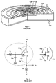
- a conventional silicon-based PIN diode detector differs from a conventional silicon-based PIN diode detector in that it has a field electrode arrangement comprising the so-called drift rings 101 and an amplifier integrated with the diode component.
- the amplifier is most typically a FET (Field-Effect Transistor), the source, gate and drain electrodes appear in fig. 1 as 102, 103 and 104 respectively.
- the anode and cathode of the detector diode are illustrated as 105 and 106 respectively in fig. 1.
- Fig. 2 illustrates schematically the elecrical operating principle of an SDD according to fig. 1.
- the dashed elliptical line illustrates, which part of the circuit diagram are located directly within the detector chip.
- An X-ray photon that hits the detector generates a cloud of free charge carriers, the size of the cloud - and correspondingly the total electric charge it contains - being dependent on the incident energy of the photon.
- the internal electric field of the detector causes the free charge carriers to drift towards the anode and cathode electrodes.
- the electric charge represented by the electrons arriving at the anode A can be thought of as a current pulse iq.
- the detector capacitance acts as an integrator that collects the current pulses and integrates them into an accumulating voltage.
- Said detector capacitance consists mainly of the anode capacitance Ca, but necessitates also considering the stray capacitances of the FET.
- the ionization rate which is a major factor controlling the flow of the leakage current I L , depends strongly on the voltage Vdg across the drain-gate junction of the FET. We may deduce that the value of the leakage current I L depends at least partly on the drain-source voltage Vds of the FET in the SDD.
- a detector appliance utilizing the detector described above with reference to figs. 1 and 2 comprises a voltage-sensitive measurement arrangement (not shown in fig. 2) adapted to measure changes in the potential designated as Vs .
- a problem of conventional SDD-based detector appliances is the rate dependent shift in peak positions.
- the rate at which X-ray photons hit the detector increases, also the voltage Vds increases. This would not be a problem as such, but becomes one because the detector capacitance is not constant but depends on voltages within the detector chip.
- a change in the detector capacitance Cdet means a change in the charge-to-voltage conversion factor of the detector.
- a peak representing radiation at a certain constant energy will shift to different locations depending on whether X-ray photons of that energy arrived at a slower or a faster rate. Whether the shift is upwards or downwards depends on the mutual order of relevance of the capacitances Ca and Cdg, because these have oppositely directed dependencies on the photon hit rate.
- a drift-type detector chip 301 comprises a FET 302, the source of which is coupled to a signal output through a preamplifier coupling 303.
- a current generator 304 adapted to draw a constant current through the FET; as noted above, since this current is essentially the same as the drain current, it is conventional to designate the current drawn by the current generator 304 as the drain current Id , although the coupling is to the source electrode of the FET.
- a differential amplifier 305 is coupled to measure the drain-to-source voltage Vds across the FET 302 and to give an output proportional thereto.
- a controlling amplifier 306 is adapted to compare the output of the differential amplifier 305 to a fixed reference voltage Vref and to use the comparison result to change the voltage produced by a controllable voltage source 308. The amplification and polarity of the controlling amplifier 306 have been carefully tuned so that the resulting change in Vd compensates for the rate-induced change in the charge-to-voltage conversion factor. Since the change of the charge-to-voltage conversion factor is nonlinear, a linearization circuit 307 is needed between the controlling amplifier 306 and the controllable voltage source 308.
- the circuit of fig. 3 involves problems that mainly relate to its susceptibility to oscillations.
- the most critical part is the differential amplifier 305, the input of which must be very well balanced on the operational frequencies of the control loop. It may also prove to be difficult to realize the linearization circuit 307, because of the complexity of the nonlinear behaviour of the charge-to-voltage conversion factor.
- the circuit may also be somewhat slow to react to changes in the photon hit rate.
- An objective of the present invention is to compensate for the rate dependent change of charge-to-voltage conversion factor in a drift-type radiation detector. Especially an objective of the invention is to realize such compensation in a manner that is simple to implement and realiable in operation. Additionally an objective of the invention is to provide a detector appliance that is adapted to compensate for rate dependent shift of the peak positions resulting from said .
- the objectives of the invention are achieved by changing the drain current as a function of momentary photon rate.
- a circuit arrangement according to the invention is characterised by the features recited in the characterising part of the independent claim directed to a circuit arrangement.
- the invention applies also to a detector appliance, which is characterised by the features recited in the characterising part of the independent claim directed to a detector appliance.
- the invention applies to a method for compensating for the rate dependent change of charge-to-voltage conversion factor in a drift-type radiation detector.
- the method is characterised by the features recited in the characterising part of the independent claim directed to a method.
- a controllable current generator (current source or current sink; more generally: a controllable circuit member adapted to cause a current of predefined magnitude to flow in response to a control signal) is used to controllably change the drain current as a function of photon hit rate, or as a function of the drain-to-source voltage of the FET in the detector chip, which as such is a function of the photon hit rate.
- I L Id ⁇ ⁇ ⁇ Vds ⁇ e ⁇ ⁇ Vds
- ⁇ and ⁇ are material- and temperature dependent constants.
- This expression is illustrative in two ways. Firstly, it confirms the statement made above about the complicated nonlinear relationship between I L and Vds, which makes it difficult to achieve satisfactory results by tampering with the value of Vds, which we attempted in fig. 3.
- expression (3) shows that the dependency between I L and Id is much simpler, even linear. We may thus deduce that it is possible to compensate for a purely rate dependent distortion of I L by causing a comparable distortion to Id, so that as a result Vds assumes the value it would have without said rate dependent distortion of I L .
- Fig. 4 illustrates schematically an arrangement in which a drift type detector chip 301 is used for detecting radiation.
- a FET 302 on the drift type detector chip 301 has its drain coupled to a first potential V1 .
- the source of the FET 302 is coupled to a second potential V2 through a controllable current generator 401.
- measurement circuitry 400 which may comprise amplifiers, pulse shaping circuits and a multichannel analyser (not separately shown in fig. 4).
- the arrangement of fig. 4 comprises a circuit element 402 adapted to collect information that describes the momentary rate at which photons hit the detector chip 301.
- the circuit element 402 produces an output signal the value of which represents a momentary value of the photon hit rate.
- the arrangement of fig. 4 comprises a circuit element 403 adapted to receive said output signal and to adjust the controllable current generator 401 so that the value of ld is changed by an amount that corresponds to an estimated rate dependent change in the value of the neutralization current I L .
- Circuit elements 402 and 403 can be implemented using analog or digital technology, or both.
- a feature typical to especially analog electronics is that a component or a circuit element may have multiple functions, and that it is not always possible to clearly separate a circuit arrangement into well-defined, separate functional blocks.
- the division into circuit elements 402 and 403 should therefore be considered merely as an illustrative aid in understanding the operation of certain embodiments of the invention, rather than any strict requirement to be fulfilled in practical implementations.
- the principle illustrated in fig. 4 does not restrict the selection of the source of the information collected by circuit element 402, as long as the selected source is capable of delivering accurate, up-to-date information describing the momentary photon hit rate.
- such information may be available from the drain side of the FET 302 according to arrow 411, from the source side of the FET 302 according to arrow 412, and/or even from the measurement circuitry 400 according to arrow 413.
- the middle alternative of these in more detail.
- Fig. 5 is a simplified schematic diagram illustrating a circuit arrangement where an SDD chip 301 is used to detect radiation.
- the FET 302 of the SDD chip 301 has its drain collected to a fixed voltage source 501 adapted to deliver a fixed drain voltage Vd.
- the source of the FET 302 is coupled to the input of a preamplifier 502, the output of which constitutes a signal output meant to be coupled to further measurement and storage circuitry.
- the source of the FET 302 is likewise coupled to one input of a differential amplifier 503, the other input of which is coupled to a fixed reference voltage Vref .
- the output of the differential amplifier 503 is coupled to a linearization circuit 504, from which there is a coupling to a control input of a controllable current generator 401.
- Said controllable current generator 401 is adapted to draw a current of controllable magnitude from the source of the FET 302 to ground.
- Vd Since the value of Vd is constant, all changes of Vds of the FET 302 appear directly in the source potential, which the differential amplifier 503 compares to the reference Vref .
- the value of Vref has been selected so that at a certain predefined photon hit rate at the SDD chip 301 there occurs a certain desired nominal drain current Id . Lower photon hit rates cause the drain current Id to decrease, and higher photon hit rates cause the drain current Id to increase, the relative amount of decreasing and increasing being basically dependent only on the amplification factor of the differential amplifier 503.
- the charge-to-voltage conversion factor of the SDD chip 301 would only remain constant if the gate voltage of the FET 302 remained constant.
- changes in Id imply changes also in the gate-to-source voltage Vgs of the FET 302, which means that the source potential monitored by the differential amplifier 503 is strictly speaking not an exact indicator of the drain-to-gate voltage Vdg of the FET 302, and thus neither of the charge-to-voltage conversion factor.
- the task of the linearization circuit 504 is to counteract the distortion that would otherwise result from said slight discrepancy between the source potential and the drain-to-gate voltage Vdg of the FET 302. Also careful tuning of the differential amplifier 503 helps to reduce said distortion.
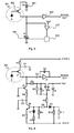
- Fig. 6 illustrates an exemplary detailed implementation of a circuit arrangement according to fig. 5.
- the drain of the FET J1 in the SDD chip 301 is coupled to a fixed +12V voltage through a resistor R1. Additionally there is an AC attenuator coupling from the drain of the FET J1 to ground through a capacitor C1.
- a coupling from the source of the FET J1 to the signal output goes through a conventional preamplifier arrangement consisting of the amplifier J2 and the associated capacitors C2 and C3.
- the controllable current path from the source of the FET J1 goes to the drain of another FET J3, continues from the source of said FET J3 through resistor R4 to the collector of an NPN transistor J5 and extends from the emitter of said NPN transistor J5 through resistor R7 to a fixed -15V voltage.
- the gate of FET J3 is coupled to ground; from the collector of the NPN transistor J5 is also coupled to ground through capacitor C6.
- the monitoring differential amplifier J4 receives a sample of the source potential of the FET J1 to its negative input through resistor R2. For tuning the differential amplifier J4 there are resistor R3 and capacitor C4 coupled in parallel between its negative input and its output.
- the reference voltage Vref is coupled to the positive input of the differential amplifier J4.
- An AC attenuator capacitor C5 couples the positive input of the differential amplifier J4 to ground.
- the output of the differential amplifier is coupled to the base of the NPN transistor J5 through resistors R5 and R6.
- the base of the NPN transistor J5 is also coupled to ground through resistor R9 and to the anode of a diode D1, from the cathode of which there is a coupling through resistor R8 to the fixed -15V voltage.
- the point between resistors R5 and R6 is coupled to the anode of diode D2, the cathode of which is coupled to ground through resistor R11 and to the fixed -15V voltage through resistor R10.
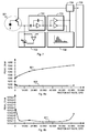
- Fig. 7 illustrates a detector appliance for measuring X-ray spectra. It comprises an SDD detector chip 301, an output of which is coupled to a preamplifier 701 and a compensation circuit 702 adapted to controllably change the value of a drain current drawn through an integrated FET of the SDD detector chip 301.
- the couplings of the SDD detector chip 301, the preamplifier 701 and the compensation circuit 702 are e.g. similar to those described above with reference to fig. 6.
- An output of the preamplifier 701 is coupled to a linear amplifier 703 comprising a measurement channel and a timing channel, each of which produces an output of its own. These outputs are coupled to a multichannel analyser 704.
- the detector appliance comprises also a platform functionality 705, which is adapted to produce and distribute operating voltages and to provide other kinds of support functions to the other functional blocks of the detector appliance.
- platform functionality 705 which is adapted to produce and distribute operating voltages and to provide other kinds of support functions to the other functional blocks of the detector appliance.
- the detector appliance comprises a circuit 706 adapted to respond to the output of the timing channel in the linear amplifier by controllably altering the charge neutralising effect of the drain voltage delivered to the SDD chip 301.
- Said circuit 706 can be e.g. of the kind described in detail in a co-pending US patent application no. 10/881420, which is incorporated herein by reference. It should be noted, however, that the arrangement disclosed in said co-pending US patent application also inherently counteracts the rate-dependent shift in the locations of spectral peaks, so combining it with the present invention might lead to certain redundancy in correction circuitry.
- FIG. 8a illustrates the observed peak position on the channels of the multichannel analyser when the compensation circuit was switched off, and the drain current was consequently constant.
- Graph 802 illustrates the observed peak position when the compensation circuit was in use.
- Graph 811 in fig. 8b is the same as graph 802 but in a more detailed scale. It is easy to note how a change in the photon hit rate from the order of a few hundred cps to 63 000 cps caused the peak position to shift by about 20 channel numbers when the compensation was not in use, while switching on the compensation enabled keeping the peak position within one half of a channel, and even essentially constant over a major part of the tested range of photon hit rates.
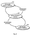
- FIG. 9 illustrates a method according to an embodiment in the form of a state diagram.
- a measurement state 901 corresponds to steady state conditions where the photon hit rate does not change and the charge-to-voltage conversion factor of the SDD detector chip and consequently the correspondence between photon energy and channel number in the multichannel analyser remains constant. If information is obtained about an increasing photon hit rate, the drain current drawn through the FET in the SDD chip is also increased in state 902 by a relative amount that is as close as possible to the increase in leakage current that was caused by the increasing photon hit rate. Correspondingly if there is obtained information about a decreasing photon hit rate, the drain current is decreased according to state 903.
Landscapes
- Engineering & Computer Science (AREA)
- Power Engineering (AREA)
- Measurement Of Radiation (AREA)
- Amplifiers (AREA)
- Light Receiving Elements (AREA)
Applications Claiming Priority (1)
| Application Number | Priority Date | Filing Date | Title |
|---|---|---|---|
| US10/971,208 US7193216B2 (en) | 2004-10-22 | 2004-10-22 | Method and circuit arrangement for compensating for rate dependent change of conversion factor in a drift-type radiation detector and a detector appliance |
Publications (1)
| Publication Number | Publication Date |
|---|---|
| EP1650871A1 true EP1650871A1 (fr) | 2006-04-26 |
Family
ID=35613691
Family Applications (1)
| Application Number | Title | Priority Date | Filing Date |
|---|---|---|---|
| EP05109703A Ceased EP1650871A1 (fr) | 2004-10-22 | 2005-10-19 | Procédé et appareil pour compenser des variations du facteur de conversion charge-tension dans un détecteur |
Country Status (3)
| Country | Link |
|---|---|
| US (1) | US7193216B2 (fr) |
| EP (1) | EP1650871A1 (fr) |
| JP (1) | JP4448484B2 (fr) |
Cited By (4)
| Publication number | Priority date | Publication date | Assignee | Title |
|---|---|---|---|---|
| US7339175B1 (en) | 2006-07-28 | 2008-03-04 | Thermo Electron Scientific Instruments Llc | Feedback circuit for output control in a semiconductor X-ray detector |
| EP2430432A4 (fr) * | 2009-05-15 | 2014-07-23 | Fei Co | Microscope électronique avec détecteur(s) intégré(s) |
| US9972474B2 (en) | 2016-07-31 | 2018-05-15 | Fei Company | Electron microscope with multiple types of integrated x-ray detectors arranged in an array |
| CN118519182A (zh) * | 2024-05-13 | 2024-08-20 | 湖南大学 | 基于nmos辐射总剂量的感应电路及光电编码器辐射补偿电路 |
Families Citing this family (12)
| Publication number | Priority date | Publication date | Assignee | Title |
|---|---|---|---|---|
| US7858946B2 (en) * | 2007-01-18 | 2010-12-28 | Bruker Ax Microanalysis Gmbh | Energy dispersive X-ray I-FET SDD detector appliance and a method for pulsed reset neutralization of accumulated charges within an energy dispersive X-ray I-FET SDD detector appliance |
| CN101281148B (zh) * | 2007-07-27 | 2011-01-05 | 江苏天瑞仪器股份有限公司 | 一种高分辨率的半导体核辐射探测器 |
| JP5606723B2 (ja) | 2008-12-25 | 2014-10-15 | 日本電子株式会社 | シリコンドリフト型x線検出器 |
| DE102011006154A1 (de) | 2011-03-25 | 2012-08-09 | Siemens Aktiengesellschaft | Verfahren zur Korrektur von Detektordaten eines Röntgendetektors und Röntgenaufnahmesystem |
| GB2491111B (en) * | 2011-05-19 | 2015-08-19 | Oxford Instr Nanotechnology Tools Ltd | Charge-sensitive amplifier |
| DE102011104489A1 (de) | 2011-06-17 | 2012-12-20 | Pndetector Gmbh | Halbleiterdriftdetektor und entsprechendes Betriebsverfahren |
| EP2544025A1 (fr) * | 2011-07-07 | 2013-01-09 | FEI Company | Détecteur au silicium à diffusion pour une utilisation dans un appareil de particules chargées |
| US9530902B2 (en) * | 2012-06-20 | 2016-12-27 | Oxford Instruments Analytical Oy | Two-dimensional guard structure and a radiation detector with the same |
| CN104407373B (zh) * | 2014-10-29 | 2017-01-18 | 中国科学院微电子研究所 | 辐射探测电路 |
| CN105044759B (zh) * | 2015-07-29 | 2018-01-23 | 中国船舶重工集团公司第七一九研究所 | 一种数字式核探测器的状态评估与保障维护方法及系统 |
| CN106525028B (zh) * | 2016-10-28 | 2019-05-24 | 北京控制工程研究所 | 用于x射线脉冲星导航敏感器的硅漂移探测器处理电路 |
| CN112071874B (zh) * | 2020-09-30 | 2024-06-14 | 湖南脉探芯半导体科技有限公司 | 一种硅漂移探测器与金属氧化物半导体场效应晶体管集成器件 |
Citations (2)
| Publication number | Priority date | Publication date | Assignee | Title |
|---|---|---|---|---|
| US3968361A (en) * | 1975-06-23 | 1976-07-06 | The United States Of America As Represented By The Secretary Of The Navy | Laser receiver anti-sun circuit |
| EP0301963A2 (fr) * | 1987-07-30 | 1989-02-01 | Societe Moderne D'electronique | Dispositif amplificateur de signaux de faible puissance, notamment issus d'une fibre optique plastique |
-
2004
- 2004-10-22 US US10/971,208 patent/US7193216B2/en not_active Expired - Fee Related
-
2005
- 2005-10-19 EP EP05109703A patent/EP1650871A1/fr not_active Ceased
- 2005-10-21 JP JP2005307572A patent/JP4448484B2/ja not_active Expired - Fee Related
Patent Citations (2)
| Publication number | Priority date | Publication date | Assignee | Title |
|---|---|---|---|---|
| US3968361A (en) * | 1975-06-23 | 1976-07-06 | The United States Of America As Represented By The Secretary Of The Navy | Laser receiver anti-sun circuit |
| EP0301963A2 (fr) * | 1987-07-30 | 1989-02-01 | Societe Moderne D'electronique | Dispositif amplificateur de signaux de faible puissance, notamment issus d'une fibre optique plastique |
Non-Patent Citations (6)
| Title |
|---|
| BERTUCCIO G ET AL.: "Silicon drift detector with integrated p-JFET for continuous discharge of collected electrons through the gate junction", NUCLEAR INSTRUMENTS AND METHODS IN PHYSICS RESEARCH A, vol. 377, 1996, pages 352 - 356 |
| BERTUCCIO G ET AL: "Silicon drift detector with integrated p-JFET for continuous discharge of collected electrons through the gate junction", NUCLEAR INSTRUMENTS & METHODS IN PHYSICS RESEARCH, SECTION - A: ACCELERATORS, SPECTROMETERS, DETECTORS AND ASSOCIATED EQUIPMENT, ELSEVIER, AMSTERDAM, NL, vol. 377, no. 2, 1 August 1996 (1996-08-01), pages 352 - 356, XP004008277, ISSN: 0168-9002 * |
| C. FIORINI; P. LECHNER: "Charge-sensitive preamplifier with continuous reset by means of the gate-to-drain current of the JFET integrated on the detector", IEEE TRANSACTIONS ON NUCLEAR SCIENCE, vol. 49, no. 3, June 2002 (2002-06-01), pages 1147 - 1151, XP002364505 * |
| CASTOLDI A ET AL: "Low-noise slew-rate free voltage preamplifier with current-limited continuous reset", NUCLEAR INSTRUMENTS & METHODS IN PHYSICS RESEARCH, SECTION - A: ACCELERATORS, SPECTROMETERS, DETECTORS AND ASSOCIATED EQUIPMENT, ELSEVIER, AMSTERDAM, NL, vol. 512, no. 1-2, 11 October 2003 (2003-10-11), pages 143 - 149, XP004468065, ISSN: 0168-9002 * |
| LABANTI C ET AL: "ICARUS-SDD: a 16 channel ASIC for silicon drift detectors read-out", NUCLEAR INSTRUMENTS & METHODS IN PHYSICS RESEARCH, SECTION - A: ACCELERATORS, SPECTROMETERS, DETECTORS AND ASSOCIATED EQUIPMENT, ELSEVIER, AMSTERDAM, NL, vol. 504, no. 1-3, 21 May 2003 (2003-05-21), pages 304 - 306, XP004426227, ISSN: 0168-9002 * |
| LECHNER P ET AL: "Silicon drift detectors for high resolution room temperature X-ray spectroscopy", NUCLEAR INSTRUMENTS & METHODS IN PHYSICS RESEARCH, SECTION - A: ACCELERATORS, SPECTROMETERS, DETECTORS AND ASSOCIATED EQUIPMENT, ELSEVIER, AMSTERDAM, NL, vol. 377, no. 2, 1 August 1996 (1996-08-01), pages 346 - 351, XP004008276, ISSN: 0168-9002 * |
Cited By (5)
| Publication number | Priority date | Publication date | Assignee | Title |
|---|---|---|---|---|
| US7339175B1 (en) | 2006-07-28 | 2008-03-04 | Thermo Electron Scientific Instruments Llc | Feedback circuit for output control in a semiconductor X-ray detector |
| EP2430432A4 (fr) * | 2009-05-15 | 2014-07-23 | Fei Co | Microscope électronique avec détecteur(s) intégré(s) |
| US8987665B2 (en) | 2009-05-15 | 2015-03-24 | Fei Company | Electron microscope with integrated detector(s) |
| US9972474B2 (en) | 2016-07-31 | 2018-05-15 | Fei Company | Electron microscope with multiple types of integrated x-ray detectors arranged in an array |
| CN118519182A (zh) * | 2024-05-13 | 2024-08-20 | 湖南大学 | 基于nmos辐射总剂量的感应电路及光电编码器辐射补偿电路 |
Also Published As
| Publication number | Publication date |
|---|---|
| JP4448484B2 (ja) | 2010-04-07 |
| JP2006119141A (ja) | 2006-05-11 |
| US7193216B2 (en) | 2007-03-20 |
| US20060086906A1 (en) | 2006-04-27 |
Similar Documents
| Publication | Publication Date | Title |
|---|---|---|
| US7193216B2 (en) | Method and circuit arrangement for compensating for rate dependent change of conversion factor in a drift-type radiation detector and a detector appliance | |
| Rehak et al. | Progress in semiconductor drift detectors | |
| De Geronimo et al. | Front-end electronics for imaging detectors | |
| US7547889B2 (en) | Photon detection device | |
| US8618457B2 (en) | Drive and measurement circuit for a photomultiplier | |
| US20100051818A1 (en) | Method and Apparatus for the Measurement of Signals from Radiation Sensors | |
| Niculae et al. | Optimized readout methods of silicon drift detectors for high-resolution X-ray spectroscopy | |
| Phipps et al. | A HEMT-based cryogenic charge amplifier with sub-100 eVee ionization resolution for massive semiconductor dark matter detectors | |
| Cardarelli et al. | Performance of RPCs and diamond detectors using a new very fast low noise preamplifier | |
| US20140332692A1 (en) | Semiconductor drift detector and corresponding operating method | |
| Fiorini et al. | Continuous charge restoration in semiconductor detectors by means of the gate-to-drain current of the integrated front-end JFET | |
| US7858946B2 (en) | Energy dispersive X-ray I-FET SDD detector appliance and a method for pulsed reset neutralization of accumulated charges within an energy dispersive X-ray I-FET SDD detector appliance | |
| CN116569072A (zh) | 用于光子计数应用的前端电子电路 | |
| KR102445626B1 (ko) | 포톤 검출기 | |
| US7271395B2 (en) | Device and method for the measurement of depth of interaction using co-planar electrodes | |
| Chase et al. | Amplifiers for use with pn junction radiation detectors | |
| CN103518140B (zh) | 用于测量电荷的系统 | |
| EP3758223B1 (fr) | Circuit de préamplificateur | |
| Fiorini et al. | Charge-sensitive preamplifier with continuous reset by means of the gate-to-drain current of the JFET integrated on the detector | |
| Fiorini et al. | A CMOS charge preamplifier for silicon drift detectors with on-chip JFET and feedback capacitor | |
| US20080290253A1 (en) | Image Sensor | |
| Dalla Betta et al. | JFET preamplifiers with different reset techniques on detector-grade high-resistivity silicon | |
| CN100484193C (zh) | 图像传感器 | |
| Fiorini et al. | A CMOS readout circuit for silicon drift detectors with on-clip JFET and feedback capacitor | |
| CN119519632B (zh) | 一种电荷放大器结构及其使用方法 |
Legal Events
| Date | Code | Title | Description |
|---|---|---|---|
| PUAI | Public reference made under article 153(3) epc to a published international application that has entered the european phase |
Free format text: ORIGINAL CODE: 0009012 |
|
| AK | Designated contracting states |
Kind code of ref document: A1 Designated state(s): AT BE BG CH CY CZ DE DK EE ES FI FR GB GR HU IE IS IT LI LT LU LV MC NL PL PT RO SE SI SK TR |
|
| AX | Request for extension of the european patent |
Extension state: AL BA HR MK YU |
|
| 17P | Request for examination filed |
Effective date: 20060623 |
|
| AKX | Designation fees paid |
Designated state(s): AT BE BG CH CY CZ DE DK EE ES FI FR GB GR HU IE IS IT LI LT LU LV MC NL PL PT RO SE SI SK TR |
|
| 17Q | First examination report despatched |
Effective date: 20110214 |
|
| STAA | Information on the status of an ep patent application or granted ep patent |
Free format text: STATUS: THE APPLICATION HAS BEEN REFUSED |
|
| 18R | Application refused |
Effective date: 20111121 |