EP1653149B1 - Ebene lichtquelle und deren verwendung in einer anzeigevorrichtung - Google Patents
Ebene lichtquelle und deren verwendung in einer anzeigevorrichtung Download PDFInfo
- Publication number
- EP1653149B1 EP1653149B1 EP04745882A EP04745882A EP1653149B1 EP 1653149 B1 EP1653149 B1 EP 1653149B1 EP 04745882 A EP04745882 A EP 04745882A EP 04745882 A EP04745882 A EP 04745882A EP 1653149 B1 EP1653149 B1 EP 1653149B1
- Authority
- EP
- European Patent Office
- Prior art keywords
- refractive element
- light
- light sources
- light source
- housing
- Prior art date
- Legal status (The legal status is an assumption and is not a legal conclusion. Google has not performed a legal analysis and makes no representation as to the accuracy of the status listed.)
- Expired - Lifetime
Links
Images




















Classifications
-
- G—PHYSICS
- G02—OPTICS
- G02B—OPTICAL ELEMENTS, SYSTEMS OR APPARATUS
- G02B6/00—Light guides; Structural details of arrangements comprising light guides and other optical elements, e.g. couplings
- G02B6/0001—Light guides; Structural details of arrangements comprising light guides and other optical elements, e.g. couplings specially adapted for lighting devices or systems
- G02B6/0011—Light guides; Structural details of arrangements comprising light guides and other optical elements, e.g. couplings specially adapted for lighting devices or systems the light guides being planar or of plate-like form
- G02B6/0013—Means for improving the coupling-in of light from the light source into the light guide
- G02B6/0023—Means for improving the coupling-in of light from the light source into the light guide provided by one optical element, or plurality thereof, placed between the light guide and the light source, or around the light source
- G02B6/0031—Reflecting element, sheet or layer
-
- G—PHYSICS
- G02—OPTICS
- G02B—OPTICAL ELEMENTS, SYSTEMS OR APPARATUS
- G02B6/00—Light guides; Structural details of arrangements comprising light guides and other optical elements, e.g. couplings
- G02B6/0001—Light guides; Structural details of arrangements comprising light guides and other optical elements, e.g. couplings specially adapted for lighting devices or systems
- G02B6/0011—Light guides; Structural details of arrangements comprising light guides and other optical elements, e.g. couplings specially adapted for lighting devices or systems the light guides being planar or of plate-like form
- G02B6/0033—Means for improving the coupling-out of light from the light guide
- G02B6/005—Means for improving the coupling-out of light from the light guide provided by one optical element, or plurality thereof, placed on the light output side of the light guide
- G02B6/0051—Diffusing sheet or layer
-
- G—PHYSICS
- G02—OPTICS
- G02B—OPTICAL ELEMENTS, SYSTEMS OR APPARATUS
- G02B6/00—Light guides; Structural details of arrangements comprising light guides and other optical elements, e.g. couplings
- G02B6/0001—Light guides; Structural details of arrangements comprising light guides and other optical elements, e.g. couplings specially adapted for lighting devices or systems
- G02B6/0096—Light guides; Structural details of arrangements comprising light guides and other optical elements, e.g. couplings specially adapted for lighting devices or systems the lights guides being of the hollow type
-
- G—PHYSICS
- G02—OPTICS
- G02F—OPTICAL DEVICES OR ARRANGEMENTS FOR THE CONTROL OF LIGHT BY MODIFICATION OF THE OPTICAL PROPERTIES OF THE MEDIA OF THE ELEMENTS INVOLVED THEREIN; NON-LINEAR OPTICS; FREQUENCY-CHANGING OF LIGHT; OPTICAL LOGIC ELEMENTS; OPTICAL ANALOGUE/DIGITAL CONVERTERS
- G02F1/00—Devices or arrangements for the control of the intensity, colour, phase, polarisation or direction of light arriving from an independent light source, e.g. switching, gating or modulating; Non-linear optics
- G02F1/01—Devices or arrangements for the control of the intensity, colour, phase, polarisation or direction of light arriving from an independent light source, e.g. switching, gating or modulating; Non-linear optics for the control of the intensity, phase, polarisation or colour
- G02F1/13—Devices or arrangements for the control of the intensity, colour, phase, polarisation or direction of light arriving from an independent light source, e.g. switching, gating or modulating; Non-linear optics for the control of the intensity, phase, polarisation or colour based on liquid crystals, e.g. single liquid crystal display cells
- G02F1/133—Constructional arrangements; Operation of liquid crystal cells; Circuit arrangements
- G02F1/1333—Constructional arrangements; Manufacturing methods
- G02F1/1335—Structural association of cells with optical devices, e.g. polarisers or reflectors
- G02F1/1336—Illuminating devices
- G02F1/133615—Edge-illuminating devices, i.e. illuminating from the side
-
- F—MECHANICAL ENGINEERING; LIGHTING; HEATING; WEAPONS; BLASTING
- F21—LIGHTING
- F21Y—INDEXING SCHEME ASSOCIATED WITH SUBCLASSES F21K, F21L, F21S and F21V, RELATING TO THE FORM OR THE KIND OF THE LIGHT SOURCES OR OF THE COLOUR OF THE LIGHT EMITTED
- F21Y2105/00—Planar light sources
- F21Y2105/10—Planar light sources comprising a two-dimensional [2D] array of point-like light-generating elements
-
- G—PHYSICS
- G02—OPTICS
- G02B—OPTICAL ELEMENTS, SYSTEMS OR APPARATUS
- G02B6/00—Light guides; Structural details of arrangements comprising light guides and other optical elements, e.g. couplings
- G02B6/0001—Light guides; Structural details of arrangements comprising light guides and other optical elements, e.g. couplings specially adapted for lighting devices or systems
- G02B6/0011—Light guides; Structural details of arrangements comprising light guides and other optical elements, e.g. couplings specially adapted for lighting devices or systems the light guides being planar or of plate-like form
- G02B6/0013—Means for improving the coupling-in of light from the light source into the light guide
- G02B6/0023—Means for improving the coupling-in of light from the light source into the light guide provided by one optical element, or plurality thereof, placed between the light guide and the light source, or around the light source
Definitions
- the portion of light radiated from a cold-cathode tube and light which is radiated from the cold-cathode tube and reflected on the cylindrical surface of a light source cover becomes parallel light with a focus lens and radiated on the reflection plane of a reflecting plate, and the reflected light is scattered from a scattering plate to be radiated (for example, refer to Japanese Unexamined Patent Publication No. 54625/1996 (page 3, line 18 of the left column to line 45 of the right column, Fig 2 )).
- JP 02-032320 discloses a back lighting device in which a pair of cylindrical light sources are provided near both sides in a lamp house, and a pair of convex lenses are placed so that each light source is positioned in a focal distance of the convex lens, respectively.
- a light reflecting plate is formed by bringing the inside surface of its own lamp house to specular processing. Accordingly, the surface of the light reflecting plate goes to completely specular, reflects a light beam emitted from the cylindrical light sources and the front display panel is brought to lighting.
- the object is attained by a planar light source according to claim 1 and a display device according to claim 8.
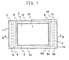
- the whole opening portion 1d of the housing 1 is provided with a scattering plate 2.
- the scattering plate 2 is a glass substrate or a resin plate such as polyethylene terephthalate (PET), acryl (PMMA) or polycarbonate (PC) which has a function of transmitting light. Further, those in which a reflecting material is mixed and those whose surface is roughened are used for the scattering plate 2 and a function for scattering irradiated light is imparted, thereby, it is preferable because the planar light source device having wide directivity can be obtained.
- PET polyethylene terephthalate
- PMMA acryl
- PC polycarbonate
- a plurality of point light sources 3 are provided by being arranged in the longitudinal direction of the substrate 4 of the point light sources on the rectangular substrate 4 of the point light sources.
- the substrate 4 of the point light sources is provided in parallel along two facing side planes 1c of the housing 1 and the plurality of point light sources 3 are provided in parallel along the side planes 1c of the housing 1.
- the reflecting plate 5 consists of a material which is obtained by depositing a metal such as aluminum or silver on a metal plate of such as aluminum or silver or a resin sheet. Further, the reflecting plate 5 is a regularly reflecting material which has a function of regularly reflecting light, and propagates light from the light source to a counter light source side by repeating reflection in which an incident angle coincides with a reflection angle on the reflecting plane of the reflecting plate 5.
- the reflection coefficient of the reflecting plate 5 and the reflector 7 is preferably 90 % or more in order to suppress reflection loss on the reflecting plane. Further, when the reflection coefficient is enhanced by making the inside of the housing 1 white, reflection in the inside is further improved and it is preferable because light loss is lessened. Further, although the reflecting plate 5 and the reflector 7 are composed of separate members, the number of members is lessened by integrally forming the reflecting plate 5 and the reflector 7 with the same member to be able to improve the workability of assembling. Further, when the housing 1 is designed to meet with the functions of the reflecting plate 5 and the reflector 7, it is preferable because the number of members can be reduced.
- the refractive element 8 in Example 1 has a bottom face 8a which is nearly parallel to the bottom face 1b side of the housing 1, the irradiated plane 8c which forms a slant angle at the reverse side from first cristas 8b to the bottom face 1b side of the housing 1 against the parallel bottom face 8a which passes the first cristas 8b of the bottom face 8a parallel to the point light sources 3 side, radiating plane 8e which forms a predetermined slant angle at the reverse side from the second cristas 8d to the bottom face 1b side of the housing 1 against the parallel bottom face 8a which passes the second cristas 8d of the bottom face parallel to the hollow space 6, and a facing face 8f which faces in parallel to the bottom face 8a.
- the refractive element 8 is a trapezoidal section shape in which thickness is increased from the top face 1a to the bottom face 1b of the housing 1, and formed by a transparent resin such as acryl or glass.
- the bottom face 8a of the refractive element 8 is arranged in nearly parallel to the bottom face 1b side of the housing 1, but it is not limited to this arrangement so far as light with an incident angle at which luminance is the maximum among light distribution of irradiating light for the irradiated plane 8c of the refractive element 8 is refracted to the bottom face 1b of the housing 1.
- it may be arranged in nearly parallel to the scattering plate 2 or the reflecting plate 5 or the like.
- liquid crystal display elements which apply the birefringence of liquid crystal, printed articles on which characters and pictures are printed on a transparent plate, and the like are mentioned, but the liquid crystal display elements are used as the display portion in Example 1.
- the liquid crystal display device is composed by including a circuit substrate not illustrated which drives the liquid crystal display elements and arranging the liquid crystal display elements on the upper portion of the planar light source device.
- the light path by which light emitted from the point light sources 3 is radiated from the scattering plate 2 is illustrated.
- Monochromatic lights of red, green and blue colors which are emitted from the first point light sources 3a, the second point light sources 3b and the third point light sources 3c being as the point light sources 3 are reflected directly or by a reflector 7 and irradiated on the irradiated plane 8c of the refractive element 8.
- light which is reflected on the surface of the irradiated plane 8c exists among lights which are irradiated from an oblique direction against the irradiated plane 8c of the refractive element 8. Since the light which is reflected on the surface of the irradiated plane 8c is reflected to the reflector 7 side and propagated in space which is surrounded by the reflector 7 and the refractive element 8, the light spreads in the longitudinal direction of the refractive element 8.
- the refractive index of the refractive element 8 is referred to as n (n is larger than the refractive index 1 of air), the slant angle of the irradiated plane 8c of the refractive element 8 is referred to as ⁇ 1 (0 ⁇ ⁇ 1 ⁇ 90°) and the slant angle of the radiating plane 8e of the refractive element 8 is referred to as ⁇ 2 (0 ⁇ ⁇ 2 ⁇ 90°).
- LEDs being the point light sources 3 control the directivity of the radiating light by sealing LED elements with a lens shaped resin.
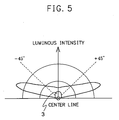
- a lens shaped resin For example, as shown in Fig. 5 , when right rotation from an upper side perpendicular to the central axis of arrangement direction of the LED elements is referred to as positive and LEDs which have the light distribution in which luminance is the maximum when the angle of the radiating lights from LEDs is at ⁇ 80° are used as the point light sources 3, an incident angle ⁇ i at which luminance is the maximum among light distribution of irradiating lights for the irradiated plane 8c of the refractive element 8 is 10° when the irradiated plane 8c of the refractive element 8 is nearly vertical to the bottom face 1b side of the housing 1, namely, the slant angle ⁇ 1 of the irradiated plane 8c of the refractive element 8 is 90°.
- the slant angle ⁇ 2 of the radiating plane 8e of the refractive element 8 satisfies ⁇ 2 ⁇ 70.05° from the inequality (3); therefore the bright portion nearby the light source is reduced and the distribution of luminance can be improved.
- the light which is irradiated on the scattering plate 2 is divided into the component of light transmitting in the scattering plate 2 and the component of light which is reflected by particles in the scattering plate 2.
- the component of light which is reflected to the bottom face 1b side of the housing 1 is normally reflected on the reflecting plate 5 and irradiated again on the scattering plate 2.
- the component of light which is irradiated on the scattering plate 2 and transmitted is radiated to all directions.
- the incident angle at which luminance is the maximum among light distribution of irradiating lights for the irradiated plane 8c of the direct light coincides with the incident angle at which luminance is the maximum among light distribution of irradiating lights for the irradiated plane 8c of the indirect light.
- the reflecting plate 5 which is nearly parallel to the bottom face 1b of the housing 1 or the scattering plate 2 is used, but as shown in Fig. 9 , the reflecting plate 5 may have first slant portions 5a in which a gap between the scattering plate 2 and the reflecting plate 5 is increased from the facing refractive element 8 to the center of the opening portion 1d of the housing 1.
- the incident angle of light at the first slant portions 5a is enlarged in comparison with an incident angle at the reflecting plate which is nearly parallel to the bottom face 1b of the housing 1 or the scattering plate 2, and light which is reflected by the reflecting plate can be reflected far from the light source.
- FIG. 9 is a partial section view of another planar light source device related to Example 1 which has first slant portions at a reflecting plate.
- Fig. 10 is an illustration view for illustrating the relation of distances between the first slant portions and the refractive element.
- Fig. 11 is an illustration view showing the ratio of luminance of the central portion of a display surface to the peripheral portion of the display surface against the distances x of a flat portion.
- the scattering reflection portion 9 can disarrange the propagation direction of light by scattering light which is irradiated on the scattering reflection portion 9, and can reflect it to the scattering plate 2 side.
- the scattering reflection portion 9 is situated at the center of the bottom face 1b of the housing 1, the luminance of the central portion of display can be preferably enhanced.
- the reflection coefficient of the scattering reflection portion is preferably 90 % or more for suppressing reflection loss at the reflection plane.
- the effective display zone 17 is a zone in which light from the planar light source device among the display portion which is not illustrated is irradiated, and is a display zone which comprises a plurality of pixels arranged in a matrix shape in the case of the liquid crystal display elements.
- Fig. 23 is a partial section view of another planar light source device related to Example 1 in which the edge of a reflector is extended to an effective display zone, according to the invention as claimed.
- the second reflectors 16 is formed in such a manner that its reflection plane is slanted to the hollow space 6 side from the top face 7a of the reflector 7 to the top face 1a of the housing 1, the light from the hollow space 6 side can be reflected on the bottom face 1b side of the housing 1, the radiating light from the scattering plate 2 nearby the light source is reduced, and the bright portion nearby the light source can be preferably improved.
- the refractive element 8 is a trapezoidal shape in which the lower side of the section of the refractive element 8 is longer than the upper side, for example, as shown in Fig. 17A , and the irradiated plane and the radiating plane are an oblique shape together; therefore surface reflection on the irradiated plane is increased, the radiating light from the scattering plate 2 nearby the light source is reduced, and the bright portion nearby the light source and the unevenness of colors can be reduced.
- the irradiated plane is slanted to a right side against the lower side and surface reflection on the irradiated plane is increased; therefore the unevenness of luminance and the unevenness of chromaticity of the radiating light from the refractive element 8 in the arrangement direction of the point light sources 3 can be further reduced.
- the refractive element 8 is a trapezoidal shape in which the lower side of the section of the refractive element 8 is longer than the upper side, the irradiated plane is slanted and the radiating plane is a shape vertical to the lower side; therefore surface reflection on the irradiated plane is increased, the radiating light from the scattering plate 2 nearby the light source is reduced, and the bright portion nearby the light source and the unevenness of colors can be reduced.
- the irradiated plane is slanted to a right side against the lower side and the surface reflection on the irradiated plane is increased; therefore the unevenness of luminance and the unevenness of chromaticity of the radiating light from the refractive element 8 in the arrangement direction of the point light sources 3 can be further reduced.
- an incident angle for the irradiated plane is large in comparison with a case that the irradiated plane is slanted against the lower side, and total reflection on the irradiated plane occurs easily. Thereby, the radiating light from the scattering plate nearby the light source is reduced, and the bright portion nearby the light source and the unevenness of colors can be reduced.
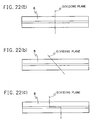
- FIG. 22B is an illustration view for illustrating a case of dividing the refractive element with a plane oblique to the direction of length hand of the refractive element shown in Fig. 17A
- Fig. 22C is an illustration view for illustrating a case of dividing so that the section of the direction of length hand of the refractive element shown in Fig. 17A is formed with a plurality of planes.
- the point light sources 3 are provided on the bottom face 1b of the housing 1 along the side face 1c side of the housing 1, but they are not limited to this arrangement.
- they may be provided at the side face 1c side of the housing 1.
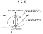
- the point light sources 3 has light distribution property that the light distribution to a direction providing the point light sources 3 is broad and directivity is a direction vertical to a direction providing the point light sources 3 and high in the central axis of LED. Since the light distribution of the point light sources 3 to a provision direction is broad, the unevenness of luminance and the unevenness of chromaticity caused by the studded point light sources 3 can be reduced.
- Fig. 24 is a partial section view of another planar light source device related to Example 1 in which the point light sources are provided at the side face of the housing.
- Fig. 25 is a chart showing the light distribution of radiating light from another LED which is used as the point light sources related to Example 1 of the present invention.
- the refractive element 8 which is extended to the arrangement direction of the plurality of point light sources 3 between the point light sources 3 and the hollow space 6 refracts light with an incident angle at which luminance is the maximum among light distribution of irradiating light for the irradiated plane of the refractive element 8, to the bottom face 1b side of the housing 1.
- Example 1 since it is composed of the refractive element 8 being a single prism as Fig. 2 , the thickness of the refractive element 8 is thickened when a small oblique angle ⁇ 2 is required, and miniaturization and weight saving are difficult.
- Example 2 as shown in Fig. 26 , since the refractive element 11 is a composition having a prism array in which a lot of prisms are repeatedly arranged, the refractive element 11 can be thinned, and miniaturization and weight saving can be achieved as a device.
- the refractive element 11 can independently control the direction of the radiating light against the irradiating light at the top face 1a side and the irradiating light at the bottom face 1b side by arranging a shape in which the oblique angle ⁇ 2 of the radiating plane is gradually enlarged from the top face 1a to the bottom face 1b of the housing 1; therefore the radiating light can be more accurately controlled.
- the shape of the refractive element is selected by the directivity of the point light sources and a refractive index ratio of the refractive element to a peripheral medium surrounding the refractive element.
- Fig. 28 is a partial section view of a planar light source device related to Example 3
- Figs. 29 A and 29B are evolution charts showing the refractive element related to Example 3
- Fig. 29A is a top view viewed from the top face side of the housing
- Fig. 29B is a frontal view viewed from the hollow space side.
- Fig. 30 is an illustration view showing a light path possibly occurring when light transmitting in the refractive element is totally reflected on a radiating plane.
- the same numerals as Figs. 1 to 27C show the same portions or equivalent portions, and their illustration is abbreviated.
- the refractive element 12 has the bottom face 12a which is nearly parallel to the bottom face 1b of the housing 1 or the scattering plate 2, the irradiated plane 12c which forms a fixed oblique angle ⁇ 1 at the reverse side from the first crista 12b to the bottom face 1b side of the housing 1 against the bottom face 12a which passes the first crista 12b of the bottom face 12a to the point light sources 3 side, a plurality of faces 12g which are parallel to the bottom face 12a, the radiating plane 12e which forms a fixed oblique angle ⁇ 2 at the reverse side from the cristas 12d to the bottom face 1b side of the housing 1 against the parallel bottom faces 12g which pass the respective cristas 12d of a plurality of parallel planes 12g, and the facing planes 12f which face the bottom face 12a in parallel.
- the irradiated plane 12c of the refractive element 12 has concave portions 12h which are extended to the thickness direction of the housing 1.
- the concave portions 12h are composed by combining 2 planes, and the convex portions with an apex angle ⁇ 3 (0° ⁇ ⁇ 3 ⁇ 180°) are formed by the adjacent concave portions 12h.
- Example 3 is different from Example 1 and 2 only in a point that the refractive element 12 has the concave portions 12h which are extended to the thickness direction of the housing 1. It exhibits a similar action effect as Example 1 and 2 other than the action effect according to the concave portions 12h of the refractive element 12 described later.
- the refractive index of the refractive element 12 is set as n (n is larger than the refractive index 1 of air)
- an apex angle which is formed by the adjacent concave portions 12h of the refractive element 12 is set as ⁇ 3 (0° ⁇ ⁇ 3 ⁇ 180°) and an incident angle from the point light sources 3 to the irradiated plane 12c of the refractive element 12 is set as ⁇ 2 (-90° ⁇ ⁇ 2 ⁇ 90°)
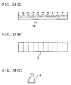
- Figs. 31A to 31C are evolution charts showing another refractive element related to Example 3, Fig. 31A is a top view viewed from the top face side of the housing, Fig. 31B is a frontal view viewed from the hollow space side, and Fig. 31C is a side view viewed from the longitudinal direction of the refractive element.
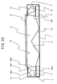
- Fig. 32 is a section view of a planar light source device related to Example 4.
- Figs. 33A and 33B are illustration views for illustrating action of the refractive element
- Fig. 33A is a magnified view nearby the refractive element related to Example 4
- Fig. 33B is a magnified view nearby the refractive element of Fig. 17A .
- the same numerals as Figs. 1 to 31C show the same portions or equivalent portions, and their illustration is abbreviated.
- the bottom faces 48a of the refractive element 48 are rough surfaces as an optical scattering means, but the present invention is not limited to this arrangement.
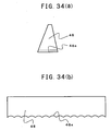
- Figs. 34A and 34B the broadening of light reflected on the bottom faces 48a to the direction of length hand of the refractive element can be selectively controlled by forming grooves which are extended to a horizontal direction of the refractive element 48 on the bottom faces 48a of the refractive element 48. Consequently, the unevenness of luminance and the unevenness of colors originated in that the point light sources 3 are discretely arranged can be also improved.
- Fig. 34A is a section view of refractive element related to Example 4
- Fig. 34B is a frontal view viewed from the hollow space side of another refractive element related to Example 4.
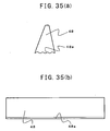
- Figs. 35A and 35B the broadening of light reflected on the bottom faces 48a to the horizontal direction of the refractive element can be selectively controlled by forming grooves which are extended to the longitudinal direction of the bottom faces 48a of the refractive element 48. Consequently, it can be mitigated that luminance is heightened nearby the point light sources 3 and the unevenness of luminance can be improved.
- Fig. 35A is a section view of refractive element and Fig. 35B is a frontal view viewed from the hollow space side of refractive element.
- Example 4 the unevenness of luminance and the unevenness of colors nearby light injection are improved by providing the light scattering means on the bottom faces 48a of the refractive element 48, but in the present invention, the shape of the refractive element is not limited to this arrangement, and the unevenness of luminance and the unevenness of colors of the radiating light from the scattering plate 2 can be further improved by the effect shown in Example 1 to 3 and the effect of Example 4, by providing the light scattering means on the bottom faces of the refractive element having shapes which are shown in Examples 1 to 3.
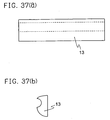
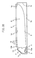
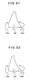
- the irradiated plane 13a is a semispherical shape which surrounds LEDs matching with the lens shape of a resin sealing the LED elements so that lights to all directions from LEDs being the point light sources 3 are irradiated nearly perpendicular to the irradiated plane 13a. Thereby, an incident angle at the irradiated plane 13a can be reduced (vertical incidence), and light irradiated on the irradiated plane 13a can be efficiently irradiated on the curved surfaces 13d or the radiating plane 13b.
- Fig. 39 is a section view of a planar light source device related to Example 6 and Figs. 40A and 40B are views for illustrating the action effect of the refractive element.
- Fig. 40A is a magnified view nearby the refractive element related to Example 6, and
- Fig. 40B is a magnified view nearby the refractive element of Fig. 17A .
- the same numerals as Figs. 1 to 38 show the same portions or equivalent portions which are shown in Figs. 1 to 38 , and their illustration is abbreviated. It is only different from the Example 1 that Example 6 has a characteristic in the shape of the refractive element 8 described later, and it exhibits the similar action effect as Example 1 other than the action effect according to the refractive element 8.
- the height of the first planes 8c1 in the present Example is illustrated using Fig. 41 .
- the left side of the page space is the point light sources 3 side
- the right side is the hollow space 6 side.
- the maximum light distribution angle of the point light sources 3 is about 90° as shown in Fig. 5
- light about parallel to the bottom face 8a is the light of the maximum light distribution angle.
- P a point in which light which is emitted from the point light sources 3, refracted on the second planes 8c2 and reaches the cristas 8d is irradiated on the second planes 8c2 is referred to as P.
- the first planes 8c1 may be provided at a range of the bottom face 8a side than the point P. Consequently, when the oblique angle of the second planes 8c2 is set as ⁇ , the refractive index of the refractive element 8 as n1, the width of the refractive element as w1 and the height of the first planes 8c1 as h1, the range may be a range satisfying the following formula (7). 0 ⁇ h ⁇ 1 ⁇ w ⁇ 1 / Tan ⁇ + Sin - 1 Sin 90 - ⁇ / n ⁇ 1
- the radiating plane 18e of the refractive element 18 can be formed by polygon.
- the radiating plane 18e of the refractive element 18 can be formed by a curved surface.
- the direction of light can be more accurately controlled by forming the radiating plane with polygon or a curved surface.
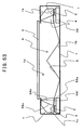
- the refractive element 28 comprises the irradiated plane 28c of the point light sources 3 side which comprises the first planes 28c1 nearly vertical to the bottom face 1b of the housing 1 and the second planes 28c2 which are linked with the first planes 28c1 and slanted to the hollow space 6 side, the first planes 28e1 in which the radiating plane 28e at the hollow space 6 side is slanted to the point light sources 3 side, and the second planes 28e2 which are linked with the first planes 28e1 and nearly vertical to the bottom face 1b of the housing 1. Further, it has the bottom faces 28a which is nearly parallel to the bottom face 1b of the housing 1 and the facing faces 28f which face in parallel to the bottom faces 28a.
- the refractive element 28 is prepared by transparent resin such as acryl or glass. Further, in Example 8, since the irradiated plane 28c and the radiating plane 28e are respectively formed only by two planes, processing is easy.
- the second planes 28c2 which are linked with the first planes 28c1 and slanted to the hollow space 6 side are provided as the irradiated plane 28c, light L1 which is surface-reflected among light reaching the second planes 28c2, returned to the reflector 7 side and is utilized again is increased. Consequently, the radiating light from the scattering plate 2 nearby the light source 3 is reduced, and the unevenness of luminance of the radiating light from the scattering plate 2 can be improved.
- the boundary line 28c3 between the first planes 28c1 and the second planes 28c2 of the irradiated plane 28c is situated at the bottom face 1b side in comparison with the boundary line 28e3 between the first planes 28e 1 and the second planes 28e2 of the radiating plane 28e.
- Fig. 53 is a section view of the planar light source device related to Example 9 and Figs. 54A and 54B are partial section views for illustrating the action effect of the refractive element.
- Fig. 54A is a magnified view nearby the refractive element related to Example 9
- Fig. 54B is a magnified view nearby the refractive element of Fig. 17A .
- Fig. 55 is a view for illustrating the shape of the refractive element.
- the same numerals as Figs. 1 to 52 show the same portions or equivalent portions which are shown in Figs. 1 to 52 , and their illustration is abbreviated. Only the shape of the refractive element 58 in Example 9 which is described later is different from Example 1, and it exhibits the similar action effect as Example 1 other than the action effect according to the refractive element 58.
- the angle ⁇ is reduced in accordance with that the incident angle ⁇ i is reduced by the inequality (13). Accordingly, when ⁇ is set so as to satisfy the inequality (13) in light in which the incident angle ⁇ i among radiating light from the point light sources 3 is smallest, namely light with the maximum light distribution angle, it is preferable because all of light reflected at the bottom faces 58a is radiated from the opening portion 1d side to the bottom face 1b side of the housing 1. For example, as shown in Fig.
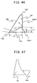
- the refractive element 38 in Example 10 has the bottom faces 38a which are provided along the arrangement direction of the plurality of point light sources 3 between the point light sources 3 and the hollow space 6 and nearly parallel to the bottom face 1b of the housing 1, the facing planes 38f which face in parallel to the bottom faces 38a, the irradiated plane 38c which is brought in contact with the bottom faces 38a and the facing planes 38f and are slanted to the hollow space 6 side, and the radiating plane 38e which is brought in contact with the bottom faces 38a and the facing planes 38f and is slanted to the point light sources 3 side. Further, a black sheet is pasted on the bottom faces 38a as the light absorbing member 39. Further, the refractive element 38 is prepared by transparent resin such as acryl or glass.
- a black sheet is used for the light absorbing member 39, but in the present invention, it is not limited to this arrangement, so far as it has a function of absorbing at least the portion of light.
- a gray sheet can be used.
- a gray color and a black color may be coated on the bottom face of the refractive element 38.
- Example 10 the radiating light from the scattering plate 2 nearby the light source 3 is suppressed and the unevenness of luminance of the radiating light from the scattering plate 2 is improved using the light absorbing member 39 on the bottom faces 38a of the refractive element 38, but the shape of the refractive element is not limited to this arrangement in the present invention, and the unevenness of luminance of the radiating light from the scattering plate 2 can be further improved by the effects shown Examples 1 to 9 and the effect of Example 10, by using the light absorbing member on the bottom faces of the refractive element having the shapes which are shown in, for example, Examples 1 to 9.
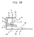
- Example 11 is different from Examples 1 to 4 only in a point that the refractive element is not provided in the planar light source device and the substrate 4 of the point light sources is slanted against the bottom face 1b of the housing 1 or the scattering plate 2 so that the planes 15 which are perpendicular to the central axis 14 of the point light sources 3 and the bottom face 1b of the housing 1 form an angle ⁇ . It exhibits the similar action effect as Example 1 to 4 other than the action effect according to the substrate 4 of the point light sources which is described later.
- the radiating light from the scattering plate 2 nearby the light source can be reduced by directing the light in which luminance is the maximum among light distribution of the radiating lights from the point light sources 3, to the bottom face 1b of the housing 1, namely, by slanting the substrate 4 of the point light sources so that the light in which luminance is the maximum is horizontal or less.
- the propagation distance of light in the hollow space 6 is increased, the color mixing and mixing of lights are accelerated, and it is preferable because the unevenness of luminance and the unevenness of chromaticity can be reduced.
- Fig. 59 there is illustrated below a case that the radiating light with an angle ⁇ 3 at which luminance is the maximum among light distribution of the radiating light from the point light sources 3 relative to the central axis 14 of the point light sources 3 is horizontal against the bottom face 1b of the housing 1.
- LEDs being the point light sources 3 control the directivity of the radiating light by sealing LED elements with a lens shaped resin.
- a lens shaped resin For example, as shown in Fig. 5 , when right rotation from an upper side perpendicular to the central axis of arrangement direction of the LED elements is referred to as positive and LEDs which have the light distribution in which luminance is the maximum when the angle of the radiating light from LEDs is at ⁇ 80° are used as the point light sources 3, the angle ⁇ 3 is 80°, and an angle ⁇ which is formed between the planes 15 which are perpendicular to the central axis 14 of the point light sources 3 and the bottom face 1b of the housing 1 can reduce the bright portion nearby the light source and improve the distribution of luminance by satisfying ⁇ ⁇ 10° by the inequality (16).
- the radiating light which is radiated from the position S 1 can be firstly reflected on the reflecting plate 5 at the center of the bottom face 1b of the housing 1 by satisfying the following formula (17), and it is preferable because the luminance at the center of a display surface can be heightened in comparison with the surrounding of the point light sources.
- Tan - 1 d 1 / L 1 ⁇ + ⁇ 3 - 90 ⁇ °
- the reflector 7 having a shape by which with respect to light which reaches directly from the point light sources 3 to the hollow space 6, an incident angle at which luminance is the maximum among light distribution of the irradiating light for a hypothetical plane being a boundary between the hollow space and a zone surrounded by the reflector 7 from the point light sources 3 coincides with an incident angle at which luminance is the maximum among light distribution of the irradiating light for a hypothetical plane being a boundary between the hollow space and a zone surrounded by the reflector 7, with respect to light which is reflected on the reflector 7 from the point light sources 3 and reaches to the hollow space 6.
- the radiating light in which luminance is the maximum among light distribution of the radiating light from the point light sources 3 for the central axis 14 of the point light sources 3 can be radiated to the bottom face 1b side of the housing 1 by satisfying the inequality (16); therefore luminance nearby the point light sources is not heightened in comparison with luminance at a position far from the point light sources and the unevenness of luminance at the display surface can be improved.
- planar light source device is not required to provide the refractive element, the reduction of the number of members and the reduction of member cost can be carried out.
- Example 12 is different from Example 11 only in a point that the substrate 4 of the point light sources is provided in the housing 1 so that the point light sources 3 are situated at the top face 1a side of the housing 1. It exhibits the similar action effect as Example 11 other than the action effect according to the substrate 4 of the point light sources which is described later.
- Example 12 since the point light sources 3 are situated at the top face 1a side of the housing 1, nearly all of radiating lights from the point light sources 3 can be radiated to the bottom face 1b side of the housing 1; therefore luminance nearby the point light sources is not heightened in comparison with luminance at a position far from the point light sources and the unevenness of luminance at the display surface can be suppressed.
- the radiating angle of the radiating light in which luminance is the maximum among light distribution of the radiating light from the point light sources 3 for the central axis 14 of the point light sources 3 is set as ⁇ 3 (-90° ⁇ ⁇ 3 ⁇ 0°)
- a horizontal distance until the center O 2 of the opening portion 1d of the housing 1 is set as L 2 based on a position S 2 at which the radiating light in which luminance is the maximum among light distribution of the radiating light from the point light sources 3 for the central axis 14 of the point light sources 3 is radiated
- a vertical distance from the center O 2 of the opening portion 1d of the housing 1 to the reflecting plate 5 which is arranged at the bottom face 1b side of the housing 1 is set as d 2 .
- the radiating light which is radiated from the position S 2 can be firstly reflected on the reflecting plate 5 at the center of the bottom face 1b of the housing 1 by satisfying the following formula (18), and it is preferable because the luminance at the center of a display surface can be heightened in comparison with the surrounding of the point light sources.
- Tan - 1 d 2 / L 2 90 ⁇ ° + ⁇ 3
- effects by respective members are obtained by individually using the refractive element with various shapes, the reflector, the scattering reflection portion, the reflection plate having the first slant portions or the second slant portions, or the scattering plate having a light shielding pattern, but further effects can be expected by combining a plurality of kind of members.
- the present invention has the refractive element which exists extendedly to the arrangement direction of a plurality of point light sources between the point light sources and the hollow space, and the refractive element can radiate a greater part of lights among radiating lights from the refractive element to the bottom face side of the housing by refracting light with an incident angle at which luminance is the maximum among light distribution of the irradiating light against the irradiated plane of the refractive element, to the bottom face side of the housing. Consequently, luminance nearby the point light sources is not heightened in comparison with luminance at a position far from the point light sources and the unevenness of luminance at the display surface can be improved.
Landscapes
- Physics & Mathematics (AREA)
- General Physics & Mathematics (AREA)
- Optics & Photonics (AREA)
- Nonlinear Science (AREA)
- Mathematical Physics (AREA)
- Chemical & Material Sciences (AREA)
- Crystallography & Structural Chemistry (AREA)
- Planar Illumination Modules (AREA)
- Liquid Crystal (AREA)
Claims (8)
- Planare Lichtquellenvorrichtung mit:einem Gehäuse (1) mit einem Öffnungsabschnitt (1d) an einer Deckfläche und mit einem hohlen Zwischenraum,einer Streuplatte (2), die an dem Öffnungsabschnitt angeordnet ist,einer Reflexionsplatte (5), die an dem Bodenabschnitt des hohlen Zwischenraums des Gehäuses angeordnet ist,einer Mehrzahl von Punktlichtquellen (3), die in Reihe entlang zumindest einer Seite des Gehäuses angeordnet sind,gekennzeichnet durchein Brechungselement (8), das parallel zu der Mehrzahl von Punktlichtquellen und zwischen der Mehrzahl von Punktlichtquellen und dem hohlen Zwischenraum angeordnet ist und von der Mehrzahl von Punktlichtquellen abgestrahltes Licht bricht,einen ersten Reflektor (7), der die Mehrzahl von Punktlichtquellen umgibt außer auf der Seite zu dem hohlen Zwischenraum,wobei eine Kante (7b) der Deckfläche (7a) des ersten Reflektors (7) sich in eine wirksame Anzeigezone (17) innerhalb des hohlen Zwischenraums erstreckt, undein zweiter Reflektor (16) an einer Lücke zwischen der Deckfläche (7a) des ersten Reflektors und der Deckfläche des Gehäuses angeordnet ist.
- Planare Lichtquellenvorrichtung gemäß Anspruch 1, bei der eine bestrahlte Ebene (8c) des Brechungselements (8) von der Grundfläche (1b) des Gehäuses (1) zu der Deckfläche (1a) des Gehäuses zu dem hohlen Zwischenraum hin geneigt ist.
- Planare Lichtquellenvorrichtung gemäß Anspruch 1, bei der:das Brechungselement (8) so angeordnet ist, dass Sin-1(n × Sin(180°-θ1-θ2-Sin-1((1/n) × Sinφi)))-(90°-θ2) ≥ 0° erfüllt ist, wobeiein Brechungsindex des Brechungselements als n bezeichnet ist (n > 1),ein Neigungswinkel der bestrahlten Ebenen des Brechungselements als θ1 bezeichnet ist (0 < θ1 ≤ 90°),ein Neigungswinkel der Abstrahlebenen des Brechungselements als θ2 bezeichnet ist (0 < θ2 ≤ 90°) undein Auftreffwinkel, in dem die Leuchtdichte in der Lichtverteilung des Einstrahlungslichts für die bestrahlte Ebene maximal ist, als φi bezeichnet ist (-90° < φi < 90°).
- Planare Lichtquellenvorrichtung gemäß Anspruch 1, bei der das Brechungselement (8) ein Mittel aufweist zum Ausbreiten des einfallenden Lichts in einer Längsrichtung des Brechungselements.
- Planare Lichtquellenvorrichtung gemäß Anspruch 1, bei der das Brechungselement (48) ein Lichtstreumittel (48a) an der Grundfläche aufweist.
- Planare Lichtquellenvorrichtung gemäß Anspruch 1, bei der die Reflexionsplatte einen ersten Schrägabschnitt (5a) aufweist, in dem eine Lücke zwischen der Streuplatte und der Reflexionsplatte von der Mehrzahl von Punktlichtquellen aus zu einer der Seite des hohlen Zwischenraum zugewandten Seitenebene hin zunimmt.
- Planare Lichtquellenvorrichtung gemäß Anspruch 1, bei der bei der die Reflexionsplatte (5) einen zweiten Schrägabschnitt (5b) aufweist, in dem eine Lücke zwischen der Streuplatte und der Reflexionsplatte von der Mehrzahl von Punktlichtquellen aus zu einer der Seite des hohlen Zwischenraum zugewandten Seitenebene hin abnimmt.
- Anzeigevorrichtung mit:der planaren Lichtquellenvorrichtung, wie sie in einem der Ansprüche 1 bis 7 angegeben ist, undeiner Anzeige, die auf der planaren Lichtquellenvorrichtung angeordnet ist.
Applications Claiming Priority (3)
| Application Number | Priority Date | Filing Date | Title |
|---|---|---|---|
| JP2003170443 | 2003-06-16 | ||
| JP2003352590 | 2003-10-10 | ||
| PCT/JP2004/008328 WO2004111532A1 (ja) | 2003-06-16 | 2004-06-14 | 面状光源装置および該装置を用いた表示装置 |
Publications (3)
| Publication Number | Publication Date |
|---|---|
| EP1653149A1 EP1653149A1 (de) | 2006-05-03 |
| EP1653149A4 EP1653149A4 (de) | 2006-06-14 |
| EP1653149B1 true EP1653149B1 (de) | 2011-10-19 |
Family
ID=33554421
Family Applications (1)
| Application Number | Title | Priority Date | Filing Date |
|---|---|---|---|
| EP04745882A Expired - Lifetime EP1653149B1 (de) | 2003-06-16 | 2004-06-14 | Ebene lichtquelle und deren verwendung in einer anzeigevorrichtung |
Country Status (6)
| Country | Link |
|---|---|
| US (2) | US7229198B2 (de) |
| EP (1) | EP1653149B1 (de) |
| JP (1) | JP4705470B2 (de) |
| KR (1) | KR100804653B1 (de) |
| TW (1) | TWI238372B (de) |
| WO (1) | WO2004111532A1 (de) |
Cited By (1)
| Publication number | Priority date | Publication date | Assignee | Title |
|---|---|---|---|---|
| US9869444B2 (en) | 2015-06-24 | 2018-01-16 | Hyundai Motor Company | Flat lamp structure |
Families Citing this family (123)
| Publication number | Priority date | Publication date | Assignee | Title |
|---|---|---|---|---|
| FR2875993B1 (fr) * | 2004-09-28 | 2006-12-08 | Thales Sa | Boite a lumiere a diodes electroluminescentes |
| US8430548B1 (en) * | 2004-11-17 | 2013-04-30 | Fusion Optix, Inc. | Enhanced light fixture with volumetric light scattering |
| US20060221610A1 (en) * | 2005-04-01 | 2006-10-05 | Chew Tong F | Light-emitting apparatus having a plurality of overlapping panels forming recesses from which light is emitted |
| JP4513759B2 (ja) * | 2005-04-27 | 2010-07-28 | 三菱電機株式会社 | 面状光源装置 |
| US20060291241A1 (en) * | 2005-06-22 | 2006-12-28 | Carmanah Technologies Corp. | Light emitting diode illuminated display panel assembly |
| JP4797161B2 (ja) * | 2005-07-27 | 2011-10-19 | 国立大学法人東北大学 | 液晶ディスプレイ用バックライトユニット |
| US7513669B2 (en) * | 2005-08-01 | 2009-04-07 | Avago Technologies General Ip (Singapore) Pte. Ltd. | Light source for LCD back-lit displays |
| US7815355B2 (en) | 2005-08-27 | 2010-10-19 | 3M Innovative Properties Company | Direct-lit backlight having light recycling cavity with concave transflector |
| US7537374B2 (en) * | 2005-08-27 | 2009-05-26 | 3M Innovative Properties Company | Edge-lit backlight having light recycling cavity with concave transflector |
| US7473019B2 (en) | 2005-09-29 | 2009-01-06 | Osram Opto Semiconductors Gmbh | Lighting apparatus |
| NL1030161C2 (nl) | 2005-10-11 | 2007-04-12 | Matthijs Dirk Meulenbelt | Presentatie-inrichting. |
| TW200728851A (en) * | 2006-01-20 | 2007-08-01 | Hon Hai Prec Ind Co Ltd | Backlight module |
| JP4966701B2 (ja) * | 2006-08-03 | 2012-07-04 | ハリソン東芝ライティング株式会社 | 中空式面照明装置 |
| EP2074655B1 (de) * | 2006-10-12 | 2016-04-13 | Panasonic Intellectual Property Management Co., Ltd. | Lichtemittierende vorrichtung |
| JP2008123973A (ja) * | 2006-11-16 | 2008-05-29 | Mitsubishi Electric Corp | 面状光源装置および液晶表示装置 |
| US7538340B2 (en) * | 2006-12-01 | 2009-05-26 | Avago Technologies Ecbu Ip (Singapore) Pte. Ltd. | Low side emitting light source and method of making the same |
| JP2008153057A (ja) * | 2006-12-18 | 2008-07-03 | Citizen Electronics Co Ltd | 光源ユニット、バックライトユニット及び表示装置 |
| JP4835936B2 (ja) * | 2007-01-12 | 2011-12-14 | ミネベア株式会社 | 面状照明装置 |
| KR20100021477A (ko) * | 2007-05-20 | 2010-02-24 | 쓰리엠 이노베이티브 프로퍼티즈 컴파니 | 컬러 led 광원을 효율적으로 이용하는 백색광 백라이트 등 |
| TWI448643B (zh) | 2007-05-20 | 2014-08-11 | 3M Innovative Properties Co | 背光與利用背光之顯示系統 |
| TWI439641B (zh) * | 2007-05-20 | 2014-06-01 | 3M Innovative Properties Co | 用於側面發光型背光之準直光注入器 |
| CN101681053B (zh) * | 2007-05-20 | 2012-03-21 | 3M创新有限公司 | 具有半镜面元件的循环背光源 |
| CN101681057B (zh) | 2007-05-20 | 2012-07-04 | 3M创新有限公司 | 光循环型薄壁中空腔体背光源 |
| US7607793B2 (en) * | 2007-07-31 | 2009-10-27 | Osram Sylvania Inc. | Decorative light tile |
| JP5230984B2 (ja) * | 2007-09-14 | 2013-07-10 | 株式会社ジャパンディスプレイイースト | 液晶表示装置 |
| JP2009076311A (ja) * | 2007-09-20 | 2009-04-09 | Victor Co Of Japan Ltd | 照明装置及び液晶表示装置 |
| JP2009099271A (ja) * | 2007-10-12 | 2009-05-07 | Harison Toshiba Lighting Corp | 中空式面照明装置 |
| EP2207993A4 (de) * | 2007-11-08 | 2013-09-04 | Innovations In Optics Inc | Led-beleuchtungssystem |
| JP5475684B2 (ja) * | 2007-12-18 | 2014-04-16 | コーニンクレッカ フィリップス エヌ ヴェ | 照明システム、照明器具及びバックライトユニット |
| EP2255231A1 (de) * | 2008-02-07 | 2010-12-01 | 3M Innovative Properties Company | Hohle hintergrundbeleuchtung mit strukturierten filmen |
| KR101268960B1 (ko) * | 2008-02-22 | 2013-05-29 | 엘지디스플레이 주식회사 | 백라이트 유닛 |
| WO2009105450A1 (en) * | 2008-02-22 | 2009-08-27 | 3M Innovative Properties Company | Backlights having selected output light flux distributions and display systems using same |
| JP4995121B2 (ja) * | 2008-02-28 | 2012-08-08 | ハリソン東芝ライティング株式会社 | 面照明装置 |
| US8085359B2 (en) * | 2008-04-16 | 2011-12-27 | Honeywell International Inc. | Folded backlight systems having low index regions that prevent light failing to meet total internal reflection conditions from entering a plate portion and liquid crystal displays using the same |
| FR2931748B1 (fr) * | 2008-05-29 | 2010-12-10 | Faurecia Interieur Ind | Element d'habillage interieur lumineux, porte et vehicule automobile correspondant. |
| EP2297607B1 (de) * | 2008-06-04 | 2014-04-23 | 3M Innovative Properties Company | Hohle hintergrundbeleuchtung mit geneigter lichtquelle |
| CN101614362B (zh) * | 2008-06-27 | 2012-06-13 | 富准精密工业(深圳)有限公司 | 发光二极管灯具 |
| JP2010040296A (ja) * | 2008-08-04 | 2010-02-18 | Harison Toshiba Lighting Corp | アレイ光源用光学素子及びそれを用いた発光装置 |
| JP2010039224A (ja) * | 2008-08-05 | 2010-02-18 | Hitachi Displays Ltd | シャッター機能付き液晶表示装置 |
| JP4900439B2 (ja) | 2008-10-01 | 2012-03-21 | 三菱電機株式会社 | 面状光源装置およびこれを用いた表示装置 |
| US8424905B2 (en) | 2008-10-02 | 2013-04-23 | Faurecia Interieur Industrie | Interior trim assembly for a motor vehicle and motor vehicle |
| JP4528911B2 (ja) | 2008-10-07 | 2010-08-25 | 株式会社オプトデザイン | 光源装置およびこの光源装置を用いた照明装置 |
| US8591052B2 (en) | 2008-10-27 | 2013-11-26 | 3M Innovative Properties Company | Semispecular hollow backlight with gradient extraction |
| ES2540971T3 (es) * | 2008-10-30 | 2015-07-15 | Faurecia Interieur Industrie | Proceso para la fabricación de una parte de revestimiento interior de automóvil con una cubierta de airbag y la máquina asociada |
| KR101515426B1 (ko) * | 2008-11-11 | 2015-04-27 | 삼성디스플레이 주식회사 | 백라이트 어셈블리, 백라이트 어셈블리를 포함하는 액정 표시 장치, 및 이들의 제조 방법 |
| JP5212720B2 (ja) * | 2008-12-11 | 2013-06-19 | スタンレー電気株式会社 | 灯具 |
| JP2010165572A (ja) * | 2009-01-16 | 2010-07-29 | Sony Corp | 平面発光装置、パネル、および表示装置 |
| TWI403804B (zh) * | 2009-03-27 | 2013-08-01 | Au Optronics Corp | 具有發光陣列之中空型側光式背光模組與顯示器 |
| US8419236B2 (en) * | 2009-03-30 | 2013-04-16 | 3Form, Inc. | Light boxes with uniform light distribution |
| TWM370096U (en) * | 2009-05-19 | 2009-12-01 | Chunghwa Picture Tubes Ltd | Backlight module |
| US8186852B2 (en) * | 2009-06-24 | 2012-05-29 | Elumigen Llc | Opto-thermal solution for multi-utility solid state lighting device using conic section geometries |
| TWI405010B (zh) * | 2009-07-10 | 2013-08-11 | Au Optronics Corp | 減少漏光之背光模組 |
| EP2320128B1 (de) * | 2009-11-09 | 2015-02-25 | LG Innotek Co., Ltd. | Beleuchtungsvorrichtung |
| JP5295382B2 (ja) | 2009-11-09 | 2013-09-18 | 三菱電機株式会社 | 面状光源装置およびこれを用いた表示装置 |
| TWI395904B (zh) * | 2009-12-02 | 2013-05-11 | Univ Southern Taiwan Tech | Light - emitting structure without light guide plate |
| CN102597603B (zh) * | 2009-12-28 | 2014-09-03 | 夏普株式会社 | 面状照明装置和具备它的显示装置 |
| FR2955915B1 (fr) * | 2010-02-01 | 2012-03-09 | Saint Gobain | Vitrage multiple lumineux a diodes electroluminescentes |
| US20120327312A1 (en) * | 2010-03-10 | 2012-12-27 | Sharp Kabushiki Kaisha | Lighting device, display device and television receiver |
| TWI408305B (zh) * | 2010-04-27 | 2013-09-11 | Wintek Corp | 光源模組 |
| JP5409901B2 (ja) | 2010-04-28 | 2014-02-05 | 三菱電機株式会社 | 面状光源装置およびこれを用いた表示装置 |
| US8382324B2 (en) | 2010-04-29 | 2013-02-26 | Southern Taiwan University | Radiation structure without light guiding board |
| JP2011238366A (ja) * | 2010-05-06 | 2011-11-24 | Funai Electric Co Ltd | 面発光装置 |
| KR101290631B1 (ko) * | 2010-12-06 | 2013-07-30 | 엘지이노텍 주식회사 | 백라이트 유닛 |
| JP5406225B2 (ja) * | 2010-12-06 | 2014-02-05 | エルジー イノテック カンパニー リミテッド | バックライトユニット |
| JP5667427B2 (ja) * | 2010-12-20 | 2015-02-12 | 株式会社エンプラス | 発光装置及び照明装置 |
| US8408751B2 (en) * | 2011-02-23 | 2013-04-02 | Edison Opto Corporation | Light emitting device with concave reflector surfaces |
| DE102011013206A1 (de) * | 2011-03-05 | 2012-09-06 | Diehl Aerospace Gmbh | Flächenleuchte, insbesondere für Flugzugkabinen |
| JP5665623B2 (ja) * | 2011-03-30 | 2015-02-04 | シチズン電子株式会社 | 面状ライトユニット |
| US8616749B2 (en) * | 2011-03-30 | 2013-12-31 | Citizen Electronics Co., Ltd. | Planar light-emitting device |
| TWI569069B (zh) * | 2011-04-04 | 2017-02-01 | Lg伊諾特股份有限公司 | 背光單元及其顯示設備 |
| KR101797599B1 (ko) * | 2011-06-30 | 2017-11-15 | 엘지이노텍 주식회사 | 백라이트 유닛 및 그를 이용한 디스플레이 장치 |
| KR101868535B1 (ko) * | 2011-07-15 | 2018-06-20 | 엘지이노텍 주식회사 | 디스플레이 장치 |
| KR101824037B1 (ko) * | 2011-07-19 | 2018-01-31 | 엘지이노텍 주식회사 | 디스플레이 장치 |
| KR101824039B1 (ko) * | 2011-07-29 | 2018-01-31 | 엘지이노텍 주식회사 | 디스플레이 장치 |
| KR101894351B1 (ko) * | 2011-08-12 | 2018-09-04 | 엘지이노텍 주식회사 | 백라이트 유닛 및 그를 이용한 디스플레이 장치 |
| JP5775763B2 (ja) * | 2011-08-25 | 2015-09-09 | Nsウエスト株式会社 | 車両用計器 |
| US9605814B2 (en) * | 2011-09-08 | 2017-03-28 | Lg Innotek Co., Ltd. | Lighting module |
| USRE48690E1 (en) * | 2011-09-09 | 2021-08-17 | Lg Innotek Co., Ltd. | Light unit and a LCD liquid crystal display comprising the light unit |
| JP5808213B2 (ja) * | 2011-09-29 | 2015-11-10 | 株式会社エンプラス | 面光源装置、及び表示装置 |
| KR102047286B1 (ko) | 2011-10-20 | 2019-11-21 | 쓰리엠 이노베이티브 프로퍼티즈 컴파니 | 경사형 투과 스펙트럼 전방 반사기를 갖는 조명 시스템 |
| US8632236B2 (en) * | 2011-11-04 | 2014-01-21 | GE Lighting Solutions, LLC | LED lighting module and lighting device comprised thereof |
| KR20130051133A (ko) * | 2011-11-09 | 2013-05-20 | 삼성전자주식회사 | 액정패널조립체 및 그를 구비한 액정 디스플레이 장치 |
| KR101993218B1 (ko) * | 2011-12-15 | 2019-06-27 | 엘지이노텍 주식회사 | 백라이트 유닛 |
| KR102023457B1 (ko) * | 2011-12-21 | 2019-09-20 | 엘지이노텍 주식회사 | 반사판 및 이를 포함하는 백라이트 유닛 |
| TWI444569B (zh) * | 2011-12-27 | 2014-07-11 | Unity Opto Technology Co Ltd | Side entry type light emitting module |
| RU2502917C2 (ru) * | 2011-12-30 | 2013-12-27 | Закрытое Акционерное Общество "Научно-Производственная Коммерческая Фирма "Элтан Лтд" | Светодиодный источник белого света с комбинированным удаленным фотолюминесцентным конвертером |
| KR101943447B1 (ko) * | 2012-02-23 | 2019-01-29 | 엘지이노텍 주식회사 | 조명 유닛 및 그를 이용한 디스플레이 장치 |
| KR101948141B1 (ko) * | 2012-02-23 | 2019-02-14 | 엘지이노텍 주식회사 | 백라이트 유닛 및 그를 이용한 조명 시스템 |
| KR101933998B1 (ko) | 2012-03-21 | 2018-12-31 | 엘지이노텍 주식회사 | 백라이트 유닛 및 그를 이용한 조명 시스템 |
| KR101948144B1 (ko) | 2012-03-21 | 2019-02-14 | 엘지이노텍 주식회사 | 백라이트 유닛 및 그를 이용한 조명 시스템 |
| US9110332B2 (en) * | 2012-03-29 | 2015-08-18 | Shenzhen China Star Optoelectronics Technology Co., Ltd. | Backlight module and liquid crystal display |
| US20130258708A1 (en) * | 2012-04-01 | 2013-10-03 | Shenzhen China str Optoelectronics Technology Co., LTD. | Backlight Module |
| KR20130116704A (ko) | 2012-04-16 | 2013-10-24 | 삼성디스플레이 주식회사 | 백라이트 어셈블리 및 이를 포함한 표시장치 |
| TWI468807B (zh) * | 2012-05-11 | 2015-01-11 | Young Lighting Technology Inc | 背光模組 |
| JP6128762B2 (ja) * | 2012-06-22 | 2017-05-17 | 三菱電機照明株式会社 | 光源ユニット |
| CN103511871A (zh) * | 2012-06-29 | 2014-01-15 | 展晶科技(深圳)有限公司 | 发光二极管灯具 |
| JP5805327B2 (ja) * | 2012-08-28 | 2015-11-04 | 三菱電機株式会社 | 前照灯用光源および前照灯 |
| US20140071673A1 (en) | 2012-09-11 | 2014-03-13 | Abl Ip Holding Llc | Recessed Luminaire |
| KR102034890B1 (ko) * | 2012-10-24 | 2019-10-22 | 삼성전자주식회사 | 곡면 디스플레이 장치 |
| TWI494660B (zh) * | 2013-01-08 | 2015-08-01 | Unity Opto Technology Co Ltd | Side light type backlight module |
| JP6167429B2 (ja) * | 2013-01-30 | 2017-07-26 | シャープ株式会社 | 液晶表示装置及び液晶表示装置の製造方法 |
| DE102013211867A1 (de) | 2013-06-21 | 2014-12-24 | Hella Kgaa Hueck & Co. | Beleuchtungsvorrichtung |
| TWI566013B (zh) * | 2013-08-30 | 2017-01-11 | 鴻海精密工業股份有限公司 | 直下式背光模組及液晶顯示裝置 |
| CN104460108B (zh) * | 2013-09-22 | 2017-03-08 | 纬创资通股份有限公司 | 背光模块 |
| JP6067946B2 (ja) * | 2013-11-18 | 2017-01-25 | フィリップス ライティング ホールディング ビー ヴィ | 音響照明タイル |
| US9690041B2 (en) * | 2013-12-17 | 2017-06-27 | Seoul Semiconductor Co., Ltd. | Air cavity LED backlight unit |
| CN104763919B (zh) * | 2014-01-08 | 2017-04-12 | 扬升照明股份有限公司 | 光源模块 |
| DE102014003452B4 (de) * | 2014-03-10 | 2017-08-03 | Oechsler Aktiengesellschaft | Handhabe mit Beleuchtung |
| CN103995312A (zh) * | 2014-05-19 | 2014-08-20 | 京东方科技集团股份有限公司 | 一种导光板、双视背光模组和双视显示装置 |
| JP6216301B2 (ja) | 2014-09-19 | 2017-10-18 | ミネベアミツミ株式会社 | 照明装置 |
| US9995866B2 (en) * | 2015-01-21 | 2018-06-12 | Laxco Incorporated | Uniform illumination lighting module |
| CN105139759B (zh) * | 2015-09-18 | 2017-10-10 | 京东方科技集团股份有限公司 | 一种拼接屏 |
| KR102463846B1 (ko) * | 2015-12-30 | 2022-11-04 | 엘지디스플레이 주식회사 | 백라이트 유닛 및 그를 포함하는 표시장치 |
| JP2017135219A (ja) * | 2016-01-26 | 2017-08-03 | パナソニックIpマネジメント株式会社 | 光源、照明器具及び光源の製造方法 |
| KR102473525B1 (ko) * | 2016-05-31 | 2022-12-02 | 엘지디스플레이 주식회사 | 에지형 백라이트 유닛 및 이를 포함하는 디스플레이 장치 |
| DE102016117469A1 (de) | 2016-09-16 | 2018-03-22 | TSL-ESCHA GmbH | Beleuchtungspaneel |
| TWM535327U (zh) | 2016-10-11 | 2017-01-11 | 揚昇照明股份有限公司 | 透明顯示裝置 |
| CN108415191A (zh) * | 2018-03-15 | 2018-08-17 | 京东方科技集团股份有限公司 | 显示装置、电子设备和显示方法 |
| DE102018111456A1 (de) * | 2018-05-14 | 2019-11-14 | Schott Ag | Leuchtelement und Beleuchtungsmodul mit geringer Bauhöhe |
| WO2019219520A1 (en) * | 2018-05-17 | 2019-11-21 | Signify Holding B.V. | Light panel and lighting kit |
| KR102240803B1 (ko) * | 2019-03-26 | 2021-04-15 | (주)이투 | 조명 모듈 |
| US10928020B1 (en) * | 2019-08-22 | 2021-02-23 | Usg Interiors, Llc | Light bar for suspended ceiling |
| JP7167282B1 (ja) * | 2021-07-28 | 2022-11-08 | マクセル株式会社 | 空間浮遊映像情報表示システムおよびそれに用いられる光源装置 |
Family Cites Families (17)
| Publication number | Priority date | Publication date | Assignee | Title |
|---|---|---|---|---|
| JPH0232320A (ja) | 1988-07-21 | 1990-02-02 | Tama Electric Co Ltd | 背面照光装置 |
| DE8906016U1 (de) * | 1989-05-13 | 1990-09-13 | Marketing-Displays Produktionsgesellschaft für Werbe- und Verkaufsförderungssysteme mbH, 5000 Köln | Leuchtbox |
| JP3102921B2 (ja) | 1991-08-02 | 2000-10-23 | 川澄化学工業株式会社 | 医療器具及び医療器具の製造方法 |
| JPH0615006U (ja) * | 1992-07-28 | 1994-02-25 | 株式会社小糸製作所 | 面状発光体 |
| JPH0772815A (ja) * | 1992-12-15 | 1995-03-17 | Koito Mfg Co Ltd | 液晶表示装置 |
| JPH06318734A (ja) * | 1993-05-10 | 1994-11-15 | Rohm Co Ltd | Ledライン光源 |
| JPH0843819A (ja) * | 1994-08-04 | 1996-02-16 | Hitachi Ltd | 液晶表示装置 |
| JP2657472B2 (ja) * | 1994-12-20 | 1997-09-24 | 茶谷産業株式会社 | 面照明装置 |
| JPH08184829A (ja) * | 1995-01-04 | 1996-07-16 | Hitachi Ltd | 液晶表示装置の照明構造 |
| US6024462A (en) * | 1997-06-10 | 2000-02-15 | The University Of British Columbia | High efficiency high intensity backlighting of graphic displays |
| JP2001126523A (ja) | 1999-10-26 | 2001-05-11 | Advanced Display Inc | 面状光源装置および該面状光源装置を用いる液晶表示装置 |
| US6893135B2 (en) * | 2000-03-16 | 2005-05-17 | 3M Innovative Properties Company | Light guides suitable for illuminated displays |
| JP2002289023A (ja) * | 2001-03-27 | 2002-10-04 | Casio Comput Co Ltd | 照明装置 |
| JP2002319308A (ja) | 2001-04-19 | 2002-10-31 | Matsushita Electric Ind Co Ltd | 導光板ユニット |
| JP2003157711A (ja) * | 2001-09-05 | 2003-05-30 | Matsushita Electric Ind Co Ltd | 照明装置および液晶表示装置 |
| JP3931070B2 (ja) * | 2001-10-22 | 2007-06-13 | 株式会社アドバンスト・ディスプレイ | 面状光源装置及びこれを備えた液晶表示装置 |
| JP4110547B2 (ja) * | 2001-10-23 | 2008-07-02 | スタンレー電気株式会社 | サイドライト型面光源装置 |
-
2004
- 2004-06-14 KR KR1020057024184A patent/KR100804653B1/ko not_active Expired - Fee Related
- 2004-06-14 WO PCT/JP2004/008328 patent/WO2004111532A1/ja not_active Ceased
- 2004-06-14 JP JP2005506955A patent/JP4705470B2/ja not_active Expired - Fee Related
- 2004-06-14 US US10/560,529 patent/US7229198B2/en not_active Expired - Lifetime
- 2004-06-14 EP EP04745882A patent/EP1653149B1/de not_active Expired - Lifetime
- 2004-06-15 TW TW093117180A patent/TWI238372B/zh not_active IP Right Cessation
-
2007
- 2007-03-09 US US11/684,350 patent/US7350951B2/en not_active Expired - Lifetime
Cited By (2)
| Publication number | Priority date | Publication date | Assignee | Title |
|---|---|---|---|---|
| US9869444B2 (en) | 2015-06-24 | 2018-01-16 | Hyundai Motor Company | Flat lamp structure |
| DE102015225602B4 (de) | 2015-06-24 | 2020-07-09 | Hyundai Motor Company | Verbesserter Flachlampenaufbau |
Also Published As
| Publication number | Publication date |
|---|---|
| JP4705470B2 (ja) | 2011-06-22 |
| TWI238372B (en) | 2005-08-21 |
| TW200500980A (en) | 2005-01-01 |
| WO2004111532A1 (ja) | 2004-12-23 |
| JPWO2004111532A1 (ja) | 2006-08-31 |
| EP1653149A1 (de) | 2006-05-03 |
| US7350951B2 (en) | 2008-04-01 |
| US20060181901A1 (en) | 2006-08-17 |
| US20070147036A1 (en) | 2007-06-28 |
| EP1653149A4 (de) | 2006-06-14 |
| US7229198B2 (en) | 2007-06-12 |
| KR20060024422A (ko) | 2006-03-16 |
| KR100804653B1 (ko) | 2008-02-20 |
Similar Documents
| Publication | Publication Date | Title |
|---|---|---|
| EP1653149B1 (de) | Ebene lichtquelle und deren verwendung in einer anzeigevorrichtung | |
| US7507011B2 (en) | Surface light source equipment and apparatus using the same | |
| US10444424B2 (en) | Display device and backlight unit included therein | |
| US8107036B2 (en) | Backlight device, liquid crystal display apparatus, and light deflecting sheet | |
| KR100840826B1 (ko) | 도광판과 이를 구비한 광원 장치 및 표시 장치 | |
| US7364336B2 (en) | Plane light source device and display device provided with the same | |
| US8654279B2 (en) | Manufacturing method of planar light source | |
| US8152320B2 (en) | Surface light source device | |
| CN102047030B (zh) | 面光源装置及液晶显示装置 | |
| JP4399678B1 (ja) | 照明装置および表示装置 | |
| US20080055931A1 (en) | Method and Systems for Illuminating | |
| JP5267531B2 (ja) | 導光パネル | |
| JP2004311353A (ja) | 面状光源装置および該装置を用いた液晶表示装置 | |
| JP3955505B2 (ja) | 導光板 | |
| CN101315156B (zh) | 照明装置及采用该照明装置的液晶显示装置 | |
| GB2443215A (en) | An illumination system having a light source and a light guide | |
| JP2005332719A (ja) | 面状光源装置および該面状光源装置を備えた表示装置 | |
| KR20010051854A (ko) | 도광판, 면광원 장치 및 액정 표시장치 | |
| JP4389529B2 (ja) | 面照明装置及び導光板 | |
| JP4681075B1 (ja) | 照明装置および表示装置 | |
| CN101175946A (zh) | 背光装置、液晶显示装置和光偏转片 | |
| JP3396805B2 (ja) | 透過型面状照明装置 | |
| JP4210558B2 (ja) | 面状光源装置および該装置を用いる表示装置 |
Legal Events
| Date | Code | Title | Description |
|---|---|---|---|
| PUAI | Public reference made under article 153(3) epc to a published international application that has entered the european phase |
Free format text: ORIGINAL CODE: 0009012 |
|
| 17P | Request for examination filed |
Effective date: 20051216 |
|
| AK | Designated contracting states |
Kind code of ref document: A1 Designated state(s): DE FR GB NL |
|
| A4 | Supplementary search report drawn up and despatched |
Effective date: 20060517 |
|
| RIC1 | Information provided on ipc code assigned before grant |
Ipc: G02B 6/00 20060101AFI20060511BHEP |
|
| RAP1 | Party data changed (applicant data changed or rights of an application transferred) |
Owner name: MITSUBISHI DENKI KABUSHIKI KAISHA |
|
| DAX | Request for extension of the european patent (deleted) | ||
| RBV | Designated contracting states (corrected) |
Designated state(s): DE FR GB NL |
|
| 17Q | First examination report despatched |
Effective date: 20060920 |
|
| 17Q | First examination report despatched |
Effective date: 20060920 |
|
| REG | Reference to a national code |
Ref country code: DE Ref legal event code: R079 Ref document number: 602004034926 Country of ref document: DE Free format text: PREVIOUS MAIN CLASS: G02B0006000000 Ipc: F21V0008000000 |
|
| GRAP | Despatch of communication of intention to grant a patent |
Free format text: ORIGINAL CODE: EPIDOSNIGR1 |
|
| RIC1 | Information provided on ipc code assigned before grant |
Ipc: F21V 8/00 20060101AFI20110426BHEP Ipc: G02F 1/13357 20060101ALI20110426BHEP Ipc: G02B 6/00 20060101ALI20110426BHEP |
|
| GRAS | Grant fee paid |
Free format text: ORIGINAL CODE: EPIDOSNIGR3 |
|
| GRAA | (expected) grant |
Free format text: ORIGINAL CODE: 0009210 |
|
| AK | Designated contracting states |
Kind code of ref document: B1 Designated state(s): DE FR GB NL |
|
| REG | Reference to a national code |
Ref country code: GB Ref legal event code: FG4D |
|
| REG | Reference to a national code |
Ref country code: DE Ref legal event code: R082 Ref document number: 602004034926 Country of ref document: DE Representative=s name: PRUEFER & PARTNER GBR, DE Ref country code: DE Ref legal event code: R082 Ref document number: 602004034926 Country of ref document: DE Representative=s name: PRUEFER & PARTNER MBB PATENTANWAELTE RECHTSANW, DE |
|
| REG | Reference to a national code |
Ref country code: NL Ref legal event code: T3 |
|
| REG | Reference to a national code |
Ref country code: DE Ref legal event code: R096 Ref document number: 602004034926 Country of ref document: DE Effective date: 20120119 |
|
| PLBE | No opposition filed within time limit |
Free format text: ORIGINAL CODE: 0009261 |
|
| STAA | Information on the status of an ep patent application or granted ep patent |
Free format text: STATUS: NO OPPOSITION FILED WITHIN TIME LIMIT |
|
| 26N | No opposition filed |
Effective date: 20120720 |
|
| REG | Reference to a national code |
Ref country code: DE Ref legal event code: R097 Ref document number: 602004034926 Country of ref document: DE Effective date: 20120720 |
|
| REG | Reference to a national code |
Ref country code: FR Ref legal event code: ST Effective date: 20130228 |
|
| PG25 | Lapsed in a contracting state [announced via postgrant information from national office to epo] |
Ref country code: FR Free format text: LAPSE BECAUSE OF NON-PAYMENT OF DUE FEES Effective date: 20120702 |
|
| REG | Reference to a national code |
Ref country code: GB Ref legal event code: 746 Effective date: 20140325 |
|
| REG | Reference to a national code |
Ref country code: DE Ref legal event code: R084 Ref document number: 602004034926 Country of ref document: DE Effective date: 20140326 |
|
| PGFP | Annual fee paid to national office [announced via postgrant information from national office to epo] |
Ref country code: NL Payment date: 20160510 Year of fee payment: 13 |
|
| PGFP | Annual fee paid to national office [announced via postgrant information from national office to epo] |
Ref country code: GB Payment date: 20160608 Year of fee payment: 13 |
|
| REG | Reference to a national code |
Ref country code: NL Ref legal event code: MM Effective date: 20170701 |
|
| GBPC | Gb: european patent ceased through non-payment of renewal fee |
Effective date: 20170614 |
|
| PG25 | Lapsed in a contracting state [announced via postgrant information from national office to epo] |
Ref country code: NL Free format text: LAPSE BECAUSE OF NON-PAYMENT OF DUE FEES Effective date: 20170701 |
|
| PG25 | Lapsed in a contracting state [announced via postgrant information from national office to epo] |
Ref country code: GB Free format text: LAPSE BECAUSE OF NON-PAYMENT OF DUE FEES Effective date: 20170614 |
|
| PGFP | Annual fee paid to national office [announced via postgrant information from national office to epo] |
Ref country code: DE Payment date: 20190604 Year of fee payment: 16 |
|
| REG | Reference to a national code |
Ref country code: DE Ref legal event code: R119 Ref document number: 602004034926 Country of ref document: DE |
|
| PG25 | Lapsed in a contracting state [announced via postgrant information from national office to epo] |
Ref country code: DE Free format text: LAPSE BECAUSE OF NON-PAYMENT OF DUE FEES Effective date: 20210101 |