EP1653242A2 - CPP magnetoresistiver Sensor und CPP Lesekopf - Google Patents
CPP magnetoresistiver Sensor und CPP Lesekopf Download PDFInfo
- Publication number
- EP1653242A2 EP1653242A2 EP05105151A EP05105151A EP1653242A2 EP 1653242 A2 EP1653242 A2 EP 1653242A2 EP 05105151 A EP05105151 A EP 05105151A EP 05105151 A EP05105151 A EP 05105151A EP 1653242 A2 EP1653242 A2 EP 1653242A2
- Authority
- EP
- European Patent Office
- Prior art keywords
- layer
- sensor
- layers
- pinned
- magnetization direction
- Prior art date
- Legal status (The legal status is an assumption and is not a legal conclusion. Google has not performed a legal analysis and makes no representation as to the accuracy of the status listed.)
- Withdrawn
Links
Images


Classifications
-
- G—PHYSICS
- G01—MEASURING; TESTING
- G01R—MEASURING ELECTRIC VARIABLES; MEASURING MAGNETIC VARIABLES
- G01R33/00—Arrangements or instruments for measuring magnetic variables
- G01R33/02—Measuring direction or magnitude of magnetic fields or magnetic flux
- G01R33/06—Measuring direction or magnitude of magnetic fields or magnetic flux using galvano-magnetic devices
- G01R33/09—Magnetoresistive devices
- G01R33/093—Magnetoresistive devices using multilayer structures, e.g. giant magnetoresistance sensors
-
- B—PERFORMING OPERATIONS; TRANSPORTING
- B82—NANOTECHNOLOGY
- B82Y—SPECIFIC USES OR APPLICATIONS OF NANOSTRUCTURES; MEASUREMENT OR ANALYSIS OF NANOSTRUCTURES; MANUFACTURE OR TREATMENT OF NANOSTRUCTURES
- B82Y25/00—Nanomagnetism, e.g. magnetoimpedance, anisotropic magnetoresistance, giant magnetoresistance or tunneling magnetoresistance
-
- G—PHYSICS
- G11—INFORMATION STORAGE
- G11B—INFORMATION STORAGE BASED ON RELATIVE MOVEMENT BETWEEN RECORD CARRIER AND TRANSDUCER
- G11B5/00—Recording by magnetisation or demagnetisation of a record carrier; Reproducing by magnetic means; Record carriers therefor
- G11B5/127—Structure or manufacture of heads, e.g. inductive
- G11B5/33—Structure or manufacture of flux-sensitive heads, i.e. for reproduction only; Combination of such heads with means for recording or erasing only
- G11B5/39—Structure or manufacture of flux-sensitive heads, i.e. for reproduction only; Combination of such heads with means for recording or erasing only using magneto-resistive devices or effects
- G11B5/3903—Structure or manufacture of flux-sensitive heads, i.e. for reproduction only; Combination of such heads with means for recording or erasing only using magneto-resistive devices or effects using magnetic thin film layers or their effects, the films being part of integrated structures
- G11B5/3906—Details related to the use of magnetic thin film layers or to their effects
Definitions
- the invention relates to a current-perpendicular-to-the-plane (CPP) magnetoresistive sensor that operates with the sense current directed perpendicularly to the planes of the layers making up the sensor stack.
- CPP current-perpendicular-to-the-plane
- a SV magnetoresistive sensor has a stack of layers that includes two ferromagnetic layers separated by a nonmagnetic electrically conductive spacer layer, which is typically copper (Cu).
- a nonmagnetic electrically conductive spacer layer which is typically copper (Cu).
- One ferromagnetic layer has its magnetization direction fixed, such as by being pinned by exchange coupling with an adjacent antiferromagnetic layer, and the other ferromagnetic layer has its magnetization direction "free” to rotate in the presence of an external magnetic field. With a sense current applied to the sensor, the rotation of the free-layer magnetization relative to the fixed-layer magnetization is detectable as a change in electrical resistance.
- the magnetization of the fixed or pinned layer is generally perpendicular to the plane of the disk, and the magnetization of the free layer is generally parallel to the plane of the disk in the absence of an external magnetic field.
- the free-layer magnetization When exposed to an external magnetic field from the recorded data on the disk, the free-layer magnetization will rotate, causing a change in electrical resistance.
- the sensor If the sense current flowing through the SV is directed parallel to the planes of the layers in the sensor stack, the sensor is referred to as a current-in-the-plane (CIP) sensor, while if the sense current is directed perpendicular to the planes of the layers in the sensor stack, it is referred to as current-perpendicular-to-the-plane (CPP) sensor.
- CIP current-in-the-plane
- CPP current-perpendicular-to-the-plane
- CPP-SV read heads are described by A. Tanaka et al., "Spin-valve heads in the current-perpendicular-to-plane mode for ultrahigh-density recording", IEEE TRANSACTIONS ON MAGNETICS, 38 (1): 84-88 Part 1 JAN 2002.
- One type of CPP-SV used in read heads includes an antiparallel (AP) pinned structure.
- the AP-pinned structure has first (AP1) and second (AP2) ferromagnetic layers separated by a nonmagnetic antiparallel coupling (APC) layer with the magnetization directions of the two AP-pinned ferromagnetic layers oriented substantially antiparallel.
- AP2 which is in contact with the nonmagnetic APC layer on one side and the Cu spacer on the other side, is typically referred to as the reference layer.
- AP1 which is typically in contact with an antiferromagnetic or hard magnet pinning layer on one side and the nonmagnetic APC layer on the other side, is typically referred to as the pinned layer.
- the AP-pinned structure is the "self-pinned” type, then no antiferromagnetic layer is required.
- AP1 is in contact with a seed layer on the sensor substrate.
- the AP-pinned structure minimizes magnetostatic coupling between the reference layer and the CPP-SV free ferromagnetic layer.
- the AP-pinned structure also called a "laminated" pinned layer, is described in U.S. Patent 5,465,185.
- the magnetoresistance ( ⁇ R/R) of a CPP-SV read head can be increased by increasing the thickness of the reference ferromagnetic (AP2) layer to generate more bulk electron spin scattering within the AP2 layer.
- the spin-diffusion length for typical CoFe and NiFe alloys is greater than the typical thickness of AP2, which is about 15-30 ⁇ .
- the spin-diffusion length of permalloy (Ni 81 Fe 19 ) was measured by S. Dubois et al. as 43 ⁇ ( Phys. Rev. B 60, page 477 (1999)), so increasing AP2 to or beyond the 43 ⁇ for a NiFe AP2 layer is desirable.
- the thickness of AP1 When the thickness of AP2 is increased, the thickness of AP1 also has to be increased to cancel out the magnetic stray fields originating from the two AP layers acting onto the free layer. The AP1 may even have to be thicker than AP2 to obtain stray field cancellation at the free layer because AP1 is farther from the free layer than AP2.
- the magnetic moment of AP1 also has to be increased by increasing the thickness and/or the saturation magnetization of the AP1 layer. The reason for this is to keep the net magnetic moment of the AP-pinned structure small so that the effective pinning field of the antiferromagnetic or hard magnet pinning layer, which is approximately inversely proportional to the net magnetization of the AP-pinned structure, remains high.
- H S of the AP-structure i.e., the magnetic field where the antiparallel coupling of the APC layer is overcome and the magnetizations of the two ferromagnetic AP layers become parallel.
- a high Hs typically more than 5 kOe, is desirable to obtain a magnetically stable sensor.
- the invention is a current-perpendicular-to-the-plane (CPP) magnetoresistive sensor with improved antiparallel-pinned structure, in particular a CPP-SV magnetoresistive sensor with an improved AP-pinned structure.
- the AP-pinned structure is a self-pinned structure.
- each of the ferromagnetic layers AP1 and AP2 has a thickness greater than 30 ⁇ , preferably greater than approximately 50 ⁇ , and the APC layer is either Ru or Ir with a thickness less than 7 ⁇ , preferably about 5 ⁇ or less.
- the AP1 layer and the AP2 layer preferably have substantially the same magnetic moment.
- the ultrathin APC layer especially if formed of iridium (Ir), provides significant coupling strength to allow thick ferromagnetic layers to be used for AP1 and AP2 without reducing Hs.
- the CPP-SV sensor is a magnetic recording disk drive read head
- the AP-pinned structure is located between the bottom read head shield and the read head free ferromagnetic layer, with the AP2 layer in contact with the nonmagnetic electrically conducting spacer layer of the read head.
- the AP2 layer can be a lamination or multilayer of CoFe, NiFe and/or Cu to increase the spin-dependent scattering.
- NiFe provides strong bulk spin-dependent scattering while CoFe/Cu and NiFe/Cu interfaces provide strong interface spin-dependent scattering.
- Fig. 1 is a block diagram of a conventional magnetic recording hard disk drive 10.
- the disk drive 10 includes a magnetic recording disk 12 and a rotary voice coil motor (VCM) actuator 14 supported on a disk drive housing or base 16.
- the disk 12 has a center of rotation 13 and is rotated in direction 15 by a spindle motor (not shown) mounted to base 16.
- the actuator 14 pivots about axis 17 and includes a rigid actuator arm 18.
- a generally flexible suspension 20 includes a flexure element 23 and is attached to the end of arm 18.
- a head carrier or air-bearing slider 22 is attached to the flexure 23.
- a magnetic recording read/write head 24 is formed on the trailing surface 25 of slider 22.
- the flexure 23 and suspension 20 enable the slider to "pitch" and “roll” on an air-bearing generated by the rotating disk 12.
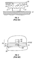
- Fig. 2 is an enlarged end view of the slider 22 and a section of the disk 12 taken in the direction 2-2 in Fig. 1.
- the slider 22 is attached to flexure 23 and has an air-bearing surface (ABS) 27 facing the disk 12 and a trailing surface 25 generally perpendicular to the ABS.
- ABS 27 causes the airflow from the rotating disk 12 to generate a bearing of air that supports the slider 20 in very close proximity to or near contact with the surface of disk 12.
- the read/write head 24 is formed on the trailing surface 25 and is connected to the disk drive read/write electronics by electrical connection to terminal pads 29 on the trailing surface 25.
- Fig. 3 is a view in the direction 3-3 of Fig. 2 and shows the ends of read/write head 24 as viewed from the disk 12.
- the read/write head 24 is a series of thin films deposited and lithographically patterned on the trailing surface 25 of slider 22.
- the write head includes magnetic write poles P1/S2 and P1 separated by a write gap 30.
- the CPP-SV magnetoresistive sensor or read head 100 is located between two magnetic shields S1 and P1/S2, with P1/S2 also serving as the first write pole for the write head.
- the shields S1, S2 are formed of magnetically permeable material and are electrically conductive so they can function as the electrical leads to the read head 100. Separate electrical leads may also be used, in which case the read head 100 is formed in contact with layers of electrically conducting lead material, such as tantalum, gold, or copper, that are in contact with the shields S1, S2.
- Fig. 4 is an enlarged sectional view showing the layers making up sensor 100.
- Sensor 100 is a CPP-SV read head comprising a stack of layers formed between the two magnetic shield layers S1, S2 that are typically electroplated NiFe alloy films.
- the lower shield S1 is typically polished by chemical-mechanical polishing (CMP) to provide a smooth substrate for the growth of the sensor stack.
- CMP chemical-mechanical polishing
- the sensor layers include a reference ferromagnetic layer 120 having a fixed magnetic moment or magnetization direction 121 oriented transversely (into the page), a free ferromagnetic layer 110 having a magnetic moment or magnetization direction 111 that can rotate in the plane of layer 110 in response to transverse external magnetic fields from the disk 12, and an electrically conducting spacer layer 130, typically copper (Cu), between the reference layer 120 and free layer 110.
- a reference ferromagnetic layer 120 having a fixed magnetic moment or magnetization direction 121 oriented transversely (into the page)
- a free ferromagnetic layer 110 having a magnetic moment or magnetization direction 111 that can rotate in the plane of layer 110 in response to transverse external magnetic fields from the disk 12
- an electrically conducting spacer layer 130 typically copper (Cu), between the reference layer 120 and free layer 110.
- the reference layer 120 is part of the well-known antiparallel (AP) pinned structure, also called a "laminated" pinned layer, as described in U.S. Patent 5,465,185.
- the AP-pinned structure minimizes magnetostatic coupling of the reference layer 120 with the free layer 110.
- the AP-pinned structure comprises the reference ferromagnetic (AP2) layer 120 and a lower ferromagnetic (AP1) layer 122 that are antiferromagnetically coupled across an AP coupling (APC) layer 123, such as Ru or Ir.
- the AP1 and AP2 ferromagnetic layers have their respective magnetization directions 127, 121 oriented antiparallel.
- the AP-pinned structure may be "self-pinned” or the AP1 layer 122 may have its magnetization direction pinned by being exchange-coupled to an antiferromagnetic (AF) layer 124 or a hard magnetic layer.
- AF antiferromagnetic
- the bottom electrical lead 126 Located between the lower shield layer S1 and the AP-pinned structure are the bottom electrical lead 126 and a seed layer 125.
- the seed layer 125 may be a single layer or multiple layers of different materials.
- the capping layer 112 may be a single layer or multiple layers of different materials, such as a Cu/Ru/Ta trilayer.
- the magnetization direction 111 of free layer 110 will rotate while the magnetization direction 121 of reference layer 120 will remain fixed and not rotate.
- a sense current Is is applied from top lead 113 perpendicularly through the stack to bottom lead 126, the magnetic fields from the recorded data on the disk will cause rotation of the free-layer magnetization 111 relative to the reference-layer magnetization 121, which is detectable as a change in electrical resistance.
- the leads 126, 113 are typically Ta. However, a lower resistance material may also be used. They are optional and used to adjust the shield-to-shield spacing. If the leads 126 and 113 are not present, the bottom and top shields S1 and S2 are used as leads.
- the seed layer 125 is typically one or more layers of NiFeCr, NiFe, Ta, Cu or Ru.
- the antiferromagnetic layer 124 is typically a Mn alloy, e.g., PtMn, NiMn, FeMn, IrMn, PdMn, PtPdMn or RhMn. If a hard magnetic layer is used instead of an antiferromagnetic layer it is typically a CoPt or FePt alloy, for example CoPtCr.
- the capping layer 112 provides corrosion protection and is typically formed of Ru or Ta.
- the ferromagnetic layers 122 (AP1), 120 (AP2), and 110 (free layer) are typically formed of an alloy of one or more of Co, Fe and Ni, or a bilayer of two alloys, such as a CoFeNiFe bilayer.
- reference ferromagnetic layer 120 may be a CoFe alloy, typically 10 to 30 ⁇ thick
- the free ferromagnetic layer 110 may be a bilayer of a CoFe alloy, typically 10-15 ⁇ thick and formed on the spacer layer 130, with a NiFe alloy, typically 10-30 ⁇ thick, formed on the CoFe layer of the bilayer.
- a hard magnetic layer (not shown), such as a CoPt or CoCrPt layer, may also be included outside the sensor stack near the side edges of the free ferromagnetic layer 110 or in the stack for magnetic stabilization or longitudinal biasing of the free ferromagnetic layer 110.
- the read head 100 shown in FIG. 4 is a "bottom-pinned" read head because the AP-pinned structure is below the free layer 110, the free layer 110 can be located below the AP-pinned structure. In such an arrangement the layers of the AP-pinned structure are reversed, with the AP2 layer 120 on top of and in contact with the spacer layer 130.
- the AP1 and AP2 ferromagnetic layers are typically less than about 30 ⁇ thick and the Ru APC layer is greater than about 7 ⁇ thick, typically between 7-10 ⁇ .
- the films of the AP-pinned structure can be reliably sputter deposited to single Angstrom or less accuracy.
- the films are typically deposited at a rate of near 1 ⁇ /s by opening a shutter and depositing for a given time at a given rate.
- the differences in antiferromagnetic exchange coupling energy in CoFeB/Ru/CoFeB trilayers as the Ru APC thickness is moved from moved from 7 to 12 ⁇ thickness in 1 ⁇ steps have been described by N. Wiese et al., Appl. Phys. Lett ., Vol. 85, No. 11, 13 September 2004
- the present invention is the CPP-SV read head as described above with an improved AP-pinned structure, as illustrated in Fig. 5.
- Each of the ferromagnetic layers AP1 and AP2 has a thickness greater than 30 ⁇ , preferably greater than approximately 50 ⁇ , and the APC layer is either Ru or Ir with a thickness less than 7 ⁇ , preferably about 5 ⁇ or less.
- the ultrathin APC layer especially if formed of iridium (Ir), provides significant coupling strength to allow thick ferromagnetic layers to be used for AP1 and AP2 without reducing Hs.
- the AP1 and AP2 layers are preferably CoFe, with the Fe content being between approximately 5 and 80 atomic percent.
- the AP2 layer may be laminated to further enhance bulk spin-dependent scattering.
- NiFe with around 15-25 atomic percent Fe is a strong bulk scatterer and thus laminations with NiFe are useful to further enhance ⁇ R/R.
- a laminated AP2 layer may be a CoFe/NiFe or CoFe/NiFe/CoFe trilayer.
- Cu is also a useful lamination material because CoFe/Cu and NiFe/Cu interfaces provide high interfacial spin-dependent scattering.
- One or more of the free layer, the AP2 layer, the capping layer and the conductive nonmagnetic spacer layer may also include a nano-oxide layer to locally confine the current path and increase the effective resistivity.
- a CoFe nano-oxide layer may be formed, for example, by interrupting the deposition after some CoFe has been deposited and oxidizing its surface for several minutes in an O 2 or O 2 /Ar gas at 0.1-10 Torr.
- Nano-oxide layers can be formed by oxidizing other materials, e.g., Cu/Al alloys.
- CPP-SV samples were made with a 40 ⁇ CoFe free layer, a 25 ⁇ Cu spacer layer and the AP-pinned structure of this invention.
- the AP-pinned structure was made with a 5 ⁇ Ir APC layer and various AP1 and AP2 layers.
- the CPP stack was defined by electron-beam lithography and had a diameter of about 100 nm. Table 1 below lists the measured CPP-SV sensor ⁇ R/R and the AP-pinned structure Hs for these samples.
- the AP1 and AP2 layers have about same magnetic moment, and thus should have the about same thickness.
- AP1 should be thicker than AP2 to cancel out magnetic stray fields on the free layer.
- the moments of AP1 and AP2 in the samples of Table 1 are matched.
- the AP1 layer is 2 ⁇ thinner than the AP2 layer to account for the "dead" layer at the interface between the AP2 layer and the Cu spacer layer.
Landscapes
- Engineering & Computer Science (AREA)
- Physics & Mathematics (AREA)
- Chemical & Material Sciences (AREA)
- Nanotechnology (AREA)
- Condensed Matter Physics & Semiconductors (AREA)
- General Physics & Mathematics (AREA)
- Crystallography & Structural Chemistry (AREA)
- Manufacturing & Machinery (AREA)
- Hall/Mr Elements (AREA)
- Magnetic Heads (AREA)
Applications Claiming Priority (1)
| Application Number | Priority Date | Filing Date | Title |
|---|---|---|---|
| US10/977,300 US7289304B2 (en) | 2004-10-29 | 2004-10-29 | Current-perpendicular-to-the-plane (CPP) magnetoresistive sensor with improved antiparallel-pinned structure |
Publications (2)
| Publication Number | Publication Date |
|---|---|
| EP1653242A2 true EP1653242A2 (de) | 2006-05-03 |
| EP1653242A3 EP1653242A3 (de) | 2008-09-10 |
Family
ID=35825301
Family Applications (1)
| Application Number | Title | Priority Date | Filing Date |
|---|---|---|---|
| EP05105151A Withdrawn EP1653242A3 (de) | 2004-10-29 | 2005-06-13 | CPP magnetoresistiver Sensor und CPP Lesekopf |
Country Status (3)
| Country | Link |
|---|---|
| US (1) | US7289304B2 (de) |
| EP (1) | EP1653242A3 (de) |
| CN (1) | CN100461264C (de) |
Families Citing this family (5)
| Publication number | Priority date | Publication date | Assignee | Title |
|---|---|---|---|---|
| US7356909B1 (en) * | 2004-09-29 | 2008-04-15 | Headway Technologies, Inc. | Method of forming a CPP magnetic recording head with a self-stabilizing vortex configuration |
| US7602590B2 (en) * | 2005-01-12 | 2009-10-13 | Headway Technologies, Inc. | Tunneling magneto-resistive spin valve sensor with novel composite free layer |
| US7679866B2 (en) * | 2006-09-21 | 2010-03-16 | Hitachi Global Storage Technologies Netherlands B.V. | CPP spin valve with long spin diffusion length AP1 layers |
| US8227023B1 (en) * | 2009-05-27 | 2012-07-24 | Western Digital (Fremont), Llc | Method and system for fabricating magnetic transducers with improved pinning |
| US8873204B1 (en) | 2014-07-25 | 2014-10-28 | HGST Netherlands B.V. | Current-perpendicular-to-the-plane (CPP) magnetoresistive (MR) sensor structure with multiple stacked sensors and center shield with CoFeB insertion layer |
Family Cites Families (19)
| Publication number | Priority date | Publication date | Assignee | Title |
|---|---|---|---|---|
| US5408377A (en) * | 1993-10-15 | 1995-04-18 | International Business Machines Corporation | Magnetoresistive sensor with improved ferromagnetic sensing layer and magnetic recording system using the sensor |
| US5465185A (en) * | 1993-10-15 | 1995-11-07 | International Business Machines Corporation | Magnetoresistive spin valve sensor with improved pinned ferromagnetic layer and magnetic recording system using the sensor |
| US5583725A (en) * | 1994-06-15 | 1996-12-10 | International Business Machines Corporation | Spin valve magnetoresistive sensor with self-pinned laminated layer and magnetic recording system using the sensor |
| SG46731A1 (en) * | 1995-06-30 | 1998-02-20 | Ibm | Spin valve magnetoresistive sensor with antiparallel pinned layer and improved exchange bias layer and magnetic recording system using the senor |
| US5880913A (en) * | 1997-10-27 | 1999-03-09 | International Business Machines Corporation | Antiparallel pinned spin valve sensor with read signal symmetry |
| US5920446A (en) * | 1998-01-06 | 1999-07-06 | International Business Machines Corporation | Ultra high density GMR sensor |
| US6303218B1 (en) * | 1998-03-20 | 2001-10-16 | Kabushiki Kaisha Toshiba | Multi-layered thin-film functional device and magnetoresistance effect element |
| US6209193B1 (en) * | 1998-08-24 | 2001-04-03 | International Business Machines Corporation | Method of making read sensor with self-aligned low resistance leads |
| JP2001143223A (ja) * | 1999-11-11 | 2001-05-25 | Alps Electric Co Ltd | スピンバルブ型薄膜磁気素子及び薄膜磁気ヘッド |
| US6680831B2 (en) * | 2000-09-11 | 2004-01-20 | Matsushita Electric Industrial Co., Ltd. | Magnetoresistive element, method for manufacturing the same, and method for forming a compound magnetic thin film |
| US6704175B2 (en) * | 2001-03-28 | 2004-03-09 | Tdk Corporation | Current perpendicular-to-the-plane magnetoresistance read head |
| US6807033B2 (en) * | 2002-01-23 | 2004-10-19 | Carnegie Mellon University | Magnetic sensor with reduced wing region magnetic sensitivity |
| US6741432B2 (en) * | 2002-03-21 | 2004-05-25 | International Business Machines Corporation | Current perpendicular to the planes (CPP) spin valve sensor with in-stack biased free layer and self-pinned antiparallel (AP) pinned layer structure |
| US6751072B2 (en) | 2002-03-21 | 2004-06-15 | Hitachi Global Storage Technologies Netherlands B.V. | High magnetoresistance spin valve sensor with self-pinned antiparallel (AP) pinned layer structure |
| US6865062B2 (en) * | 2002-03-21 | 2005-03-08 | International Business Machines Corporation | Spin valve sensor with exchange biased free layer and antiparallel (AP) pinned layer pinned without a pinning layer |
| US6903904B2 (en) * | 2002-10-22 | 2005-06-07 | Headway Technologies, Inc. | CPP GMR synthetic spin valve enhancement |
| US6943994B2 (en) * | 2003-02-13 | 2005-09-13 | Headway Technologies, Inc. | Design of canted synthetic pattern exchange spin valve head for improving stability and bias |
| US7265946B2 (en) * | 2003-04-30 | 2007-09-04 | Hitachi Global Storage Technologies Netherlands B.V. | Multilayer self-pinned structure for CPP GMR |
| US6865109B2 (en) * | 2003-06-06 | 2005-03-08 | Seagate Technology Llc | Magnetic random access memory having flux closure for the free layer and spin transfer write mechanism |
-
2004
- 2004-10-29 US US10/977,300 patent/US7289304B2/en not_active Expired - Fee Related
-
2005
- 2005-06-13 EP EP05105151A patent/EP1653242A3/de not_active Withdrawn
- 2005-09-01 CN CNB2005100980212A patent/CN100461264C/zh not_active Expired - Fee Related
Also Published As
| Publication number | Publication date |
|---|---|
| CN1767002A (zh) | 2006-05-03 |
| CN100461264C (zh) | 2009-02-11 |
| US7289304B2 (en) | 2007-10-30 |
| US20060092580A1 (en) | 2006-05-04 |
| EP1653242A3 (de) | 2008-09-10 |
Similar Documents
| Publication | Publication Date | Title |
|---|---|---|
| US8014109B2 (en) | Current-perpendicular-to-the-plane (CPP) magnetoresistive sensor with antiparallel-pinned layer containing silicon | |
| US7826182B2 (en) | Current-perpendicular-to-the-plane (CPP) magnetoresistive sensor with CoFeGe ferromagnetic layers | |
| US8514525B2 (en) | Current-perpendicular-to-the-plane (CPP) magnetoresistive (MR) sensor with reference layer integrated in magnetic shield | |
| US8208228B2 (en) | Current-perpendicular-to-the-plane (CPP) magnetoresistive read head with multiple sensing elements for patterned-media | |
| US8233247B2 (en) | Scissoring-type current-perpendicular-to-the-plane giant magnetoresistance (CPP-GMR) sensors with damped free layer structures | |
| US9047892B2 (en) | Current-perpendicular-to-the-plane (CPP) magnetoresistive (MR) sensor having an antiparallel free (APF) structure with improved magnetic stability | |
| US8611053B2 (en) | Current-perpendicular-to-the-plane (CPP) magnetoresistive sensor with multilayer reference layer including a Heusler alloy | |
| US8351165B2 (en) | Current-perpendicular-to-the-plane (CPP) magnetoresistive sensor with CoFeGe ferromagnetic layers and Ag or AgCu spacer layer | |
| US8218270B1 (en) | Current-perpendicular-to-the-plane (CPP) magnetoresistive (MR) sensor with improved hard magnet biasing structure | |
| US8385025B2 (en) | Current-perpendicular-to-the-plane (CPP) magnetoresistive (MR) sensor with improved seed layer structure for hard bias layer | |
| JP4912207B2 (ja) | 反平行フリー層構造および低電流誘起ノイズの面直電流型(cpp)磁気抵抗センサ | |
| US20120063034A1 (en) | Current-perpendicular-to-the-plane (cpp) magnetoresistive (mr) sensor with improved insulating structure | |
| US9076467B2 (en) | Current-perpendicular-to-the-plane (CPP) magnetoresistive sensor with multilayer reference layer including a crystalline CoFeX layer and a Heusler alloy layer | |
| US7551409B2 (en) | Current-perpendicular-to-the-plane (CPP) magnetoresistive sensor with improved ferromagnetic free layer structure | |
| US7957107B2 (en) | Current-perpendicular-to-the-plane (CPP) magnetoresistive sensor with antiparallel-free layer structure and low current-induced noise | |
| US20130064971A1 (en) | Method for making a current-perpendicular-to-the-plane (cpp) magnetoresistive (mr) sensor with an antiparallel free (apf) structure formed of an alloy requiring post-deposition high temperature annealing | |
| US8576519B1 (en) | Current-perpendicular-to-the-plane (CPP) magnetoresistive (MR) sensor with magnetic damping material at the sensor edges | |
| US8670218B1 (en) | Current-perpendicular-to-the-plane (CPP) magnetoresistive (MR) sensor with hard magnet biasing structure having a MgO insulating layer | |
| US7599157B2 (en) | Current-perpendicular-to-the-plane (CPP) magnetoresistive sensor with high-resistivity amorphous ferromagnetic layers | |
| US20080112095A1 (en) | Dual current-perpendicular-to-the-plane (cpp) magnetoresistive sensor with heusler alloy free layer and minimal current-induced noise | |
| US20030161077A1 (en) | Magnetoresistance effect device and magnetoresistance effect head comprising the same, and magnetic recording/reproducing apparatus | |
| US7423847B2 (en) | Current-perpendicular-to-the-plane spin-valve (CPP-SV) sensor with current-confining apertures concentrated near the sensing edge | |
| US9047891B1 (en) | Current-perpendicular-to-the-plane giant magnetoresistance (CPP-GMR) sensor with indium-zinc-oxide (IZO) spacer layer | |
| US8852963B2 (en) | Method for making a current-perpendicular-to-the-plane (CPP) magnetoresistive sensor having a low-coercivity reference layer | |
| US7289304B2 (en) | Current-perpendicular-to-the-plane (CPP) magnetoresistive sensor with improved antiparallel-pinned structure |
Legal Events
| Date | Code | Title | Description |
|---|---|---|---|
| PUAI | Public reference made under article 153(3) epc to a published international application that has entered the european phase |
Free format text: ORIGINAL CODE: 0009012 |
|
| AK | Designated contracting states |
Kind code of ref document: A2 Designated state(s): AT BE BG CH CY CZ DE DK EE ES FI FR GB GR HU IE IS IT LI LT LU MC NL PL PT RO SE SI SK TR |
|
| AX | Request for extension of the european patent |
Extension state: AL BA HR LV MK YU |
|
| PUAL | Search report despatched |
Free format text: ORIGINAL CODE: 0009013 |
|
| AK | Designated contracting states |
Kind code of ref document: A3 Designated state(s): AT BE BG CH CY CZ DE DK EE ES FI FR GB GR HU IE IS IT LI LT LU MC NL PL PT RO SE SI SK TR |
|
| AX | Request for extension of the european patent |
Extension state: AL BA HR LV MK YU |
|
| 17P | Request for examination filed |
Effective date: 20081127 |
|
| AKX | Designation fees paid |
Designated state(s): DE FR GB |
|
| 17Q | First examination report despatched |
Effective date: 20091007 |
|
| STAA | Information on the status of an ep patent application or granted ep patent |
Free format text: STATUS: THE APPLICATION IS DEEMED TO BE WITHDRAWN |
|
| 18D | Application deemed to be withdrawn |
Effective date: 20100218 |