EP1653280A1 - Systeme et procede d'exposition de motif - Google Patents
Systeme et procede d'exposition de motif Download PDFInfo
- Publication number
- EP1653280A1 EP1653280A1 EP04745543A EP04745543A EP1653280A1 EP 1653280 A1 EP1653280 A1 EP 1653280A1 EP 04745543 A EP04745543 A EP 04745543A EP 04745543 A EP04745543 A EP 04745543A EP 1653280 A1 EP1653280 A1 EP 1653280A1
- Authority
- EP
- European Patent Office
- Prior art keywords
- pattern
- light
- exposure
- optical unit
- optical
- Prior art date
- Legal status (The legal status is an assumption and is not a legal conclusion. Google has not performed a legal analysis and makes no representation as to the accuracy of the status listed.)
- Withdrawn
Links
Images


Classifications
-
- G—PHYSICS
- G03—PHOTOGRAPHY; CINEMATOGRAPHY; ANALOGOUS TECHNIQUES USING WAVES OTHER THAN OPTICAL WAVES; ELECTROGRAPHY; HOLOGRAPHY
- G03F—PHOTOMECHANICAL PRODUCTION OF TEXTURED OR PATTERNED SURFACES, e.g. FOR PRINTING, FOR PROCESSING OF SEMICONDUCTOR DEVICES; MATERIALS THEREFOR; ORIGINALS THEREFOR; APPARATUS SPECIALLY ADAPTED THEREFOR
- G03F7/00—Photomechanical, e.g. photolithographic, production of textured or patterned surfaces, e.g. printing surfaces; Materials therefor, e.g. comprising photoresists; Apparatus specially adapted therefor
- G03F7/70—Microphotolithographic exposure; Apparatus therefor
- G03F7/70691—Handling of masks or workpieces
- G03F7/70791—Large workpieces, e.g. glass substrates for flat panel displays or solar panels
-
- G—PHYSICS
- G03—PHOTOGRAPHY; CINEMATOGRAPHY; ANALOGOUS TECHNIQUES USING WAVES OTHER THAN OPTICAL WAVES; ELECTROGRAPHY; HOLOGRAPHY
- G03F—PHOTOMECHANICAL PRODUCTION OF TEXTURED OR PATTERNED SURFACES, e.g. FOR PRINTING, FOR PROCESSING OF SEMICONDUCTOR DEVICES; MATERIALS THEREFOR; ORIGINALS THEREFOR; APPARATUS SPECIALLY ADAPTED THEREFOR
- G03F7/00—Photomechanical, e.g. photolithographic, production of textured or patterned surfaces, e.g. printing surfaces; Materials therefor, e.g. comprising photoresists; Apparatus specially adapted therefor
- G03F7/70—Microphotolithographic exposure; Apparatus therefor
- G03F7/70008—Production of exposure light, i.e. light sources
- G03F7/7005—Production of exposure light, i.e. light sources by multiple sources, e.g. light-emitting diodes [LED] or light source arrays
-
- G—PHYSICS
- G03—PHOTOGRAPHY; CINEMATOGRAPHY; ANALOGOUS TECHNIQUES USING WAVES OTHER THAN OPTICAL WAVES; ELECTROGRAPHY; HOLOGRAPHY
- G03F—PHOTOMECHANICAL PRODUCTION OF TEXTURED OR PATTERNED SURFACES, e.g. FOR PRINTING, FOR PROCESSING OF SEMICONDUCTOR DEVICES; MATERIALS THEREFOR; ORIGINALS THEREFOR; APPARATUS SPECIALLY ADAPTED THEREFOR
- G03F7/00—Photomechanical, e.g. photolithographic, production of textured or patterned surfaces, e.g. printing surfaces; Materials therefor, e.g. comprising photoresists; Apparatus specially adapted therefor
- G03F7/70—Microphotolithographic exposure; Apparatus therefor
- G03F7/70216—Mask projection systems
- G03F7/70258—Projection system adjustments, e.g. adjustments during exposure or alignment during assembly of projection system
-
- G—PHYSICS
- G03—PHOTOGRAPHY; CINEMATOGRAPHY; ANALOGOUS TECHNIQUES USING WAVES OTHER THAN OPTICAL WAVES; ELECTROGRAPHY; HOLOGRAPHY
- G03F—PHOTOMECHANICAL PRODUCTION OF TEXTURED OR PATTERNED SURFACES, e.g. FOR PRINTING, FOR PROCESSING OF SEMICONDUCTOR DEVICES; MATERIALS THEREFOR; ORIGINALS THEREFOR; APPARATUS SPECIALLY ADAPTED THEREFOR
- G03F7/00—Photomechanical, e.g. photolithographic, production of textured or patterned surfaces, e.g. printing surfaces; Materials therefor, e.g. comprising photoresists; Apparatus specially adapted therefor
- G03F7/70—Microphotolithographic exposure; Apparatus therefor
- G03F7/70216—Mask projection systems
- G03F7/70275—Multiple projection paths, e.g. array of projection systems, microlens projection systems or tandem projection systems
-
- G—PHYSICS
- G03—PHOTOGRAPHY; CINEMATOGRAPHY; ANALOGOUS TECHNIQUES USING WAVES OTHER THAN OPTICAL WAVES; ELECTROGRAPHY; HOLOGRAPHY
- G03F—PHOTOMECHANICAL PRODUCTION OF TEXTURED OR PATTERNED SURFACES, e.g. FOR PRINTING, FOR PROCESSING OF SEMICONDUCTOR DEVICES; MATERIALS THEREFOR; ORIGINALS THEREFOR; APPARATUS SPECIALLY ADAPTED THEREFOR
- G03F7/00—Photomechanical, e.g. photolithographic, production of textured or patterned surfaces, e.g. printing surfaces; Materials therefor, e.g. comprising photoresists; Apparatus specially adapted therefor
- G03F7/70—Microphotolithographic exposure; Apparatus therefor
- G03F7/70383—Direct write, i.e. pattern is written directly without the use of a mask by one or multiple beams
- G03F7/70391—Addressable array sources specially adapted to produce patterns, e.g. addressable LED arrays
-
- G—PHYSICS
- G03—PHOTOGRAPHY; CINEMATOGRAPHY; ANALOGOUS TECHNIQUES USING WAVES OTHER THAN OPTICAL WAVES; ELECTROGRAPHY; HOLOGRAPHY
- G03F—PHOTOMECHANICAL PRODUCTION OF TEXTURED OR PATTERNED SURFACES, e.g. FOR PRINTING, FOR PROCESSING OF SEMICONDUCTOR DEVICES; MATERIALS THEREFOR; ORIGINALS THEREFOR; APPARATUS SPECIALLY ADAPTED THEREFOR
- G03F7/00—Photomechanical, e.g. photolithographic, production of textured or patterned surfaces, e.g. printing surfaces; Materials therefor, e.g. comprising photoresists; Apparatus specially adapted therefor
- G03F7/70—Microphotolithographic exposure; Apparatus therefor
- G03F7/70483—Information management; Active and passive control; Testing; Wafer monitoring, e.g. pattern monitoring
- G03F7/70605—Workpiece metrology
- G03F7/70616—Monitoring the printed patterns
- G03F7/70641—Focus
-
- G—PHYSICS
- G03—PHOTOGRAPHY; CINEMATOGRAPHY; ANALOGOUS TECHNIQUES USING WAVES OTHER THAN OPTICAL WAVES; ELECTROGRAPHY; HOLOGRAPHY
- G03F—PHOTOMECHANICAL PRODUCTION OF TEXTURED OR PATTERNED SURFACES, e.g. FOR PRINTING, FOR PROCESSING OF SEMICONDUCTOR DEVICES; MATERIALS THEREFOR; ORIGINALS THEREFOR; APPARATUS SPECIALLY ADAPTED THEREFOR
- G03F9/00—Registration or positioning of originals, masks, frames, photographic sheets or textured or patterned surfaces, e.g. automatically
- G03F9/70—Registration or positioning of originals, masks, frames, photographic sheets or textured or patterned surfaces, e.g. automatically for microlithography
- G03F9/7003—Alignment type or strategy, e.g. leveling, global alignment
- G03F9/7023—Aligning or positioning in direction perpendicular to substrate surface
- G03F9/7026—Focusing
Definitions
- the present invention relates to a pattern exposing apparatus and a pattern exposing method for performing exposure for a wiring pattern on a substrate.
- an example of a method for forming a micro-sized pattern in order of submicron is a reduction projection exposing method in which a mask pattern is projected on a substrate and exposed in a reduced manner.
- the reduction projection exposing method has a problem in that a desired pattern can not be obtained.
- the exposure is carried out in a short time with respect to a large panel substrate in which an exposure field is set to be broad and which has such a size that one side thereof is more than 1m. Therefore, the defocus caused by a curve of the panel substrate becomes unignorable.
- a pattern exposing apparatus in which a convergent laser beam is irradiated on the panel substrate according to CAD data such as a wiring pattern.
- CAD data such as a wiring pattern.
- a pattern exposing apparatus employing a direct lithography method has been proposed.
- the pattern exposing apparatus employing a direct lithography method is disclosed in Patent Document 1.
- the pattern exposing apparatus disclosed in Patent Document 1 includes (i) a condensing lens for condensing laser light on a photosensitive material applied on a panel substrate, the laser light emitted from a laser light source (ii) a focus error signal detection apparatus for measuring a distance between the condensing lens and the photosensitive material, and (iii) an actuator which moves the condensing lens in an optical axial direction. Then, the pattern exposing apparatus performs focus servo so as to keep a constant distance between the condensing lens and the photosensitive material. The focus servo allows to perform the exposure in which, despite curves on the panel substrate, the laser light passed through the condensing lens focuses on the photosensitive material. This makes it possible to obtain a uniform pattern.
- Patent Document 1 only has one laser source (for example, a semiconductor laser) and one condensing lens, and thus has a problem in that an exposure process for a large panel substrate requires very long time.
- the pattern exposing apparatus disclosed in Patent Document 1 may be so arranged as to include a plurality of optical units each of which has a laser source and a condensing lens. This arrangement allows to expose in a plurality of patterns at the same time.
- characteristics of each optical unit refers to characteristics of each of the laser sources or error in positional adjustment of each optical unit, characteristics of an optical element provided in each optical unit, and the like.
- the pattern exposing apparatus including a plurality of optical units, due to the difference in characteristics of each optical unit (the uneven characteristics of each optical unit), has a problem in that the exposure cannot be performed in accordance with a pattern faithful to pattern data concerning a target exposure pattern.
- the present invention is to solve the above mentioned problems and an object of the present invention is to provide a pattern exposing apparatus and a pattern exposing method, by each of which the pattern exposing apparatus comprising a plurality of optical units can perform the exposure in accordance with patterns faithful to pattern data regardless of the uneven characteristics of each optical unit, the pattern data concerning target exposure patterns.
- a pattern exposing apparatus includes: (I) optical units, each of which has (i) a light source for emitting laser light for exposure in a scanning manner and (ii) a light condensing lens for condensing the laser light onto a photosensitive material applied on a panel substrate; and (II) a control section for transmitting, respectively to each optical unit, a control signal according to pattern data concerning a target exposure pattern, the control signal being for controlling a width of pattern to be formed by exposure, each optical unit respectively exposing the photosensitive material in accordance with a pattern according to the control signal in the scanning manner, the pattern exposing apparatus further including a compensation section for compensating individually the control signals according to characteristics of the corresponding optical units, the control signals being to be transmitted from the control section to the corresponding optical units.
- the pattern exposing apparatus includes the plurality of optical units.
- each optical unit has variation in characteristics of the light source.
- each optical unit has variation in the adjustment errors in positioning an optical element in each optical unit.
- characteristics of the optical element provided in each optical unit are various.
- the characteristics of the light source, the adjustment error in positioning each optical element, and the characteristics of the optical element are dependent on the characteristics of each optical unit.
- the variation (non-uniformity) in characteristics of the respective optical units cause variation in widths of patterns to be formed by exposure performed by the respective optical units.
- the above mentioned arrangement includes a compensation section, which compensates the control signal to be sent from the control section to each optical unit according to the characteristics of each optical unit.
- the width of pattern to be formed by exposure is adjusted according to the control signal which is compensated according to its characteristics.
- each optical unit adjusts, according to the control signal in which the characteristics of each optical unit are compensated, the width of pattern to be formed by exposure.
- a method in accordance with the present invention is a pattern exposing method for exposing a photosensitive material in accordance with a pattern in a scanning manner by using a pattern exposing apparatus including a plurality of optical units having (i) a light source for emitting laser light for the exposure in the scanning manner and (ii) a light condensing lens for condensing the laser light onto the photosensitive material applied on a panel substrate.
- the method includes the steps of: transmitting, respectively to each optical unit, a control signal according to pattern data concerning a target exposure pattern, the control signal being for controlling a width of pattern to be formed by exposure; and compensating individually the control signals according to characteristics of the corresponding optical units, the control signals being to be transmitted from the control section to the corresponding optical units.
- the pattern exposing apparatus includes the plurality of optical units.
- each optical unit has variation in characteristics of the light source.
- each optical unit has variation in the adjustment errors in positioning an optical element in each optical unit.
- characteristics of the optical element provided in each optical unit are various.
- the characteristics of the light source, the adjustment error in positioning each optical element, and the characteristics of the optical element are dependent on the characteristics of each optical unit.
- the variation (non-uniformity) in characteristics of the respective optical units cause variation in widths of patterns to be formed by exposures performed by the respective optical units.
- the above mentioned procedure includes the step of compensating individually the control signals according to characteristics of the corresponding optical units, the control signals being to be transmitted from the control section to the corresponding optical units.
- each optical unit adjusts, according to the control signal which is compensated according to its characteristics respectively, width of pattern to be formed by exposure.
- each optical unit adjusts, according to the control signal in which the characteristics of each optical unit are compensated, the width of pattern to be formed by exposure.
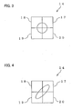
- Fig. 1 schematically illustrates an arrangement of a pattern exposing apparatus 30 according to Embodiment 1.
- the pattern exposing apparatus 30 includes a plurality of optical units 1, an XYZ stage 11, a panel substrate 10, data transfer means 22, control means 23, a plurality of compensation operation memories (compensation means) 24.
- the XYZ stage 11 is a rectangular stage. Directions of sides thereof are an x direction, a y direction and a z direction respectively.
- the XYZ stage 11 is for mounting the panel substrate 10 thereon.
- the X direction is a direction parallel to a width direction of a base of the XYZ stage 11
- the Y direction is a direction parallel to a length direction of the base of the XYZ stage 11
- the Z direction is a direction vertical to the X direction and the Y direction.
- the XYZ stage 11 is movable in the X direction or in the Y direction. This allows the panel substrate 10 to be scanned in the X direction or in the Y direction.
- the XYZ stage 11 on which the panel substrate 10 is mounted is moved. However, it may be arranged such that the XYZ stage 11 is in a fixed position and each optical unit 1 is moved.
- the panel substrate 10 on which a photosensitive material is applied is mounted on the XYZ stage 11 such that a surface thereof on which the photosensitive material is applied faces the optical unit 1.
- the data transfer means (data transfer circuit) 22 is an apparatus for externally receiving data concerning an exposure target pattern (desired pattern) (hereinafter referred to as "pattern data"), and for transferring the pattern data to the control means 23.
- pattern data which is created using a CAD system, indicates a wiring pattern which is to be formed on the panel substrate.
- the pattern data created using the CAD system is transferred by the data transfer means 22 to the control means 23.
- the control means (control circuit) 23 is a circuit for outputting to an optical unit 1 a control signal for controlling a width of pattern to be formed by exposure, the control signal being according to the pattern data transferred from the data transfer means 22.
- the control means 23 respectively generates different control signals for each optical unit 1, and respectively sends the different control signals to each optical unit 1.
- Each compensation operation memory (lookup table, compensation means) 24 is a circuit for compensating the control signals being respectively sent from the control means 23 to the optical units 1 according to the characteristics of the corresponding optical units 1.
- the compensation operation memories 24 respectively correspond to the optical units 1.
- Each compensation operation memory 24 stores therein compensation data according to the characteristics of the optical unit corresponding thereto.
- a plurality of compensation operation memories 24 as compensation means is provided, but it may be arranged such that compensation data which respectively correspond to each optical unit is stored in one compensation means.
- the optical unit 1 is an apparatus for irradiating laser light on the photosensitive material applied on the panel substrate 10.
- the optical unit 1 irradiates the laser light on the photosensitive material in accordance with the control signal sent from the compensation operation memory 24 corresponding to the optical unit 1, so as to form a pattern on the photosensitive material.
- each optical unit 1 is respectively connected to each compensation operation memory 24, and each compensation operation memory 24 is connected to the control means 23.
- the data transfer means 22, the control means 23, a compensation operation memory 24a and an optical unit 1a are cascade-connected in this order
- the data transfer means 22, the control means 23, a compensation operation memory 24b, and an optical unit 1b are cascade-connected in this order.
- the optical unit 1 controls a width of pattern to be formed by exposure.
- the pattern width is adjusted by controlling the optical unit 1 according to the control signal so as to adjust a focus position of an optical system for condensing laser light on the photosensitive material.
- the pattern width is adjusted by controlling the optical unit 1 according to the control signal so as to adjust intensity of the laser light.
- the first method is described in Embodiment 1.
- the second method will be described in Embodiment 2.
- the exposure of the photosensitive material on the panel substrate 10 is performed with the plurality of optical unit 1. Accordingly, a plurality of light condensing points is formed on a surface of the photosensitive material. Moreover, the exposure is performed on the panel substrate 10 being scanned in the X direction or in the Y direction. Therefore, one scan performed can cause the plurality of optical units 1 to expose to form a plurality of patterns on the photosensitive material on the panel substrate 10.
- the control means 23 outputs the control signals that are to be inputted into the corresponding optical units 1.
- the output of each control signal is carried out according to the pattern data transferred from the data transfer means 22, and each control signal is respectively compensated by the corresponding compensation operation memory 24.
- each optical unit 1 performs the exposure of the photosensitive material on the panel substrate 10 in a scanning manner.
- each compensation operation memory 24 compensates the inputted control signal according to the characteristics of the corresponding optical unit. Therefore, the optical units 1 can perform the exposure of the photosensitive material respectively to form patterns faithful to the pattern data regardless of the characteristics thereof. Detailed descriptions for the optical unit 1 and the compensation operation memory 24 will be given below.
- the optical unit 1 includes a semiconductor laser (light source) 2, a collimator lens 3, a beam splitter (hereinafter referred to as "BS") 4, a first light-receiving element 5, a polarization beam splitter (hereinafter referred to as PBS) 6, a 1/4-wavelength plate 7, a first light condensing lens 8, an actuator 9, an error signal detection apparatus 15, and focus servo control means 16.
- BS beam splitter
- PBS polarization beam splitter
- the optical unit 1 is arranged such that light emitted from the semiconductor laser 2 passes through the collimator lens 3, the BS 4, the PBS 6, the 1/4-wavelength plate 7, and the first light condensing lens 8 in this order, and the light is condensed on the photosensitive material on the panel substrate 10.
- the light condensed on the photosensitive material on the panel substrate 10 is reflected therefrom.
- the reflected light passes through the first light condensing lens 8, the 1/4-wavelength plate 7 and the PBS 6 in this order, and then enters the error signal detecting apparatus 15.
- the semiconductor laser 2 is a laser light source for emitting laser light to which the photosensitive material is sensitive.
- the collimator lens 3 is for shaping laser light emitted from the semiconductor laser 2 (for example, for shaping the laser light into light of parallel beams), and for guiding the shaped laser light into the BS 4.
- the BS 4 is an optical element which reflects a part of the laser light from the collimator lens 3 to the first light-receiving element 5 and which lets the rest of the laser light pass therethrough and guides it to the PBS 6.
- the first light-receiving element 5 receives the laser light from the BS 4 thereby to monitor intensity of the laser light outputted from the semiconductor laser 2.
- the PBS 6 is an optical element which guides the laser light from the BS 4 to the 1/4-wavelength plate 7 by reflecting the laser light. Meanwhile, the PBS 6 lets the reflected light pass therethrough, the reflected light reflected from the photosensitive material on the panel substrate 10. By doing this, the PBS 6 guides the reflected light to the error signal detection apparatus 15.
- the 1/4-wavelength plate 7 is an optical element, by which light entered therein is so outputted that the outputted light has a 1/4-wavelength shift between phases of a polarization component which is in parallel direction to a crystal axis of the 1/4-wavelength plate and of a polarization component which is vertical to the crystal axis.
- the laser light from the PBS 6 is converted from linear polarization light to circular polarization light by the 1/4-wavelength plate 7.
- the reflected light from the photosensitive material is converted from circular polarization light to linear polarization light by the 1/4-wavelength plate 7.
- the 1/4-wavelength plate 7 shifts a polarization plane, whereby the output light passed through the 1/4-wavelength plate 7 is shifted by 90° in comparison with the incident light on the 1/4-wavelength plate 7.
- the first light condensing lens 8 condenses light from the 1/4-wavelength plate 7 on the photosensitive material on the panel substrate 10.
- the error signal detection apparatus (focus error detection means) 15 is a unit for outputting a focus error signal (hereinafter referred to as FES) indicating a focus error of the first light condensing lens 8 according to the light reflected on the photosensitive material on the panel substrate 10 and passed through the first light condensing lens 8, the 1/4-wavelength plate 7, and the PBS 6.
- FES focus error signal
- the focus serve-control means 16 drives the actuator 9 according to the FES to perform focus servo.
- the compensation operation memory 24 is connected to the focus servo-control means 16, which is provided in the optical unit 1 corresponding to the compensation operation memory 24.
- the focus servo-control means 16 adjusts the offset voltage according to the control signal, and adds the adjusted offset voltage to the FES thereby to perform the focus servo.
- the actuator 9 moves the first light condensing lens 8 in the optical axial direction, and adjusts a distance between the photosensitive material and the first light condensing lens 8.
- an FES detection method examples include an astigmatic method, a knife-edge method, etc.
- an arrangement in which the astigmatic method is used to detect the FES will be described. It should be noted that an arrangement in which the knife-edge method is used to detect the FES is also possible.
- the error signal detection apparatus 15 includes a second light condensing lens 12, a cylindrical lens 13, and a second light-receiving element 14. Specifically, on the light axis of the light reflected on the photosensitive material on the panel substrate 10, the first light condensing lens 8, the 1/4-wavelength plate 7, the PBS 6, the second light condensing lens 12, the cylindrical lens 13, and the second light-receiving element 14 are arranged in this order.
- the second light condensing lens 12 condenses, on the second light-receiving element 14, the light which is reflected from the photosensitive material and passed through the first light condensing lens 8, the 1/4-wavelength plate 7, and the PBS 6.
- the cylindrical lens 13 condenses one direction of light from the second light condensing lens 12, in order to astigmatize the light.
- the second light-receiving element 14 is a so-called tetrametric light-receiving element whose light-receiving surface is divided into four.
- the second light-receiving element 14 receives the light passed through the second light condensing lens 12 and the cylindrical lens 13 (the reflected light from the photosensitive material on the panel substrate 10) on each light-receiving surface, and converts, into an electronic signal, the light received on each light-receiving surface.
- first light-receiving surface 17 a first light-receiving surface 17, a second light-receiving surface 18, a third light-receiving surface 19, and a fourth light-receiving element 20 respectively.
- the first light-receiving surface 17 and the third light-receiving surface 19 are in a diagonal relationship
- the second light-receiving surface 18 and the fourth light-receiving surface 20 are in a diagonal relationship.
- a positional relationship among the second light condensing lens 12, the cylindrical lens 13, and the second light-receiving element 14 is set such that a circular pattern form of light is obtained on the second light-receiving element 14 when the focal point of the first light condensing lens 8 is on the photosensitive material applied on the panel substrate 10.
- the four light-receiving surfaces receive the same amount of light, so that the outputs of the four light-receiving surfaces are equal. Therefore, the FES is 0.
- the positional relationship among the second light condensing lens 12, the cylindrical lens 13, and the second light-receiving element 14 is set such that when the distance between the first light condensing lens 8 and the photosensitive material is more than the focal distance of the first light condensing lens 8, an oval pattern form is obtained on the second light-receiving element 14, as illustrated in Fig. 4, and the amount of light received on the first light-receiving surface 17 and the third light-receiving surface 19 is more than the amount of light received on the second light-receiving surface 18 and the fourth light-receiving surface 20.
- the error detection apparatus 15 may be arranged such that the FES is negative when the distance between the first light condensing lens 8 and the photosensitive material is more than the focal distance of the first light condensing lens 8, and the FES is positive when the distance between the first light condensing lens 8 and the photosensitive material is less than the focal distance of the first condensing lens 8.
- the pattern exposing apparatus 30 of Embodiment 1 is arranged such that it includes a plurality of optical units 1. If the pattern exposing apparatus 30 was not include each compensation operation memory 24, the form of laser light outputted from each optical unit 1 would not be uniform, even if currents applied to the semiconductor laser 2 are the same and the focus servo is adjusted for allowing the FES to be 0 in all the optical units 1, resulting in variation in the widths of patterns to be formed by exposure by the optical unit 1. That is, even if each optical unit has the same target width of pattern to be formed by exposure, the widths of pattern to be formed by exposure by the respective optical units in reality are not uniform.
- each optical unit 1 has variation in positional adjustment errors in fixing optical element therein. Furthermore, characteristics of the optical element provided in each optical unit are not uniform.
- the characteristics of the semiconductor laser 2, the positional adjustment errors in fixing each optical element, and the characteristics of the optical element are referred to the "characteristics of each optical unit”.
- Variation in widths of patterns to be formed by exposure by each optical unit 1 is referred to "exposure non-uniformity”. The variation in pattern widths is caused by variations in the characteristics of each optical unit.
- each optical unit 1 can not expose to form, on the panel substrate 10, a pattern faithful to the pattern data.
- Embodiment 1 is provided with the compensation operation memory 24, which compensates, according to the characteristics of each optical unit 1, the control signal sent from the control means 23 to each optical unit 1. That is, each compensation operation memory 24 stores compensation data according to the characteristics of each optical unit 1 connected to each compensation operation memory 24. The control signal is compensated according to the compensation data. When each optical unit 1 is set up, the compensation data is set according to the characteristics of each optical unit 1 so as to eliminate the exposure non-uniformity.
- each optical unit 1 is allowed to actually perform exposure to form a pattern according to pattern data which is identical with each other in terms of the targeted exposure pattern width of each optical unit 1. Then, a control signal to be inputted to each optical unit 1 is multiplied by a coefficient in each case in order that each optical unit 1 actually performs the exposures in a uniform pattern. Coefficients thus calculated are stored as a compensation data in each compensation operation memory 24 corresponding to each optical unit 1.
- each optical unit 1 can expose to form, on the panel substrate 10, a pattern faithful to the pattern data regardless of the characteristics of each optical unit.
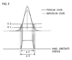
- the laser light indicated by a solid line in Fig. 5 has a focus position on a surface of the photosensitive material
- the laser light indicated by a broken line in Fig. 5 has a focus position which is distanced from the surface of the photosensitive material by a distance d. That is, the laser light indicated by the solid line is in a focusing state, and the laser light indicated by the broken line is in a defocus state with a defocus amount d.
- the photosensitive material is a negative resist and the photosensitive material has a characteristic that a photo-reaction is initiated with the light exposure amount of E1, and is completed with the light exposure amount of E2.
- Fig. 5 indicates a developed pattern form. From Fig. 5, it can be seen that the pattern width x2 formed by the laser light in the defocusing state is wider than the pattern width x1 formed by the laser light in the focusing state.
- the exposure pattern widths x1 and x2 illustrated in Fig. 5 are measured on the surface of the panel substrate 10.
- the focus position of the first light condensing lens 8 arranged in any optical unit 1 is adjusted by the amount of defocus d, it is possible to form uniform widths of patterns by each of the optical units 1.
- the amount of defocus d is illustrated larger than the actual amount of defocus for the sake of easy explanation in the description of Embodiment 1. However, the amount of defocus d is actually very small.
- the following description explains a method for adjusting the focus position of the first light condensing lens 8 by the amount of defocus d in the optical unit 1.
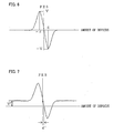
- Fig. 6 is a graph of a characteristic curve illustrating a relationship between a voltage of the FES detected by the error signal detection apparatus 15 and an amount of defocus of the first light condensing lens 8.
- the horizontal axis indicates the amount of defocus
- a vertical axis indicates the voltage of the FES.
- the focus servo control means 16 performs the focus servo by driving the actuator 9 such that the voltage of the FES becomes 0. As a result, the amount of defocus becomes 0.
- Fig. 7 illustrates a graph of a characteristic curve illustrating a relationship between a voltage of the FES and an amount of defocus.
- an offset voltage V' is added to this voltage of the FES.
- the horizontal axis indicates the amount of defocus
- the vertical axis indicates the voltage of the FES.
- the focus servo control means 16 performs the focus servo by driving the actuator 9 such that the voltage of the FES becomes 0. As a result, the defocus amount becomes d'.
- the range of the amount of defocus of -d to d can be a target of the focus servo if a voltage in the range from -V to +V is added as an offset voltage V' to the FES in Fig. 6 (the voltage in the range from -V to +V correspond to an amount of defocus in the range from -d to d).
- This allows the distance between the first light condensing lens 8 and the photosensitive material on the panel substrate 10 to be adjusted, in the range of the amount of defocus of -d to d, for each optical unit 1.
- Embodiment 1 it is arranged such that the compensation operation memory 24 is connected with the focus servo control means 16, and a control signal sent from the compensation operation memory 24 is inputted to the focus servo control means 16.
- the focus servo control means 16 adjusts, according to the control signal, the offset voltage V' that is to be added to the FES. Then, the offset current which is adjusted according to the control signal is added to the FES so as to perform the focus servo. In this way, the width of pattern to be formed by exposure performed by the corresponding optical unit 1 is adjusted according to pattern data.
- the control signal is compensated by the compensation operation memory 24. Therefore, a pattern faithful to the pattern data can be formed on the panel substrate 10 by the exposure regardless of the characteristics of each optical unit 1. That is, when each optical unit 1 aims to form the pattern with the same pattern width, each optical unit 1 can perform exposure to actually form the pattern with a uniform pattern width. Therefore, the pattern exposing apparatus 30 according to Embodiment 1 does not cause exposure non-uniformity when plural patterns are formed by laser light from a plural number of optical units 1. Accordingly, it is possible to form a pattern faithful to the pattern data.
- the focus servo control means 16 adjusts the offset voltage V' according to the control signal which is compensated by the compensation operation memory 24. Then, the focus servo control means 16 adds the adjusted offset voltage V' to the FES and performs the focus servo to set the FES to 0. However, the focus servo can be performed by setting the target voltage according to the control signal which is compensated by the compensation operation memory 24 in order to adjust the FES to the target voltage.
- the focus servo control means 16 may have any arrangement, provided that the focus servo control means 16 allows to adjust the focus position of the first light condensing lens 8 in the optical axial direction, according to (a) the FES detected by the error signal detection apparatus 15 and on (b) the control signal.
- the method has been explained in which the focus servo allows each optical unit 1 to form a pattern faithful to the pattern data, regardless of the exposure incoherence of each optical unit 1.
- the method may include the following problems.
- a metal film or the like is partially formed on the panel substrate 10 to form for example a thin film transistor or the like. Therefore, in practice, various types or forms of the metal film cause changes in an amount of light which is reflected from the panel substrate 10, and thus in an amount of light received in a second light-receiving element 14.
- the changes in an amount of light received in the second light-receiving element 14 cause changes in a signal amplitude of the FES as illustrated in Fig. 8. Due to the changes in a signal amplitude of the FES, as illustrated in Fig. 8, the target position of the focus servo changes from the amount of defocus d1 to the amount of defocus d2.
- the focus servo control means 16 compensates the focus position of the first light condensing lens 8 according to the amount of all light received by the second light-receiving element 14. Specifically, it may be arranged such that the amount of all light received by the second light-receiving element 14 is multiplied by a predetermined coefficient so as to obtain an offset voltage V'. Alternatively, it may be arranged such that an offset voltage V' is added to a value obtained by dividing the FES by the amount of all light received. In either of these ways, it is possible to appropriately maintain the focus position of the first light condensing lens 8 and the position of the photosensitive material, even if the amount of reflected light changes.
- Embodiment 1 it is arranged such that the intensity of the semiconductor laser 2 in each optical unit 1 is fixed, and the position of the first light condensing lens 8 in each optical unit 1 is adjusted in the optical axial direction, so as to control each width of pattern to be formed by exposure.
- intensity of the semiconductor laser in each optical unit is variable, and the intensity of the semiconductor laser is adjusted in each optical unit, so as to control each width of pattern to be formed by exposure.
- Embodiment 2 only arrangement different from Embodiment 1 is explained.
- Fig. 13 illustrates an arrangement of an optical unit 101 according to Embodiment 2.
- the optical unit 101 illustrated in Fig. 13 is different from the optical unit 1 illustrated in Fig. 2 in that the optical unit 101 includes a laser driver (intensity changing means) 25 which is connected with a compensation operation memory 24 and a semiconductor laser 2.
- This laser driver 25 adjusts the current to be applied to the semiconductor laser 2 in accordance with the control signal sent from the compensation operation memory 24, so as to adjust the intensity of the laser light of the semiconductor laser 2.
- the photosensitive material is a negative resist and has a characteristic that photo-reaction is initiated with the light exposure amount E1 and that the photo-reaction is completed with the light exposure amount E2.
- a pattern width formed by the laser light with the intensity of I2 is x3 and a pattern width formed by the laser light with the intensity of I3 is x4.
- the pattern width formed by the laser light with the intensity of I2 is narrower than the pattern width formed by the laser light with the intensity of I3. That is, different intensities of the laser light lead to different widths of patterns to be formed by exposure.
- each optical unit 101 a current to be applied to the semiconductor laser 2 is adjusted by the laser driver 25 in accordance with the control signal from the compensation operation memory 24. This makes it possible not only to form a pattern on the panel substrate 10 according to the pattern data, but also to adjust the width of pattern to be formed by exposure performed by each optical unit 101.
- each optical unit 101 can perform the exposure to form a pattern faithful to the pattern data on the panel substrate 10 regardless of the characteristics of each optical unit 101. That is, when the target pattern widths targeted by each optical unit 101 are the same, each optical unit 101 can actually perform the exposure to form uniform pattern width.
- the intensity of the semiconductor laser 2 can be more easily adjusted in an arrangement in which a first light-receiving element (monitor means) 5 monitors the laser light outputted from the semiconductor laser 2 and the laser driver 25 compensates the intensity of the laser light of the semiconductor laser 2 in accordance with the monitoring result from the first light-receiving element 5.
- a first light-receiving element (monitor means) 5 monitors the laser light outputted from the semiconductor laser 2 and the laser driver 25 compensates the intensity of the laser light of the semiconductor laser 2 in accordance with the monitoring result from the first light-receiving element 5.
- Embodiment 1 and Embodiment 2 can be used.
- a method combining Embodiment 1 and Embodiment 2 may also be used.
- Embodiment 3 For actually forming a pattern on a photosensitive material, it is necessary to perform the exposure such that a pattern is drawn(formed) in a variety of forms. For this purpose, a method for exposing a pattern in an arbitrary form will be described in Embodiment 3. In Embodiment 3, only arrangement different from Embodiment 1 and Embodiment 2 is explained.
- the optical unit 1 exposes the photosensitive material to laser light with the intensity of I4.
- the intensity I4 is, as illustrated in Fig. 11, an intensity that gives an exposure amount E1 or less to the photosensitive material (the exposure amount E1 is an amount enough to cause the photosensitive material to be photo-reacted). That is, the intensity I4 is an intensity that is less than an intensity that causes the photosensitive material to be photo-reacted, i.e. an intensity that does not cause the photosensitive material to be photo-reacted.
- the intensity I1 is an intensity that gives the photosensitive material an exposure amount enough to cause the photosensitive material to be photo-reacted (that is, an intensity that causes the photosensitive material to be photo-reacted).
- the offset voltage to the FES remains 0. Then, when the laser light arrives at the position y2, the offset voltage V' is added to the FES, so as to perform the exposure to form a pattern with focus servo that targets the amount of defocus amount d'. Further, when the condensed light beam is arrived at the position y3, the intensity of the laser light is set to I4.
- the offset voltage is accordingly changed according to the targeted pattern form. This makes it possible to obtain exposure patterns in various forms.
- the intensity of the laser light outputted by the semiconductor laser 2 is accordingly changed. This makes it possible to obtain exposure patterns in various forms.
- an area which is not to be exposed (for example an area up to the position y1 which is a starting point of the exposure) is previously irradiated with laser light with the intensity of I1, which is less than the light exposure amount E1, and it is preferable to previously perform the focus servo.
- the optical unit 1 it is preferable to arrange the optical unit 1 such that the width of pattern to be formed by exposure by the optical unit 1 in the focus state (focusing state) is narrower than the target minimum exposure pattern width. In other words, it is preferable that optical units 1 can form a pattern as small as possible. The reason for this will be explained below.
- the width of the pattern to be formed on the photosensitive material by the exposure can be easily widened by defocusing the optical unit 1.
- narrowing the pattern width can be realized by adjusting the amount of defocus of the optical unit 1 close to 0. That is, a width of pattern to be formed by exposure by the optical unit 1 in the focusing state (defocus amount is 0) is the minimum width which can be formed by the exposure.
- the width of pattern to be formed by exposure in the focusing state is widened. This may lead to a disadvantage in that the exposure in the targeted minimum pattern cannot be attained.
- the intensity of the laser light outputted by the semiconductor laser 2 is lowered in order to narrow the pattern width of the pattern to be formed on the photosensitive material, an angle of a pattern wall becomes more gentle, as shown in Fig. 12, but no practical form of a pattern can be realized. Moreover, in this case, the formed pattern width is not so narrow.
- the optical unit 1 it is preferable to arrange the optical unit 1 such that even if the variation in semiconductor lasers 2 or the positional error in the optical elements degrades light condensing performance, the light condensing performance is enough to perform the exposure to form the targeted minimum pattern, that is, the width of pattern to be formed by exposure by the optical unit 1 in the focus state (focusing state) is narrower than the target minimum exposure pattern width.
- a pattern exposing apparatus includes: (I) optical units, each of which has (i) a light source for emitting laser light for exposure in a scanning manner and (ii) a light condensing lens for condensing the laser light onto a photosensitive material applied on a panel substrate; and (II) a control section for transmitting, respectively to each optical unit, a control signal according to pattern data concerning a target exposure pattern, the control signal being for controlling a width of pattern to be formed by exposure, each optical unit respectively exposing the photosensitive material in accordance with a pattern according to the control signal in the scanning manner, the pattern exposing apparatus further comprising: a compensation section for compensating individually the control signals according to characteristics of the corresponding optical units, the control signals being to be transmitted from the control section to the corresponding optical units.
- the pattern exposing apparatus comprises the plurality of optical units.
- each optical unit has variation in characteristics of the light source.
- each optical unit has variation in the adjustment errors in positioning an optical element in each optical unit.
- characteristics of the optical element provided in each optical unit are various.
- the characteristics of the light source, the adjustment error in positioning each optical element, and the characteristics of the optical element are dependent on the characteristics of each optical unit.
- the variation (non-uniformity) in characteristics of the respective optical units cause variation in widths of patterns to be formed by exposures performed by the respective optical units.
- the above mentioned arrangement comprises compensation means for compensating, according to the characteristics of the corresponding optical unit, the control signal to be sent to the corresponding optical unit from the control means.
- the width of pattern to be formed by exposure is adjusted according to the control signal which is compensated according to its characteristics.
- each optical unit adjusts, according to the control signal in which the characteristics of each optical unit are compensated, the width of pattern to be formed by exposure .
- each optical unit comprises a focus servo control section for adjusting a focus position of the light condensing lens in an optical axial direction according to the control signal.
- the focus servo control means adjusts the focus position of the light condensing lens according to the control signal sent to the optical unit in the optical axial direction, it is possible to control, according to the control signal, the width of pattern to be formed by exposure.
- each optical unit comprises: an intensity changing section for adjusting, according to the control signal, intensity of the laser light to be emitted from the light source.
- the laser light which has intensity above a certain degree causes photoreaction of the photosensitive material. Moreover, a change in the intensity of the laser light emitted from the laser light source cause a change in a width of an area in which the photoreaction of the photosensitive material occurs, and thus the width of pattern to be formed by exposure also changes. Therefore, By adjusting the intensity of the laser light emitted from the light source according to the control signal, it becomes possible to control, according to the control signal, the width of pattern to be formed by exposure.
- a method in accordance with the present invention is a pattern exposing method for exposing a photosensitive material in accordance with a pattern in a scanning manner by using a pattern exposing apparatus comprising a plurality of optical units having (i) a light source for emitting laser light for the exposure in the scanning manner and (ii) a light condensing lens for condensing the laser light onto the photosensitive material applied on a panel substrate.
- the method comprises the steps of: transmitting, respectively to each optical unit, a control signal according to pattern data concerning a target pattern, the control signal being for controlling a width of pattern to be formed by exposure; and compensating individually the control signals according to characteristics of the corresponding optical units, the control signals being to be transmitted from the control section to the corresponding optical units.
- the pattern exposing apparatus comprises the plurality of optical units.
- each optical unit has variation in characteristics of the light source.
- each optical unit has variation in the adjustment errors in positioning an optical element therein.
- characteristics of the optical element provided in each optical unit are various.
- the characteristics of the light source, the adjustment error in positioning the optical element in each optical unit, and the characteristics of the optical element are dependent on the characteristics of each optical unit.
- the variation (non-uniformity) in characteristics of the respective optical units causes variation in widths of patterns to be formed by exposures performed by the respective optical units.
- the above mentioned procedure comprises the step of compensating the control signal sent from the control means to each optical unit according to the characteristics of the corresponding optical unit.
- each optical unit adjusts, according to the control signal which is compensated according to characteristics of the corresponding optical unit, width of pattern to be formed by exposure.
- each optical unit adjusts, according to the control signal in which the characteristics of the corresponding optical unit are compensated, the width of pattern to be formed by exposure.
- exposure in a pattern faithful to the pattern data can be performed on the panel substrate, regardless of the characteristics of each optical unit.
- the pattern exposing method in accordance with the present invention is arranged such that a focus position of the light condensing lens is individually adjusted according to the control signal corresponding thereto in an optical axial direction, so as to control a width of pattern to be formed by exposure performed by the optical unit corresponding thereto.
- the focus position of the light condensing lens to the position on the photosensitive material is moved in the optical axial direction, the beam width on the photosensitive material changes, and thus the width of pattern to be formed by exposure also changes. Therefore, by adjusting the focus position of the light condensing lens according to the control signal sent to the optical unit in optical axial direction, it is possible to control, according to the control signal, the width of pattern to be formed by exposure.
- the pattern exposing method in accordance with the present invention is arranged such that intensity of the laser light emitted from the light source is individually adjusted according to the control signal corresponding thereto, so as to control a width of pattern to be formed by exposure performed by the optical unit corresponding thereto.
- the laser light which has intensity equal to or higher than a certain intensity causes the photoreaction of the photosensitive material. Moreover, a change in the intensity of the laser light emitted from the light source causes a change in a width of an area in which the photoreaction of the photosensitive material occurs, and thus the width of pattern to be formed by exposure also changes. Therefore, by adjusting the intensity of the laser light emitted from the laser light source according to the control signal, it is possible to control, according to the control signal, the width of pattern to be exposed.
- the pattern exposing method in accordance with the present invention is so arranged as to include the steps of: when an optical axis of the light condensing lens intersects with an exposure position on the photosensitive material, adjusting the intensity of the laser light to intensity enough to cause the photosensitive material to be photo-reacted; and when the optical axis of the light condensing lens intersects with a non-exposure position on the photosensitive material, adjusting the intensity of the laser light to intensity less than the intensity enough to cause the photosensitive material to be photo-reacted.
- the intensity of the laser light is adjusted to the intensity enough to cause the photosensitive material to be photo-reacted. This makes it possible to perform pattern exposure on the exposure position.
- the intensity of the laser light is adjusted to the intensity less than the intensity enough to cause the photosensitive material to be photo-reacted. With this step, it is possible to maintain a state in which a pattern is not exposed, while the laser light is emitted in the non-exposure position.
- the pattern exposing method in accordance with the present invention arranged such that a width of pattern to be formed by exposure performed by the optical unit which is equal to or narrower than a target minimum exposure pattern width when the light condensing lens is in a focusing state.
- Widening the exposure pattern width of the exposure of the photosensitive material can be realized by moving the focal position of the light condensing lens away from the photosensitive material.
- narrowing the exposure pattern width can be realized by moving the focus point of the light condensing lens toward the photosensitive material. That is, when the light condensing lens is in the focus state (focusing state), the width of pattern to be formed by exposure by the optical unit has a minimum width.
- the exposure would not be possibly carried out in the target minimum pattern width in case where degradation of the light condensing performance occurs due to the variation in the characteristics of the optical unit.
- the width of pattern to be formed by exposure by the optical unit is equal to or narrower than the target minimum exposure pattern width (i.e. the minimum exposure width has an allowance)
- the width of pattern to be formed by exposure by the optical unit is equal to or narrower than the target minimum exposure pattern width (i.e. the minimum exposure width has an allowance)
- the embodiments above discusses the cases in which data transferring means 22, control means 23, and a compensation operation memory 24 as compensation means are hardware.
- the present invention is not limited to these arrangements. All or a part of each member can be realized by combination of a program for realizing the function and hardware (computer) for executing the program.
- the data transferring means 22, the control means 23, and the compensation means can be realized by using a computer as a device driver for driving the pattern exposing apparatus 30, the computer connected to a pattern exposing apparatus 30.
- the present invention is especially appropriate in the steps of performing pattern exposure for wiring or the like on a large area panel substrate in fabrication of flat type display apparatus such as a liquid crystal panel.
- the present invention is not limited to liquid crystal panel substrate, but is suitably used in steps for exposing for a wiring pattern on the substrate for a variety of electronic circuits.
Landscapes
- Physics & Mathematics (AREA)
- General Physics & Mathematics (AREA)
- Life Sciences & Earth Sciences (AREA)
- Sustainable Development (AREA)
- Exposure And Positioning Against Photoresist Photosensitive Materials (AREA)
- Exposure Of Semiconductors, Excluding Electron Or Ion Beam Exposure (AREA)
Applications Claiming Priority (2)
| Application Number | Priority Date | Filing Date | Title |
|---|---|---|---|
| JP2003206288A JP4312535B2 (ja) | 2003-08-06 | 2003-08-06 | パターン露光装置 |
| PCT/JP2004/007687 WO2005015317A1 (fr) | 2003-08-06 | 2004-06-03 | Systeme et procede d'exposition de motif |
Publications (2)
| Publication Number | Publication Date |
|---|---|
| EP1653280A1 true EP1653280A1 (fr) | 2006-05-03 |
| EP1653280A4 EP1653280A4 (fr) | 2008-06-18 |
Family
ID=34131380
Family Applications (1)
| Application Number | Title | Priority Date | Filing Date |
|---|---|---|---|
| EP04745543A Withdrawn EP1653280A4 (fr) | 2003-08-06 | 2004-06-03 | Systeme et procede d'exposition de motif |
Country Status (3)
| Country | Link |
|---|---|
| EP (1) | EP1653280A4 (fr) |
| JP (1) | JP4312535B2 (fr) |
| WO (1) | WO2005015317A1 (fr) |
Cited By (6)
| Publication number | Priority date | Publication date | Assignee | Title |
|---|---|---|---|---|
| WO2011104178A1 (fr) * | 2010-02-23 | 2011-09-01 | Asml Netherlands B.V. | Appareil lithographique et procédé de fabrication de dispositif |
| WO2014033118A1 (fr) * | 2012-08-27 | 2014-03-06 | Micronic Mydata AB | Écriture sans masque dans différents plans focaux |
| WO2018015113A1 (fr) * | 2016-07-19 | 2018-01-25 | Asml Netherlands B.V. | Procédé de lithographie sans masque à écriture directe |
| US10149390B2 (en) | 2012-08-27 | 2018-12-04 | Mycronic AB | Maskless writing of a workpiece using a plurality of exposures having different focal planes using multiple DMDs |
| WO2020096731A1 (fr) * | 2018-11-08 | 2020-05-14 | Applied Materials, Inc. | Reconnaissance de signal pendant la formation de motifs de substrat par photolithographie numérique |
| US10921717B2 (en) | 2017-10-24 | 2021-02-16 | Canon Kabushiki Kaisha | Exposure apparatus and article manufacturing method |
Families Citing this family (10)
| Publication number | Priority date | Publication date | Assignee | Title |
|---|---|---|---|---|
| JP2006337696A (ja) * | 2005-06-01 | 2006-12-14 | Fujifilm Holdings Corp | 液晶パネルの製造方法 |
| JP2007101592A (ja) * | 2005-09-30 | 2007-04-19 | Nikon Corp | 走査型露光装置及びマイクロデバイスの製造方法 |
| JP4938784B2 (ja) | 2005-10-26 | 2012-05-23 | マイクロニック レーザー システムズ アクチボラゲット | 書込み装置および方法 |
| US8122846B2 (en) | 2005-10-26 | 2012-02-28 | Micronic Mydata AB | Platforms, apparatuses, systems and methods for processing and analyzing substrates |
| CN102770810B (zh) * | 2010-02-23 | 2016-01-06 | Asml荷兰有限公司 | 光刻设备和器件制造方法 |
| WO2014140047A2 (fr) | 2013-03-12 | 2014-09-18 | Micronic Mydata AB | Procédé et dispositif d'écriture de masques photographiques avec réduction des erreurs mura |
| KR102253995B1 (ko) | 2013-03-12 | 2021-05-18 | 마이크로닉 아베 | 기계적으로 생성된 정렬 표식 방법 및 정렬 시스템 |
| JP6694717B2 (ja) * | 2016-01-25 | 2020-05-20 | デクセリアルズ株式会社 | 露光装置および露光方法 |
| WO2019082726A1 (fr) * | 2017-10-24 | 2019-05-02 | キヤノン株式会社 | Dispositif d'exposition et procédé de fabrication d'article |
| JP2019079029A (ja) * | 2017-10-24 | 2019-05-23 | キヤノン株式会社 | 露光装置および物品の製造方法 |
Family Cites Families (17)
| Publication number | Priority date | Publication date | Assignee | Title |
|---|---|---|---|---|
| JPS59146068A (ja) * | 1983-02-08 | 1984-08-21 | Nippon Telegr & Teleph Corp <Ntt> | 記録方法 |
| JPS61277259A (ja) * | 1985-05-31 | 1986-12-08 | Toshiba Corp | レ−ザプリンタ |
| JPS6249315A (ja) * | 1985-08-29 | 1987-03-04 | Konishiroku Photo Ind Co Ltd | レ−ザ記録装置 |
| JPH028809A (ja) * | 1988-06-28 | 1990-01-12 | Asahi Optical Co Ltd | 走査式光学装置及びその調整方法 |
| JP3069587B2 (ja) * | 1988-11-01 | 2000-07-24 | セイコーエプソン株式会社 | 多出力電流供給用集積回路及びそれを用いた複数の被駆動素子の駆動制御装置 |
| JPH02188276A (ja) * | 1989-01-17 | 1990-07-24 | Canon Inc | 画像形成装置 |
| JP2706983B2 (ja) * | 1989-05-19 | 1998-01-28 | キヤノン株式会社 | 焦点調節機構を備えた走査光学装置 |
| JP2680160B2 (ja) * | 1990-02-16 | 1997-11-19 | 日本製紙株式会社 | レーザープロッタ |
| JPH05290720A (ja) * | 1992-04-08 | 1993-11-05 | Sony Corp | 電界放出型マイクロカソードの作製方法 |
| JP3052587B2 (ja) * | 1992-07-28 | 2000-06-12 | 日本電気株式会社 | 露光装置 |
| JP3550037B2 (ja) * | 1999-01-21 | 2004-08-04 | シャープ株式会社 | 露光装置および液晶ディスプレイの製造方法 |
| JP4198835B2 (ja) * | 1999-08-27 | 2008-12-17 | 株式会社沖データ | 書き込み装置、画像形成装置及びledヘッド |
| JP2001125285A (ja) * | 1999-10-29 | 2001-05-11 | Toshiba Corp | パターン描画装置 |
| JP4526732B2 (ja) * | 2001-05-17 | 2010-08-18 | 富士フイルム株式会社 | 光記録システム |
| JP2002131675A (ja) * | 2000-10-26 | 2002-05-09 | Fuji Photo Film Co Ltd | 露光記録装置 |
| JP3583750B2 (ja) * | 2001-11-08 | 2004-11-04 | 大日本スクリーン製造株式会社 | 画像記録装置および出力光量補正方法 |
| US6794626B2 (en) * | 2002-01-15 | 2004-09-21 | Agfa Corporation | Method and system for verifying correct mounting of a printing plate on an external drum imaging machine |
-
2003
- 2003-08-06 JP JP2003206288A patent/JP4312535B2/ja not_active Expired - Fee Related
-
2004
- 2004-06-03 EP EP04745543A patent/EP1653280A4/fr not_active Withdrawn
- 2004-06-03 WO PCT/JP2004/007687 patent/WO2005015317A1/fr not_active Ceased
Cited By (15)
| Publication number | Priority date | Publication date | Assignee | Title |
|---|---|---|---|---|
| CN102763041B (zh) * | 2010-02-23 | 2014-10-22 | Asml荷兰有限公司 | 光刻设备和器件制造方法 |
| CN102763041A (zh) * | 2010-02-23 | 2012-10-31 | Asml荷兰有限公司 | 光刻设备和器件制造方法 |
| WO2011104178A1 (fr) * | 2010-02-23 | 2011-09-01 | Asml Netherlands B.V. | Appareil lithographique et procédé de fabrication de dispositif |
| US10149390B2 (en) | 2012-08-27 | 2018-12-04 | Mycronic AB | Maskless writing of a workpiece using a plurality of exposures having different focal planes using multiple DMDs |
| WO2014033118A1 (fr) * | 2012-08-27 | 2014-03-06 | Micronic Mydata AB | Écriture sans masque dans différents plans focaux |
| US11284517B2 (en) | 2012-08-27 | 2022-03-22 | Micronic Mydata AB | System for direct writing on an uneven surface of a workpiece that is covered with a radiation sensitive layer using exposures having different focal planes |
| WO2018015113A1 (fr) * | 2016-07-19 | 2018-01-25 | Asml Netherlands B.V. | Procédé de lithographie sans masque à écriture directe |
| TWI640839B (zh) * | 2016-07-19 | 2018-11-11 | 荷蘭商Asml荷蘭公司 | 用於直寫無光罩微影之設備 |
| CN109478024A (zh) * | 2016-07-19 | 2019-03-15 | Asml荷兰有限公司 | 用于直接写入无掩模光刻的设备 |
| US10527950B2 (en) | 2016-07-19 | 2020-01-07 | Asml Netherlands B.V. | Apparatus for direct write maskless lithography |
| CN109478024B (zh) * | 2016-07-19 | 2021-03-26 | Asml荷兰有限公司 | 用于直接写入无掩模光刻的设备 |
| US10921717B2 (en) | 2017-10-24 | 2021-02-16 | Canon Kabushiki Kaisha | Exposure apparatus and article manufacturing method |
| WO2020096731A1 (fr) * | 2018-11-08 | 2020-05-14 | Applied Materials, Inc. | Reconnaissance de signal pendant la formation de motifs de substrat par photolithographie numérique |
| US10890852B2 (en) | 2018-11-08 | 2021-01-12 | Applied Materials, Inc. | Signal recognition during substrate patterning via digital photolithography |
| US11397384B2 (en) | 2018-11-08 | 2022-07-26 | Applied Materials, Inc. | Signal recognition during substrate patterning via digital photolithography |
Also Published As
| Publication number | Publication date |
|---|---|
| JP2005055524A (ja) | 2005-03-03 |
| WO2005015317A1 (fr) | 2005-02-17 |
| EP1653280A4 (fr) | 2008-06-18 |
| JP4312535B2 (ja) | 2009-08-12 |
Similar Documents
| Publication | Publication Date | Title |
|---|---|---|
| EP1653280A1 (fr) | Systeme et procede d'exposition de motif | |
| KR100562804B1 (ko) | 공간 광 변조기 배열을 사용하는 마스크리스 리소그래피시스템 및 방법 | |
| US6262792B1 (en) | Optical exposure apparatus of scanning exposure system and its exposing method | |
| US5659383A (en) | Exposure apparatus and exposure quantity control method | |
| JP3308063B2 (ja) | 投影露光方法及び装置 | |
| JP4486323B2 (ja) | 画素位置特定方法、画像ずれ補正方法、および画像形成装置 | |
| US7102733B2 (en) | System and method to compensate for static and dynamic misalignments and deformations in a maskless lithography tool | |
| US8804098B2 (en) | Maskless exposure apparatus having measurement optical unit to measure depths of focus of a plurality of beams and control method thereof | |
| KR20040111029A (ko) | 화소위치 특정방법, 화상어긋남 보정방법 및 화상형성장치 | |
| CN101194209A (zh) | 曝光装置 | |
| KR20090028410A (ko) | 노광 시스템 및 반도체 장치의 제조 방법 | |
| US6400456B1 (en) | Plane positioning apparatus | |
| CN112384861A (zh) | 用于在基板上的无掩模光刻术的实时自动聚焦 | |
| US5793052A (en) | Dual stage following method and apparatus | |
| JP5336036B2 (ja) | 描画システム | |
| JP2006163419A (ja) | 電気光学変調器を使用するシステムおよび方法 | |
| JP3305448B2 (ja) | 面位置設定装置、露光装置、及び露光方法 | |
| KR20100042864A (ko) | 노광장치 및 그 진직도 측정방법 | |
| JP2025038155A (ja) | 露光装置、露光方法およびフラットパネルディスプレイの製造方法、ならびに露光データ作成方法 | |
| JP5209946B2 (ja) | 焦点位置検出方法および描画装置 | |
| US12504691B2 (en) | Drawing apparatus, drawing system, and drawing method | |
| JP4405241B2 (ja) | 液晶ディスプレイ用ガラス基板の露光方法および露光装置ならびに処理装置 | |
| JP4081606B2 (ja) | パターン描画装置およびパターン描画方法 | |
| JP2009086015A (ja) | マスクレス露光装置 | |
| US6956692B2 (en) | Method and apparatus for controlling exposure of a surface of a substrate |
Legal Events
| Date | Code | Title | Description |
|---|---|---|---|
| PUAI | Public reference made under article 153(3) epc to a published international application that has entered the european phase |
Free format text: ORIGINAL CODE: 0009012 |
|
| 17P | Request for examination filed |
Effective date: 20051109 |
|
| AK | Designated contracting states |
Kind code of ref document: A1 Designated state(s): DE SE |
|
| DAX | Request for extension of the european patent (deleted) | ||
| RBV | Designated contracting states (corrected) |
Designated state(s): DE SE |
|
| A4 | Supplementary search report drawn up and despatched |
Effective date: 20080520 |
|
| RIC1 | Information provided on ipc code assigned before grant |
Ipc: G03F 7/00 20060101AFI20050302BHEP Ipc: G06K 15/00 20060101ALI20080514BHEP |
|
| 17Q | First examination report despatched |
Effective date: 20080922 |
|
| STAA | Information on the status of an ep patent application or granted ep patent |
Free format text: STATUS: THE APPLICATION IS DEEMED TO BE WITHDRAWN |
|
| 18D | Application deemed to be withdrawn |
Effective date: 20090403 |