EP1653516A2 - Magnetoresistiver Speicher mit wahlfreiem Zugriff - Google Patents
Magnetoresistiver Speicher mit wahlfreiem Zugriff Download PDFInfo
- Publication number
- EP1653516A2 EP1653516A2 EP05023489A EP05023489A EP1653516A2 EP 1653516 A2 EP1653516 A2 EP 1653516A2 EP 05023489 A EP05023489 A EP 05023489A EP 05023489 A EP05023489 A EP 05023489A EP 1653516 A2 EP1653516 A2 EP 1653516A2
- Authority
- EP
- European Patent Office
- Prior art keywords
- resistance
- variable elements
- lines
- magnetic ram
- current supplying
- Prior art date
- Legal status (The legal status is an assumption and is not a legal conclusion. Google has not performed a legal analysis and makes no representation as to the accuracy of the status listed.)
- Withdrawn
Links
Images



Classifications
-
- H—ELECTRICITY
- H10—SEMICONDUCTOR DEVICES; ELECTRIC SOLID-STATE DEVICES NOT OTHERWISE PROVIDED FOR
- H10D—INORGANIC ELECTRIC SEMICONDUCTOR DEVICES
- H10D84/00—Integrated devices formed in or on semiconductor substrates that comprise only semiconducting layers, e.g. on Si wafers or on GaAs-on-Si wafers
- H10D84/80—Integrated devices formed in or on semiconductor substrates that comprise only semiconducting layers, e.g. on Si wafers or on GaAs-on-Si wafers characterised by the integration of at least one component covered by groups H10D12/00 or H10D30/00, e.g. integration of IGFETs
-
- B—PERFORMING OPERATIONS; TRANSPORTING
- B82—NANOTECHNOLOGY
- B82Y—SPECIFIC USES OR APPLICATIONS OF NANOSTRUCTURES; MEASUREMENT OR ANALYSIS OF NANOSTRUCTURES; MANUFACTURE OR TREATMENT OF NANOSTRUCTURES
- B82Y10/00—Nanotechnology for information processing, storage or transmission, e.g. quantum computing or single electron logic
-
- G—PHYSICS
- G11—INFORMATION STORAGE
- G11C—STATIC STORES
- G11C11/00—Digital stores characterised by the use of particular electric or magnetic storage elements; Storage elements therefor
- G11C11/02—Digital stores characterised by the use of particular electric or magnetic storage elements; Storage elements therefor using magnetic elements
- G11C11/14—Digital stores characterised by the use of particular electric or magnetic storage elements; Storage elements therefor using magnetic elements using thin-film elements
- G11C11/15—Digital stores characterised by the use of particular electric or magnetic storage elements; Storage elements therefor using magnetic elements using thin-film elements using multiple magnetic layers
-
- G—PHYSICS
- G11—INFORMATION STORAGE
- G11C—STATIC STORES
- G11C11/00—Digital stores characterised by the use of particular electric or magnetic storage elements; Storage elements therefor
- G11C11/02—Digital stores characterised by the use of particular electric or magnetic storage elements; Storage elements therefor using magnetic elements
- G11C11/16—Digital stores characterised by the use of particular electric or magnetic storage elements; Storage elements therefor using magnetic elements using elements in which the storage effect is based on magnetic spin effect
-
- G—PHYSICS
- G11—INFORMATION STORAGE
- G11C—STATIC STORES
- G11C11/00—Digital stores characterised by the use of particular electric or magnetic storage elements; Storage elements therefor
- G11C11/02—Digital stores characterised by the use of particular electric or magnetic storage elements; Storage elements therefor using magnetic elements
- G11C11/16—Digital stores characterised by the use of particular electric or magnetic storage elements; Storage elements therefor using magnetic elements using elements in which the storage effect is based on magnetic spin effect
- G11C11/165—Auxiliary circuits
- G11C11/1653—Address circuits or decoders
-
- G—PHYSICS
- G11—INFORMATION STORAGE
- G11C—STATIC STORES
- G11C11/00—Digital stores characterised by the use of particular electric or magnetic storage elements; Storage elements therefor
- G11C11/02—Digital stores characterised by the use of particular electric or magnetic storage elements; Storage elements therefor using magnetic elements
- G11C11/16—Digital stores characterised by the use of particular electric or magnetic storage elements; Storage elements therefor using magnetic elements using elements in which the storage effect is based on magnetic spin effect
- G11C11/165—Auxiliary circuits
- G11C11/1659—Cell access
-
- G—PHYSICS
- G11—INFORMATION STORAGE
- G11C—STATIC STORES
- G11C11/00—Digital stores characterised by the use of particular electric or magnetic storage elements; Storage elements therefor
- G11C11/02—Digital stores characterised by the use of particular electric or magnetic storage elements; Storage elements therefor using magnetic elements
- G11C11/16—Digital stores characterised by the use of particular electric or magnetic storage elements; Storage elements therefor using magnetic elements using elements in which the storage effect is based on magnetic spin effect
- G11C11/165—Auxiliary circuits
- G11C11/1673—Reading or sensing circuits or methods
-
- G—PHYSICS
- G11—INFORMATION STORAGE
- G11C—STATIC STORES
- G11C11/00—Digital stores characterised by the use of particular electric or magnetic storage elements; Storage elements therefor
- G11C11/02—Digital stores characterised by the use of particular electric or magnetic storage elements; Storage elements therefor using magnetic elements
- G11C11/16—Digital stores characterised by the use of particular electric or magnetic storage elements; Storage elements therefor using magnetic elements using elements in which the storage effect is based on magnetic spin effect
- G11C11/165—Auxiliary circuits
- G11C11/1675—Writing or programming circuits or methods
-
- G—PHYSICS
- G11—INFORMATION STORAGE
- G11C—STATIC STORES
- G11C11/00—Digital stores characterised by the use of particular electric or magnetic storage elements; Storage elements therefor
- G11C11/02—Digital stores characterised by the use of particular electric or magnetic storage elements; Storage elements therefor using magnetic elements
- G11C11/16—Digital stores characterised by the use of particular electric or magnetic storage elements; Storage elements therefor using magnetic elements using elements in which the storage effect is based on magnetic spin effect
- G11C11/165—Auxiliary circuits
- G11C11/1693—Timing circuits or methods
-
- G—PHYSICS
- G11—INFORMATION STORAGE
- G11C—STATIC STORES
- G11C11/00—Digital stores characterised by the use of particular electric or magnetic storage elements; Storage elements therefor
- G11C11/56—Digital stores characterised by the use of particular electric or magnetic storage elements; Storage elements therefor using storage elements with more than two stable states represented by steps, e.g. of voltage, current, phase, frequency
- G11C11/5607—Digital stores characterised by the use of particular electric or magnetic storage elements; Storage elements therefor using storage elements with more than two stable states represented by steps, e.g. of voltage, current, phase, frequency using magnetic storage elements
-
- H—ELECTRICITY
- H10—SEMICONDUCTOR DEVICES; ELECTRIC SOLID-STATE DEVICES NOT OTHERWISE PROVIDED FOR
- H10B—ELECTRONIC MEMORY DEVICES
- H10B61/00—Magnetic memory devices, e.g. magnetoresistive RAM [MRAM] devices
- H10B61/20—Magnetic memory devices, e.g. magnetoresistive RAM [MRAM] devices comprising components having three or more electrodes, e.g. transistors
- H10B61/22—Magnetic memory devices, e.g. magnetoresistive RAM [MRAM] devices comprising components having three or more electrodes, e.g. transistors of the field-effect transistor [FET] type
-
- G—PHYSICS
- G11—INFORMATION STORAGE
- G11C—STATIC STORES
- G11C2211/00—Indexing scheme relating to digital stores characterized by the use of particular electric or magnetic storage elements; Storage elements therefor
- G11C2211/56—Indexing scheme relating to G11C11/56 and sub-groups for features not covered by these groups
- G11C2211/561—Multilevel memory cell aspects
- G11C2211/5615—Multilevel magnetic memory cell using non-magnetic non-conducting interlayer, e.g. MTJ
-
- H—ELECTRICITY
- H03—ELECTRONIC CIRCUITRY
- H03L—AUTOMATIC CONTROL, STARTING, SYNCHRONISATION OR STABILISATION OF GENERATORS OF ELECTRONIC OSCILLATIONS OR PULSES
- H03L7/00—Automatic control of frequency or phase; Synchronisation
- H03L7/06—Automatic control of frequency or phase; Synchronisation using a reference signal applied to a frequency- or phase-locked loop
- H03L7/08—Details of the phase-locked loop
- H03L7/085—Details of the phase-locked loop concerning mainly the frequency- or phase-detection arrangement including the filtering or amplification of its output signal
- H03L7/089—Details of the phase-locked loop concerning mainly the frequency- or phase-detection arrangement including the filtering or amplification of its output signal the phase or frequency detector generating up-down pulses
- H03L7/0891—Details of the phase-locked loop concerning mainly the frequency- or phase-detection arrangement including the filtering or amplification of its output signal the phase or frequency detector generating up-down pulses the up-down pulses controlling source and sink current generators, e.g. a charge pump
Definitions
- the invention relates to a magnetic, i.e.magneto-resistive Random Access Memory (RAM).
- RAM Magnetic Random Access Memory
- a magnetic RAM device implements a plurality of resistance-variable components connected to a transistor.
- Such a magnetic RAM is a memory device, which writes information by changing the directions of magnetization of the respective ferromagnetic thin films and reads information by sensing a change in current caused by the change in the directions of the respective ferromagnetic thin films.
- Magnetic RAM is a non-volatile and can achieve high-speed operation, low power consumption, and high-integrity due to the intrinsic characteristics of the ferromagnetic thin films.
- a memory device is implemented using a giant magneto-resistive (GMR) effect or a tunneling magneto-resistive (TMR) effect.
- GMR giant magneto-resistive
- TMR tunneling magneto-resistive
- a magnetic RAM using the GMR effect uses the fact that resistance varies according to whether two magnetic layers having a nonmagnetic layer there between are magnetized in the same direction or in opposite directions.
- a magnetic RAM using a spin polarization magnetic permeability effect uses the fact that the permeability of electrons through an insulation layer interposed between two magnetic layers is greater when the magnetic layers are magnetized in the same direction than in opposite directions.
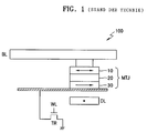
- FIG. 1 shows the structure of a general magnetic RAM.
- FIG. 1 shows a magnetic RAM 100 using the spin polarization magnetic permeability effect.
- the magnetic RAM 100 includes an access transistor TR controlled by a control signal from a word line WL, and a magnetic tunnel junction (MTJ) for storing data that is electrically connected to the access transistor TR.
- the magnetic RAM 100 further includes a digit line DL, and a bit line BL connected to the MTJ.
- the MTJ includes a pinned ferromagnetic layer 30, a tunnel barrier layer 20, and a free ferromagnetic layer 10.
- the magnetization direction of the free ferromagnetic layer 10 can be changed by a current flowing perpendicular to the longitudinal axis of the MTJ. Accordingly, since the digit line DL is aligned perpendicular to the longitudinal axis of the MTJ, a current flowing through the digit line DL can control the magnetization direction of the free ferromagnetic layer 10. In addition, if the bit line BL is aligned perpendicular to the longitudinal axis of the MTJ, a current flowing through the bit line BL can control the magnetization direction of the free ferromagnetic layer 10.
- the bit line BL is to both read and write data, while the digit line DL is used to write data.
- the digit line DL is aligned parallel to the word line WL.
- a sensing current flows through the tunnel barrier layer 20 in a direction perpendicular to the longitudinal axis of the MTJ.
- a magnetization direction of the pinned ferromagnetic layer 30 and the free ferromagnetic layer 10 may be the same direction or an opposite direction according to a magnetization direction of the free ferromagnetic layer 10.
- the magnetization directions of the free ferromagnetic layer 10 and the pinned ferromagnetic layer 30 affect the sensing current.
- the resistance of the MTJ increases, which reduces the sensing current. If the magnetization direction of the free ferromagnetic layer 10 is the same as that of the pinned ferromagnetic layer 30, the resistance of the MTJ decreases, which increases the sensing current.
- Data stored in the magnetic RAM 100 is determined by the resistance.
- the access transistor TR is turned off in response to a signal transferred through the word line WL, thus inducing a current through the digit line DL. If a current flows through the bit line BL, a magnetization direction of the free ferromagnetic layer 10 of the MTJ is determined by a vector sum of the magnetic fields formed by the currents through the digit line DL and the bit line BL.
- the access transistor TR is turned on in response to a signal transferred through the word line WL, thus forming a current path to ground. If the magnetization direction of the free ferromagnetic layer 10 is equal to that of the pinned ferromagnetic layer 30, and accordingly the MTJ has relatively small resistance, a constant current supplied to the bit line BL produces a correspondingly low voltage across the MTJ.
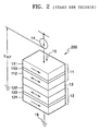
- FIG. 2 shows the structure of a conventional multi-bit magnetic RAM disclosed in Patent Publication US 5,930,164.
- the magnetic RAM 200 has a stacked structure including two MTJs 11 and 12 electrically connected to each other through a conductive layer 13.
- the two MTJs 11 and 12 have different resistances and hysteresis characteristics.
- the two MTJs 11 and 12 can have different resistances. Also, by differentiating the thickness of a free ferromagnetic layer 112 of the MTJ 11 from that of a free ferromagnetic layer 122 of the MTJ 12, the two MTJs 11 and 12 can be switched by different magnetic fields. When data is read, the fact that the resistances of the two MTJ 11 and 12 are different from each other is used.
- the minimum resistance and a maximum resistance of the MTJ 11 are min(R1) and max(R1+ ⁇ R1), respectively, and that the minimum resistance and the maximum resistance of the MTJ 12 are min(R2) and max(R2+ ⁇ R2), respectively.
- the total resistance of the MTJs 11 and 12 is R1+R2.
- the total resistance of the MTJs 11 and 12 is R1+R2+ ⁇ R1.
- the total resistance value of the MTJs 11 and 12 is R1+R2+ ⁇ R2.
- the total resistance of the MTJs 11 and 12 is R1+R2+ ⁇ R1+ ⁇ R2.
- the fact that the hysteresis characteristics of the two MTJs 11 and 12 are different from each other is used. Since the MTJs 11 and 12 are switched by different magnetic fields, due to their different hysteresis characteristics, by adjusting the current flowing through a digit line (not shown), it is possible to write desired multi-bit data in a cell.
- both the direction and magnitude of the magnetic field needs to be adjusted. Also, to write data "01" or "10" a multi-step write process is needed.
- the invention solves this problem by providing a magnetic RAM having the features of claim 1 or 12.
- Advantageous embodiments of the invention are given in the subclaims, the wording of which is herewith incorporated into the specification by reference to avoid unnecessary text repetition.
- a magnetic RAM includes an access transistor formed on a substrate, first through third resistance-variable elements, and first through third current supplying lines.
- the first through third resistance-variable elements are stacked between the access transistor and a bit line, and the first through third resistance-variable elements are electrically connected to each other.
- the first through third resistance-variable elements may have equal resistance characteristics.
- Each of the first through third resistance-variable elements may include a pinned ferromagnetic layer. Magnetization directions of the pinned ferromagnetic layers of two of the first through third resistance-variable elements sharing one of the first through third current supplying lines, through which a bi-directional current flow, may be opposite to each other.
- the same data is written to the two resistance-variable elements sharing one of the first through third current supplying lines, through which a bi-directional current flow.
- a predetermined conductive layer may pass through the first through third current supplying lines.
- the bit line and the second current supplying line may be orthogonal to the first and third current supplying lines.
- the longitudinal axes of the first through third resistance-variable elements may be aligned in parallel with the bit line and the second current supplying line, and data are written to the first through third resistance-variable elements in response to bi-directional currents flowing through the first through third current supplying lines.
- the longitudinal axes of the first through third resistance-variable elements may be perpendicular to the bit line and the second current supplying line, and data are written to the first through third resistance-variable elements in response to bi-directional currents flowing through the bit line and the second current supplying line.
- the first and third resistance-variable elements are made of magneto-resistive material.
- a magnetic RAM includes an access transistor formed on a substrate, first and second resistance-variable elements, and current supplying lines.
- the first and second resistance-variable elements are formed on the access transistor, and the first and second resistance-variable elements are electrically connected to each other.
- a bit line is formed on the second resistance-variable element.
- the current supplying lines are respectively disposed between neighboring two of the access transistor and the first and second resistance-variable elements.
- the first resistance-variable element has different resistance characteristics from the second resistance-variable element.
- a magnetic RAM capable of simultaneously writing or reading n-bit data includes an access transistor formed on a substrate, first through (2 n -1)-th resistance-variable elements, and first through (2 n -1)-th current supplying lines.
- the first through (2 n -1)-th resistance-variable elements are stacked between the access transistor and a bit line, and the first through (2 n -1)-th resistance-variable elements are electrically connected to each other.
- the first through (2 n -1)-th current supplying lines are stacked alternately with the first through (2 n -1)-th resistance-variable elements.
- a magnetic RAM capable of simultaneously writing or reading multi-bit data includes an access transistor formed on a substrate, bit lines and digit lines alternately applied on the access transistor, and a plurality of resistance-variable elements disposed between the bit lines and the digit lines, electrically connected to each other.
- FIG. 3A shows a magnetic RAM 300 according to an embodiment of the invention.
- first through third current supplying lines CSL1, CSL2, and CSL3 are disposed, respectively, between a first resistance-variable element MTJ1 and a second resistance-variable element MTJ2, between the second resistance-variable element MTJ2 and a third resistance-variable element MTJ3, and between the third resistance-variable element MTJ3 and an access transistor TR.
- the first through third resistance-variable elements MTJ1, MTJ2, and MTJ3 are disposed between the access transistor TR and a bit line BL.
- the first through third resistance-variable elements MTJ1, MTJ2, and MTJ3 are electrically connected to each other by a conductive layer EC2.
- the bit line BL is connected to the first resistance-variable layer MTJ1 by a conductive layer EC1.
- the conductive layer EC2 is connected to the access transistor TR via a conductive layer EC3.
- the first through third resistance-variable elements MTJ1, MTJ2, and MTJ3 are composed of a magneto-resistive material.
- the magneto-resistive material may be one of a MTJ (Magnetic Tunnel Junction) material, a GMR (Giant Magneto-Resistive) material, a spin valve, a ferromagnetic/metal/semiconductor hybrid structure, a III-V magnetic semiconductor composite structure, a metal/semiconductor composite structure, or a CMR.
- the second current supplying line CSL2 is aligned parallel to the bit line BL.
- the first current supplying line CSL1 and the third current supplying line CSL3, which are parallel, are orthogonal to the bit line BL.
- a voltage applied to the bit line BL is measured or currents flowing through the first through third resistance-variable elements MTJ1, MTJ2, and MTJ3 are measured. Since data are written to the respective first through third resistance-variable elements MTJ1, MTJ2, and MTJ3 using the first through third current supplying lines CSL1, CSL2, and CSL3, it is possible to easily write multi-bit data. That is, current adjustment for controlling a magnetic field is not needed during a data write operation, and multiple write operations for writing data "01" and "10" are not needed.
- the second resistance-variable element MTJ2 is connected to the third resistance-variable element MTJ3 by the second conductive layer EC2 passing through the second current supplying line CSL2.
- FIG. 3B shows the structure of the second current supplying line CSL2.
- the magnetization directions of the pinned ferromagnetic layers of the first and second resistance-variable elements MTJ1 and MTJ2 are opposite to each other if a current flowing through the first current supplying line CSL1 is a bi-directional current.
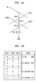
- FIG. 4A is an equivalent circuit diagram of the magnetic RAM 300 of FIG. 3A.
- FIG. 4B is a table for explaining the states of data written to the magnetic RAM of FIG. 3A.
- the first through third resistance-variable elements MTJ1, MTJ2, and MTJ3 have equal resistance characteristics.
- Each of the first through third resistance-variable elements MTJ1, MTJ2, and MTJ3 has a minimum resistance value of R and a maximum resistance of R+ ⁇ R.
- each of the first through third resistance-variable elements MTJ1, MTJ2, and MTJ3 has a resistance of R
- each of the first through third resistance-variable elements MTJ1, MTJ2, and MTJ3 has a resistance of R+ ⁇ R.
- the magnetic RAM 300 can store data "11". That is, the magnetic RAM 300 can store 2-bit data using the first through third resistance-variable elements MTJ1, MTJ2, and MTJ3 with the same resistance characteristics.
- the magnetic RAM 300 can have two structures according to the type of a current supplying line through which the bi-directional current flows.
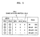
- FIG. 5 is a table for explaining data written to the magnetic RAM 300 of FIG. 3A.
- the longitudinal axes of the first through third resistance-variable elements MTJ1, MTJ2, and MTJ3 are aligned in parallel to the bit line BL and the second current supplying line CSL2.
- data are written to the first through third resistance-variable elements MTJ1, MTJ2, and MTJ3 in response to bi-directional currents flowing through the first and third current supplying lines CSL1 and CSL3.
- Currents flowing through the bit line BL and the second current supplying line CSL2 are one-directional currents and currents flowing through the first and third current supplying lines CSL1 and CSL3 are bi-directional currents.
- the same data can be written to the first and second resistance-variable elements MTJ1 and MTJ2 by the current flowing through the first current supplying line CSL1.
- the same data is written to two of the first through third resistance-variable elements MTJ1, MTJ2, and MTJ3, sharing one of the first or third current supplying lines CSL1 and CSL3 transmitting a bi-directional current.
- the first resistance-variable element MTJ1 stores data in response to a current flowing the bit line BL in a predetermined direction and a current flowing through the first current supplying line CSL1 in one of two directions.
- the second resistance-variable element MTJ2 stores data in response to a current through the second current supplying line CSL2 in a predetermined direction and a current flowing through the first current supplying line CSL1 in one of two directions.
- the third resistance-variable element MTJ3 stores data in response to a current flowing through the second current supplying line CSL2 in a predetermined direction and a current flowing through the third current supplying line CSL3 in one of two directions.
- the first and second resistance-variable elements MTJ1 and MTJ2 receive and store the same data from the first current supplying line CSL1
- the third resistance-variable element MTJ3 receives and stores data from the third current supplying line CSL3.
- the resistance value of the third resistance-variable elements MTJ3 increases, thereby writing data "1" in the third resistance-variable element MTJ3.
- the first through third resistance-variable elements MTJ1, MTJ2, and MTJ3 can store four states of data, that is, 2-bit data.
- a predetermined current is applied to the first through third resistance-variable elements MTJ1, MTJ2, and MTJ3, thus generating a constant voltage across the bit line BL according to the total resistance of the first through third resistance-variable elements MTJ1, MTJ2, and MTJ3. Then, by measuring the generated voltage, 2-bit data written to the first through third resistance-variable elements MTJ1, MTJ2, and MTJ3 can be read.
- FIG. 6A shows a magnetic RAM 600 in which the longitudinal directions of the first through third resistance-variable elements MTJ1, MTJ2, and MTJ3 are different from those of the magnetic RAM 300 shown in FIG. 3A.
- FIG. 6B is a table for explaining data written to the magnetic RAM 600 shown FIG. 6A.
- the longitudinal directions of first through third resistance-variable elements MTJ1, MTJ2, and MTJ3 are aligned perpendicular to a bit line BL and a second current supplying line CSL2.
- data is written by a current flowing in a direction perpendicular to the longitudinal directions of the first through third resistance-variable elements MTJ1, MTJ2, and MTJ3. That is, referring to FIG. 6A, data are written to the first through third resistance-variable elements MTJ 1, MTJ2, and MTJ3 in response to bi-directional currents flowing through the bit line BL and the second current supplying line CSL2.
- data are written to the first through third resistance-variable elements MTJ1, MTJ2, and MTJ3 according to the directions of currents flowing through the bit line BL and the second current supplying line CSL2. For example, if a current flows in the left direction through the bit line BL, since the direction of the generated magnetic field is opposite to the magnetization direction of the pinned ferromagnetic layer of the first resistance-variable element MTJ1, the resistance of the first resistance-variable element MTJ1 increases, thereby writing "1" in the first resistance-variable element MTJ1.
- the resistance of the first resistance-variable element MTJ1 decreases, thereby writing "0" in the first resistance-variable element MTJ1.
- the first through third resistance-variable elements MTJ1, MTJ2, and MTJ3 can store four states of data, that is, 2-bit data.
- Each of the magnetic RAMs 300 and 600 shown in FIGS. 3A and 6A has a structure in which three resistance-variable elements MTJ1, MTJ2, and MTJ3 are alternately stacked with the first through third current supplying lines CSL1, CSL2, and CSL3.
- the present invention is not limited to the three resistance-variable elements MTJ1, MTJ2, and MTJ3.
- a magnetic RAM includes an access transistor formed on a substrate, first through (2 n -1)-th resistance-variable elements stacked between a bit line and the access transistor and electrically connected to each other, and first through (2 n -1)-th current supplying lines alternately stacked with the first through (2 n -1)-th resistance-variable elements.
- a magnetic RAM according to an embodiment of the invention can include additional resistance-variable elements and current supplying lines as compared with the multi-bit structures as shown in the magnetic RAMs 300 and 600 of FIGS. 3A and 6A. Detailed descriptions thereof are omitted.
- FIG. 7 is a schematic view of a magnetic RAM 700 according to an embodiment of the invention.
- the magnetic RAM 700 includes an access transistor TR formed on a substrate SUBST, first and second resistance-variable elements MTJ1 and MTJ2, and first and second current supplying lines CSL1 and CSL2.
- the first and second resistance-variable elements MTJ1 and MTJ2 are disposed between a bit line BL and an access transistor TR.
- the first and second resistance-variable elements MTJ1 and MTJ2 are electrically connected to each other.
- the first current supplying line CSL1 is disposed between the first resistance-variable element MTJ1 and the second resistance-variable element MTJ2.
- the second current supplying line CSL2 is disposed between the second resistance-variable element MTJ2 and the access transistor TR.
- the magnetic RAM 700 has a substantially similar structure as the magnetic RAMs 300 and 600 of FIGS. 3A and 6A, and includes two resistance-variable elements MTJ1 and MTJ2 and two current supplying lines CSL1 and CSL2.
- the magnetic RAM 700 accordingly operates in the same manner as the magnetic RAMs 300 and 600.
- a predetermined conductive layer passes through the first and second current supplying lines CSL1 and CSL2.
- the second resistance-variable element MTJ2 is connected to the drain of the access transistor TR via a conductive layer passing through the second current supplying line CSL2.
- the bit line BL and the second current supplying line CSL2 are orthogonal to the first current supplying line CSL1.
- the longitudinal axis of the first and second resistance-variable elements MTJ1 and MTJ2 is aligned perpendicular to the bit line BL and the second current supplying line CSL2, so that data can be written to the first and second resistance-variable elements MTJ1 and MTJ2 in response to bi-directional currents flowing through the bit line BL and the second current supplying line CSL2.
- the first and second resistance-variable elements MTJ1 and MTJ2 need to have different resistance characteristics.
- the different resistance characteristics correspond to the thicknesses of the tunnel barrier layers of the two resistance-variable elements MTJ1 and MTJ2 are different.
- the resistance-variable element with the doubled resistance can act as two resistance-variable elements in which the same data is simultaneously written as shown in the magnetic RAMs 300 and 600 of FIGS. 3A and 6A.
- a current can flow in either direction through the bit line BL and the second current supplying line CSL2. Further, a current flows in a predetermined direction through the first current supplying line CSL1.
- the resistance-variable elements MTJ1 and MTJ2 need not have different hysteresis characteristics to adjust the current for controlling a magnetic field during data writing and to perform multiple write operations when "10" or "10" is written, thus simplifying a data write operation.
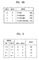
- FIG. 8A is an equivalent circuit diagram of the magnetic RAM 700 of FIG. 7.
- FIG. 8B is a table for explaining the states of data written to the magnetic RAM 700 of FIG. 7.
- the resistance-variable elements MTJ1 and MTJ2 have different resistances. If the resistance of the first resistance-variable element MTJ1 has a minimum value R1 and a maximum value of R1+ ⁇ R1, and the resistance value of the second resistance-variable element MTJ2 has a minimum value of R2 and a maximum value of R2+ ⁇ R2, the magnetic RAM 700 has four possible resistances according to data written to the first and second resistance-variable elements MTJ1 and MTJ2.
- the magnetic RAM 700 has a resistance of R1+R2 when all the two resistance-variable elements MTJ1 and MTJ2 store "0", has a resistance of R1+R2+ ⁇ R1 when only the first resistance-variable element MTJ1 stores "1”, has a resistance of R1+R2+ ⁇ R2 when only the second resistance-variable element MTJ2 stores data "1”, and has a resistance of R1+R2+ ⁇ R1+ ⁇ R2 when all the two resistance-variable elements MTJ1 and MTJ2 store "1".
- FIG. 9 is a table for explaining data written to the magnetic RAM 700 of FIG. 7.
- FIGS. 7 and 9 if currents flow in the right direction through the bit line BL and the second current supplying line CSL2, since the direction of a generated magnetic field is equal to the magnetization direction of the pinned ferromagnetic layers of the first and second resistance-variable elements MTJ1 and MTJ2, the total resistance of the first and second resistance-variable elements MTJ1 and MTJ2 decreases, thereby writing data "0" in the first and second resistance-variable elements MTJ1 and MTJ2.
- the magnetic RAM 700 can store 2-bit data using the two resistance-variable elements MTJ1 and MTJ2.
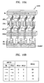
- FIG. 10A is a schematic view of a magnetic RAM 1000 in which the magnetization directions of pinned ferromagnetic layers of first and second resistance-variable elements MTJ1 and MTJ2 are different from those shown in FIG. 7.
- FIG. 10B is a table for explaining data written to the magnetic RAM 1000 of FIG. 10A.
- the magnetization directions of the pinned ferromagnetic layers of the first and second resistance-variable elements MTJ1 and MTJ2 are opposite to each other.
- the magnetization directions of the pinned ferromagnetic layers of the first and second resistance-variable element MTJ1 and MTJ2 are the same.
- a magnetic RAM includes an access transistor formed on a substrate, bit lines and digit lines alternately stacked on the access transistor, and a plurality of resistance-variable elements disposed between the bit lines and the digit lines, wherein the resistance-variable elements are electrically connected to each other.
- the bit lines include the bit lines BL and the second current supplying line CSL2 of the magnetic RAM 300 and 700 of FIGS. 3A and 7, respectively, and the digit lines include the first and third current supplying lines CSL1 and CSL3 in the magnetic RAMs 300 and 700 of FIGS. 3A and 7, respectively.
- the magnetic RAM according to an embodiment of the invention can have a similar structure to the magnetic RAMs 300 and 700 of FIGS. 3 and 7, and therefore, a detailed description thereof is omitted.
Landscapes
- Engineering & Computer Science (AREA)
- Computer Hardware Design (AREA)
- Chemical & Material Sciences (AREA)
- Nanotechnology (AREA)
- Physics & Mathematics (AREA)
- Mathematical Physics (AREA)
- Theoretical Computer Science (AREA)
- Crystallography & Structural Chemistry (AREA)
- Mram Or Spin Memory Techniques (AREA)
- Hall/Mr Elements (AREA)
- Semiconductor Memories (AREA)
Applications Claiming Priority (1)
| Application Number | Priority Date | Filing Date | Title |
|---|---|---|---|
| KR1020040086556A KR100604913B1 (ko) | 2004-10-28 | 2004-10-28 | 멀티 비트 셀 어레이 구조를 가지는 마그네틱 램 |
Publications (2)
| Publication Number | Publication Date |
|---|---|
| EP1653516A2 true EP1653516A2 (de) | 2006-05-03 |
| EP1653516A3 EP1653516A3 (de) | 2007-10-10 |
Family
ID=35258828
Family Applications (1)
| Application Number | Title | Priority Date | Filing Date |
|---|---|---|---|
| EP05023489A Withdrawn EP1653516A3 (de) | 2004-10-28 | 2005-10-27 | Magnetoresistiver Speicher mit wahlfreiem Zugriff |
Country Status (5)
| Country | Link |
|---|---|
| US (1) | US7463509B2 (de) |
| EP (1) | EP1653516A3 (de) |
| JP (1) | JP2006140468A (de) |
| KR (1) | KR100604913B1 (de) |
| CN (1) | CN100573713C (de) |
Cited By (3)
| Publication number | Priority date | Publication date | Assignee | Title |
|---|---|---|---|---|
| US7272028B2 (en) | 2005-05-27 | 2007-09-18 | Infineon Technologies Ag | MRAM cell with split conductive lines |
| CN101465407A (zh) * | 2007-12-21 | 2009-06-24 | 原子能委员会 | 热辅助磁写入存储器 |
| EP2466586A1 (de) * | 2010-12-16 | 2012-06-20 | Crocus Technology | Magnetische Multibit-Direktzugriffsspeicherzelle mit verbessertem Lesebereich |
Families Citing this family (25)
| Publication number | Priority date | Publication date | Assignee | Title |
|---|---|---|---|---|
| KR100695171B1 (ko) * | 2006-02-23 | 2007-03-14 | 삼성전자주식회사 | 마그네틱 도메인 이동을 이용하는 자기 메모리 장치 |
| KR100850508B1 (ko) * | 2006-08-04 | 2008-08-05 | 삼성전자주식회사 | 3차원적으로 배열된 메모리 셀 트랜지스터들을 구비하는낸드 플래시 메모리 장치 |
| US7697316B2 (en) * | 2006-12-07 | 2010-04-13 | Macronix International Co., Ltd. | Multi-level cell resistance random access memory with metal oxides |
| KR100814108B1 (ko) * | 2006-12-12 | 2008-03-14 | 인하대학교 산학협력단 | 자기터널접합을 이용한 논리회로 |
| KR100837412B1 (ko) * | 2006-12-12 | 2008-06-12 | 삼성전자주식회사 | 멀티 스택 메모리 소자 |
| KR100996191B1 (ko) | 2007-04-25 | 2010-11-24 | 주식회사 하이닉스반도체 | 비휘발성 메모리 소자 및 그 제조 방법 |
| KR101258268B1 (ko) * | 2007-07-26 | 2013-04-25 | 삼성전자주식회사 | 비휘발성 메모리 소자의 낸드형 저항성 메모리 셀 스트링들및 그 제조방법들 |
| KR100858688B1 (ko) * | 2007-12-06 | 2008-09-16 | 한양대학교 산학협력단 | 비휘발성 기억 장치 및 그 읽기 방법 |
| US7919794B2 (en) * | 2008-01-08 | 2011-04-05 | Qualcomm, Incorporated | Memory cell and method of forming a magnetic tunnel junction (MTJ) of a memory cell |
| US7804710B2 (en) * | 2008-03-31 | 2010-09-28 | International Business Machines Corporation | Multi-layer magnetic random access memory using spin-torque magnetic tunnel junctions and method for write state of the multi-layer magnetic random access memory |
| US8482966B2 (en) * | 2008-09-24 | 2013-07-09 | Qualcomm Incorporated | Magnetic element utilizing protective sidewall passivation |
| JP2010251529A (ja) * | 2009-04-16 | 2010-11-04 | Sony Corp | 半導体記憶装置およびその製造方法 |
| US8411494B2 (en) | 2009-07-21 | 2013-04-02 | Alexander Mikhailovich Shukh | Three-dimensional magnetic random access memory with high speed writing |
| US8331141B2 (en) | 2009-08-05 | 2012-12-11 | Alexander Mikhailovich Shukh | Multibit cell of magnetic random access memory with perpendicular magnetization |
| US8988934B2 (en) | 2010-07-27 | 2015-03-24 | Alexander Mikhailovich Shukh | Multibit cell of magnetic random access memory with perpendicular magnetization |
| JP5501277B2 (ja) * | 2011-03-24 | 2014-05-21 | 株式会社東芝 | 不揮発性記憶装置 |
| JP5537501B2 (ja) * | 2011-06-09 | 2014-07-02 | 株式会社東芝 | 半導体記憶装置およびその製造方法 |
| US8675390B2 (en) | 2011-10-21 | 2014-03-18 | Qualcomm Incorporated | System and method for MRAM having controlled averagable and isolatable voltage reference |
| US9203015B2 (en) | 2013-03-22 | 2015-12-01 | Hisanori Aikawa | Magnetic storage device |
| US8987846B2 (en) * | 2013-03-22 | 2015-03-24 | Yoshinori Kumura | Magnetic memory and manufacturing method thereof |
| CN103761987A (zh) * | 2014-01-08 | 2014-04-30 | 华中科技大学 | 一种基于阻性存储器的多位存储结构及其读写操作方法 |
| US9747967B2 (en) | 2014-09-26 | 2017-08-29 | Intel Corporation | Magnetic field-assisted memory operation |
| JP2017059740A (ja) * | 2015-09-18 | 2017-03-23 | 富士通株式会社 | 磁気トンネル接合素子及び半導体記憶装置 |
| JP2019160368A (ja) | 2018-03-13 | 2019-09-19 | 東芝メモリ株式会社 | 半導体記憶装置 |
| CN110277115B (zh) * | 2019-06-24 | 2021-01-01 | 中国科学院微电子研究所 | 基于磁隧道结的存储器及其读写方法、制作方法 |
Citations (7)
| Publication number | Priority date | Publication date | Assignee | Title |
|---|---|---|---|---|
| JP2001217398A (ja) | 2000-02-03 | 2001-08-10 | Rohm Co Ltd | 強磁性トンネル接合素子を用いた記憶装置 |
| US20020140060A1 (en) | 2001-03-29 | 2002-10-03 | Yoshiaki Asao | Semiconductor memory device using magneto resistive effect element |
| EP1321941A1 (de) | 2001-12-21 | 2003-06-25 | Kabushiki Kaisha Toshiba | MRAM mit gestapelten Speicherzellen |
| JP2004031640A (ja) | 2002-06-26 | 2004-01-29 | Toshiba Corp | 磁気メモリ装置 |
| US20040017639A1 (en) * | 2002-07-23 | 2004-01-29 | Deak James G. | High-stability low-offset-field double-tunnel-junction sensor |
| EP1398835A1 (de) | 2001-06-19 | 2004-03-17 | Matsushita Electric Industrial Co., Ltd. | Magnetspeicher und verfahren zu seiner ansteuerung und magnetspeichervorrichtung damit |
| US6795334B2 (en) * | 2001-12-21 | 2004-09-21 | Kabushiki Kaisha Toshiba | Magnetic random access memory |
Family Cites Families (13)
| Publication number | Priority date | Publication date | Assignee | Title |
|---|---|---|---|---|
| US5748519A (en) * | 1996-12-13 | 1998-05-05 | Motorola, Inc. | Method of selecting a memory cell in a magnetic random access memory device |
| JP3913971B2 (ja) | 1999-12-16 | 2007-05-09 | 株式会社東芝 | 磁気メモリ装置 |
| JP2002230965A (ja) * | 2001-01-24 | 2002-08-16 | Internatl Business Mach Corp <Ibm> | 不揮発性メモリ装置 |
| JP3527230B2 (ja) | 2001-06-19 | 2004-05-17 | 松下電器産業株式会社 | 磁気メモリの駆動方法 |
| JP3830785B2 (ja) | 2001-08-10 | 2006-10-11 | 田中貴金属工業株式会社 | Cvd用の有機ルテニウム化合物の製造方法及びcvd用の有機ルテニウム化合物 |
| JP2003133528A (ja) | 2001-10-24 | 2003-05-09 | Sony Corp | 情報記憶装置、その情報書き込み方法およびその製造方法 |
| KR100457159B1 (ko) * | 2001-12-26 | 2004-11-16 | 주식회사 하이닉스반도체 | 마그네틱 램 |
| JP3875568B2 (ja) * | 2002-02-05 | 2007-01-31 | 株式会社東芝 | 半導体装置及びその製造方法 |
| JP2003309251A (ja) * | 2002-04-18 | 2003-10-31 | Toshiba Corp | 磁気ランダムアクセスメモリ |
| US7042749B2 (en) | 2002-05-16 | 2006-05-09 | Micron Technology, Inc. | Stacked 1T-nmemory cell structure |
| US20050195673A1 (en) * | 2002-07-15 | 2005-09-08 | Yoshiaki Asao | Magnetic random access memory having memory cells configured by use of tunneling magnetoresistive elements |
| US6925003B2 (en) * | 2003-09-08 | 2005-08-02 | Hewlett-Packard Development Company, L.P. | Magnetic memory cell structure |
| US20050073878A1 (en) * | 2003-10-03 | 2005-04-07 | Taiwan Semiconductor Manufacturing Co., Ltd. | Multi-sensing level MRAM structure with different magnetoresistance ratios |
-
2004
- 2004-10-28 KR KR1020040086556A patent/KR100604913B1/ko not_active Expired - Lifetime
-
2005
- 2005-10-27 EP EP05023489A patent/EP1653516A3/de not_active Withdrawn
- 2005-10-27 JP JP2005313040A patent/JP2006140468A/ja active Pending
- 2005-10-27 US US11/260,602 patent/US7463509B2/en not_active Expired - Lifetime
- 2005-10-28 CN CNB2005100034564A patent/CN100573713C/zh not_active Expired - Lifetime
Patent Citations (7)
| Publication number | Priority date | Publication date | Assignee | Title |
|---|---|---|---|---|
| JP2001217398A (ja) | 2000-02-03 | 2001-08-10 | Rohm Co Ltd | 強磁性トンネル接合素子を用いた記憶装置 |
| US20020140060A1 (en) | 2001-03-29 | 2002-10-03 | Yoshiaki Asao | Semiconductor memory device using magneto resistive effect element |
| EP1398835A1 (de) | 2001-06-19 | 2004-03-17 | Matsushita Electric Industrial Co., Ltd. | Magnetspeicher und verfahren zu seiner ansteuerung und magnetspeichervorrichtung damit |
| EP1321941A1 (de) | 2001-12-21 | 2003-06-25 | Kabushiki Kaisha Toshiba | MRAM mit gestapelten Speicherzellen |
| US6795334B2 (en) * | 2001-12-21 | 2004-09-21 | Kabushiki Kaisha Toshiba | Magnetic random access memory |
| JP2004031640A (ja) | 2002-06-26 | 2004-01-29 | Toshiba Corp | 磁気メモリ装置 |
| US20040017639A1 (en) * | 2002-07-23 | 2004-01-29 | Deak James G. | High-stability low-offset-field double-tunnel-junction sensor |
Cited By (6)
| Publication number | Priority date | Publication date | Assignee | Title |
|---|---|---|---|---|
| US7272028B2 (en) | 2005-05-27 | 2007-09-18 | Infineon Technologies Ag | MRAM cell with split conductive lines |
| CN101465407A (zh) * | 2007-12-21 | 2009-06-24 | 原子能委员会 | 热辅助磁写入存储器 |
| EP2073210A1 (de) * | 2007-12-21 | 2009-06-24 | Commissariat a L'Energie Atomique | Magnetspeicher zum wärmeunterstützten Schreiben |
| FR2925747A1 (fr) * | 2007-12-21 | 2009-06-26 | Commissariat Energie Atomique | Memoire magnetique a ecriture assistee thermiquement |
| US7796428B2 (en) | 2007-12-21 | 2010-09-14 | Commissariat A L'energie Atomique | Thermally assisted magnetic write memory |
| EP2466586A1 (de) * | 2010-12-16 | 2012-06-20 | Crocus Technology | Magnetische Multibit-Direktzugriffsspeicherzelle mit verbessertem Lesebereich |
Also Published As
| Publication number | Publication date |
|---|---|
| CN100573713C (zh) | 2009-12-23 |
| JP2006140468A (ja) | 2006-06-01 |
| US7463509B2 (en) | 2008-12-09 |
| US20060092690A1 (en) | 2006-05-04 |
| KR100604913B1 (ko) | 2006-07-28 |
| CN1822226A (zh) | 2006-08-23 |
| KR20060037562A (ko) | 2006-05-03 |
| EP1653516A3 (de) | 2007-10-10 |
Similar Documents
| Publication | Publication Date | Title |
|---|---|---|
| US7463509B2 (en) | Magneto-resistive RAM having multi-bit cell array structure | |
| US8379429B2 (en) | Domain wall motion element and magnetic random access memory | |
| US7411815B2 (en) | Memory write circuit | |
| US7961509B2 (en) | Spin-transfer torque memory self-reference read and write assist methods | |
| US7286429B1 (en) | High speed sensing amplifier for an MRAM cell | |
| CN100466093C (zh) | 具有双隧道结的磁电阻存储器件 | |
| US8514605B2 (en) | MRAM diode array and access method | |
| KR100548997B1 (ko) | 다층박막구조의 자유층을 갖는 자기터널 접합 구조체들 및이를 채택하는 자기 램 셀들 | |
| US6477077B2 (en) | Non-volatile memory device | |
| US7859069B2 (en) | Magnetic storage element with storage layer magnetization directed for increased responsiveness to spin polarized current | |
| CN103280235A (zh) | 具有单独读取和写入路径的磁性隧道结装置 | |
| KR20050095914A (ko) | 자기 저항 메모리 셀, 자기 저항 메모리 셀의 매트릭스,자기 저항 메모리 셀의 매트릭스에 값을 기록하는 방법 및자기 저항 메모리 셀 제조 방법 | |
| KR20030048842A (ko) | 마그네틱 랜덤 엑세스 메모리 및 그 작동 방법 | |
| US8526215B2 (en) | Spatial correlation of reference cells in resistive memory array | |
| EP1509922B1 (de) | Mram-zelle und speicherarchitektur mit maximalem lesesignal und reduzierter elektromagnetischer interferenz | |
| KR20120050916A (ko) | 독립적으로 프로그래밍 가능한 자유 층 도메인들을 가지는 멀티-비트 자기 메모리 | |
| US7050326B2 (en) | Magnetic memory device with current carrying reference layer | |
| EP1473735A1 (de) | Magnetische Doppelübergangsspeicheranordnung und Leseverfahren | |
| US7257019B2 (en) | Systems and methods for a magnetic memory device that includes a single word line transistor | |
| US7352613B2 (en) | Magnetic memory device and methods for making a magnetic memory device | |
| US7203089B1 (en) | Systems and methods for a magnetic memory device that includes two word line transistors | |
| US7352614B2 (en) | Systems and methods for reading and writing a magnetic memory device | |
| KR20060012402A (ko) | 자기 메모리 장치 및 그의 구동방법 |
Legal Events
| Date | Code | Title | Description |
|---|---|---|---|
| PUAI | Public reference made under article 153(3) epc to a published international application that has entered the european phase |
Free format text: ORIGINAL CODE: 0009012 |
|
| AK | Designated contracting states |
Kind code of ref document: A2 Designated state(s): AT BE BG CH CY CZ DE DK EE ES FI FR GB GR HU IE IS IT LI LT LU LV MC NL PL PT RO SE SI SK TR |
|
| AX | Request for extension of the european patent |
Extension state: AL BA HR MK YU |
|
| PUAL | Search report despatched |
Free format text: ORIGINAL CODE: 0009013 |
|
| AK | Designated contracting states |
Kind code of ref document: A3 Designated state(s): AT BE BG CH CY CZ DE DK EE ES FI FR GB GR HU IE IS IT LI LT LU LV MC NL PL PT RO SE SI SK TR |
|
| AX | Request for extension of the european patent |
Extension state: AL BA HR MK YU |
|
| RIC1 | Information provided on ipc code assigned before grant |
Ipc: G11C 11/16 20060101ALI20070904BHEP Ipc: G11C 11/56 20060101ALI20070904BHEP Ipc: H01L 21/8247 20060101ALI20070904BHEP Ipc: H01L 27/22 20060101AFI20051115BHEP |
|
| 17P | Request for examination filed |
Effective date: 20080214 |
|
| 17Q | First examination report despatched |
Effective date: 20080327 |
|
| AKX | Designation fees paid |
Designated state(s): DE FR GB |
|
| R17C | First examination report despatched (corrected) |
Effective date: 20081002 |
|
| RAP1 | Party data changed (applicant data changed or rights of an application transferred) |
Owner name: SAMSUNG ELECTRONICS CO., LTD. |
|
| STAA | Information on the status of an ep patent application or granted ep patent |
Free format text: STATUS: THE APPLICATION IS DEEMED TO BE WITHDRAWN |
|
| 18D | Application deemed to be withdrawn |
Effective date: 20160518 |