EP1653517A2 - Dispositif d'affichage électroluminescent organique et son procédé de fabrication - Google Patents
Dispositif d'affichage électroluminescent organique et son procédé de fabrication Download PDFInfo
- Publication number
- EP1653517A2 EP1653517A2 EP05022911A EP05022911A EP1653517A2 EP 1653517 A2 EP1653517 A2 EP 1653517A2 EP 05022911 A EP05022911 A EP 05022911A EP 05022911 A EP05022911 A EP 05022911A EP 1653517 A2 EP1653517 A2 EP 1653517A2
- Authority
- EP
- European Patent Office
- Prior art keywords
- light shielding
- anode electrode
- display device
- light emitting
- organic
- Prior art date
- Legal status (The legal status is an assumption and is not a legal conclusion. Google has not performed a legal analysis and makes no representation as to the accuracy of the status listed.)
- Withdrawn
Links
Images






Classifications
-
- H—ELECTRICITY
- H05—ELECTRIC TECHNIQUES NOT OTHERWISE PROVIDED FOR
- H05B—ELECTRIC HEATING; ELECTRIC LIGHT SOURCES NOT OTHERWISE PROVIDED FOR; CIRCUIT ARRANGEMENTS FOR ELECTRIC LIGHT SOURCES, IN GENERAL
- H05B33/00—Electroluminescent light sources
- H05B33/12—Light sources with substantially two-dimensional [2D] radiating surfaces
- H05B33/22—Light sources with substantially two-dimensional [2D] radiating surfaces characterised by the chemical or physical composition or the arrangement of auxiliary dielectric or reflective layers
-
- H—ELECTRICITY
- H10—SEMICONDUCTOR DEVICES; ELECTRIC SOLID-STATE DEVICES NOT OTHERWISE PROVIDED FOR
- H10K—ORGANIC ELECTRIC SOLID-STATE DEVICES
- H10K59/00—Integrated devices, or assemblies of multiple devices, comprising at least one organic light-emitting element covered by group H10K50/00
- H10K59/80—Constructional details
- H10K59/805—Electrodes
- H10K59/8051—Anodes
- H10K59/80516—Anodes combined with auxiliary electrodes, e.g. ITO layer combined with metal lines
-
- H—ELECTRICITY
- H05—ELECTRIC TECHNIQUES NOT OTHERWISE PROVIDED FOR
- H05B—ELECTRIC HEATING; ELECTRIC LIGHT SOURCES NOT OTHERWISE PROVIDED FOR; CIRCUIT ARRANGEMENTS FOR ELECTRIC LIGHT SOURCES, IN GENERAL
- H05B33/00—Electroluminescent light sources
- H05B33/10—Apparatus or processes specially adapted to the manufacture of electroluminescent light sources
-
- H—ELECTRICITY
- H10—SEMICONDUCTOR DEVICES; ELECTRIC SOLID-STATE DEVICES NOT OTHERWISE PROVIDED FOR
- H10K—ORGANIC ELECTRIC SOLID-STATE DEVICES
- H10K50/00—Organic light-emitting devices
- H10K50/80—Constructional details
- H10K50/805—Electrodes
- H10K50/81—Anodes
- H10K50/814—Anodes combined with auxiliary electrodes, e.g. ITO layer combined with metal lines
-
- H—ELECTRICITY
- H10—SEMICONDUCTOR DEVICES; ELECTRIC SOLID-STATE DEVICES NOT OTHERWISE PROVIDED FOR
- H10K—ORGANIC ELECTRIC SOLID-STATE DEVICES
- H10K50/00—Organic light-emitting devices
- H10K50/80—Constructional details
- H10K50/86—Arrangements for improving contrast, e.g. preventing reflection of ambient light
-
- H—ELECTRICITY
- H10—SEMICONDUCTOR DEVICES; ELECTRIC SOLID-STATE DEVICES NOT OTHERWISE PROVIDED FOR
- H10K—ORGANIC ELECTRIC SOLID-STATE DEVICES
- H10K59/00—Integrated devices, or assemblies of multiple devices, comprising at least one organic light-emitting element covered by group H10K50/00
- H10K59/10—OLED displays
- H10K59/17—Passive-matrix OLED displays
-
- H—ELECTRICITY
- H10—SEMICONDUCTOR DEVICES; ELECTRIC SOLID-STATE DEVICES NOT OTHERWISE PROVIDED FOR
- H10K—ORGANIC ELECTRIC SOLID-STATE DEVICES
- H10K59/00—Integrated devices, or assemblies of multiple devices, comprising at least one organic light-emitting element covered by group H10K50/00
- H10K59/10—OLED displays
- H10K59/17—Passive-matrix OLED displays
- H10K59/173—Passive-matrix OLED displays comprising banks or shadow masks
-
- H—ELECTRICITY
- H10—SEMICONDUCTOR DEVICES; ELECTRIC SOLID-STATE DEVICES NOT OTHERWISE PROVIDED FOR
- H10K—ORGANIC ELECTRIC SOLID-STATE DEVICES
- H10K59/00—Integrated devices, or assemblies of multiple devices, comprising at least one organic light-emitting element covered by group H10K50/00
- H10K59/10—OLED displays
- H10K59/17—Passive-matrix OLED displays
- H10K59/179—Interconnections, e.g. wiring lines or terminals
-
- H—ELECTRICITY
- H10—SEMICONDUCTOR DEVICES; ELECTRIC SOLID-STATE DEVICES NOT OTHERWISE PROVIDED FOR
- H10K—ORGANIC ELECTRIC SOLID-STATE DEVICES
- H10K59/00—Integrated devices, or assemblies of multiple devices, comprising at least one organic light-emitting element covered by group H10K50/00
- H10K59/80—Constructional details
- H10K59/8791—Arrangements for improving contrast, e.g. preventing reflection of ambient light
-
- H—ELECTRICITY
- H10—SEMICONDUCTOR DEVICES; ELECTRIC SOLID-STATE DEVICES NOT OTHERWISE PROVIDED FOR
- H10K—ORGANIC ELECTRIC SOLID-STATE DEVICES
- H10K71/00—Manufacture or treatment specially adapted for the organic devices covered by this subclass
-
- H—ELECTRICITY
- H10—SEMICONDUCTOR DEVICES; ELECTRIC SOLID-STATE DEVICES NOT OTHERWISE PROVIDED FOR
- H10K—ORGANIC ELECTRIC SOLID-STATE DEVICES
- H10K71/00—Manufacture or treatment specially adapted for the organic devices covered by this subclass
- H10K71/10—Deposition of organic active material
- H10K71/12—Deposition of organic active material using liquid deposition, e.g. spin coating
Definitions
- the present invention relates to an organic electro luminescence display device and a fabricating method thereof, and more particularly to an organic electro luminescence display device that is adaptive for improving contrast ratio as well as improving the conductivity of an anode electrode, and a fabricating method thereof.
- the flat panel display device includes a liquid crystal display LCD, a field emission display FED, a plasma display panel PDP and an electro luminescence EL display device.
- the PDP is relatively simple in its structure and fabricating process, thus it is advantageous in being made into a large size screen but there is a disadvantage in that its light emitting efficiency and brightness is low and its power consumption is high.
- the LCD is mainly used for a display device of a notebook computer so that its demand increases, but there is a disadvantage in that it is difficult to be made into a large size screen and its power consumption is high. Further, the LCD has a disadvantage in that there is high light loss by optical display devices such as polarizing filter, prism sheet, diffusion sheet and so on and its viewing angle is narrow.
- the EL display device is largely divided into an inorganic EL and an organic EL and has an advantage in that the response speed is high and the light emitting efficiency, brightness and the viewing angle is high. Further, the organic EL display device might be able to display a picture with a high brightness of tens of thousands [cd/m 2 ] at a voltage of about 10[V].
- FIG. 1 is a perspective view representing a related art organic EL display device
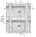
- FIG. 2 is a plane view specifically representing an A area of FIG. 1
- FIG. 3 is a sectional diagram of the organic EL display device taken along the lines I-I' and II-II'of FIG. 2.
- the organic El display device shown in FIGs. 1 to 3 is formed on a substrate 2 for an anode electrode 4 and a cathode electrode 12 to cross each other.
- a plurality of anode electrodes 4 are formed on the substrate 2 to be separated from each other with a designated gap.
- An opaque conductive pattern 5 is formed on one side of the anode electrode 4.
- the opaque conductive pattern 5 plays the role of improving the conductivity of the anode electrode 4 which is formed of a transparent conductive material such as ITO (indium tin oxide), IZO (indium zinc oxide), ITZO (indium tin zinc oxide) having high resistance.
- An insulating film 6 having an aperture ratio is formed in each EL cell (E) area on the substrate 2 where the anode electrode 4 and the opaque conductive pattern 5 are formed.
- a barrier rib 8 is located on the insulating film 6 for separating the organic light emitting layer 10 and the cathode electrode 12 which are to be formed thereon.
- the barrier rib 8 is formed in a direction of crossing the anode electrode 4 and has a reverse taper structure that an upper end part has a wide width than a lower end part.
- An organic light emitting layer 10 is formed on the insulating film 6 where the barrier rib 8 is formed, and the cathode electrode 12 is formed by depositing an electrode material on the entire surface.
- the organic light emitting layer 10 is formed by having a hole injection layer 10E, a hole transport layer 10D, a light emitting layer 10C, an electron transport layer 10B and an electron injection layer 10A deposited.
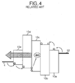
- the organic EL display device has electrons and holes emitted if a driving signal is applied to the anode electrode 4 and the cathode electrode 12, and the electron and hole emitted from the anode electrode 4 and the cathode electrode 12 are recombined within the light emitting layer 10C to generate a visible ray. At this moment, the generated visible ray exits to the outside through the anode electrode 4 to display a designated picture or image.
- the anode electrode 4 has a lower conductivity than the cathode electrode 12 which is formed of a metal of high conductivity such as aluminum AL even though the opaque conductive pattern 5 is formed for compensating the conductivity of the anode electrode 4, and the opaque conductive pattern 5 occupies part of a light emitting area P1 thus there is a problem in that the aperture ratio becomes smaller as much.
- the light incident from the outside almost completely transmits the anode electrode 4 and the organic light emitting layer 10.
- an external light 40 being incident from the surface of the substrate 2 transmits the organic light emitting layer 10 and the anode electrode 4 of a transparent conductive material and is reflected by the cathode electrode 12 of a metal electrode, as shown in FIG. 5. Accordingly, there is a problem in that the contrast ratio is deteriorated.
- an object of the present invention to provide an organic electro luminescence display device that is adaptive for improving the contrast ratio as well as improving the conductivity of an anode electrode, and a fabricating method thereof.
- an organic electro luminescence display device includes a plurality of anode electrodes which are disposed in parallel to a substrate, formed of a transparent conductive material and electrically separated from each other; a first conductive light shielding pattern formed along a first side of each of the anode electrodes; and a second conductive light shielding pattern formed along a second side of each of the anode electrodes.
- the first and second sides are parallel to each other, the first conductive light shielding pattern is formed to lay over the first side of the anode electrode, and the second conductive light shielding pattern is formed to lay over the second side of the anode electrode.
- the first and second conductive light shielding patterns have a remaining part in contact with the substrate except a part which lays over the anode electrode, so as to have a stepped section.
- the organic electro luminescence display device further includes an insulating film which partially exposes the anode electrode to define a light emitting area; an organic light emitting layer formed in the light emitting area; and a cathode electrode formed to cross the anode electrode with the organic light emitting layer therebetween, and wherein the insulating film is formed to cover the first and second conductive light shielding pattern.
- the first and second conductive light shielding patterns include an opaque conductive material and intercept an external light.
- a fabricating method of an organic electro luminescence display device includes the steps of: forming a plurality of anode electrodes which are disposed in parallel to a substrate, formed of a transparent conductive material and electrically separated from each other; and forming a first conductive light shielding pattern along a first side of each of the anode electrodes and a second conductive light shielding pattern along a second side of each of the anode electrodes.
- the first and second sides are parallel to each other, the first conductive light shielding pattern is formed to lay over the first side of the anode electrode, and the second conductive light shielding pattern is formed to lay over the second side of the anode electrode.
- the first and second conductive light shielding patterns have a remaining part in contact with the substrate except a part which lays over the anode electrode, so as to have a stepped section.
- the fabricating method further includes the steps of: forming an insulating film which partially exposes the anode electrode to define a light emitting area and covers the first and second conductive light shielding pattern; forming an organic light emitting layer in the light emitting area; and forming a cathode electrode to cross the anode electrode with the organic light emitting layer therebetween.
- the first and second conductive light shielding patterns include an opaque conductive material and intercept an external light.
- FIG. 1 a perspective view representing a related art organic electro luminescence display device
- FIG. 2 is a diagram specifically representing an A area of in FIG. 1;
- FIG. 3 is a sectional diagram of the organic electro luminescence display device taken along the lines I-I' and II-II' shown in FIG. 2;
- FIG. 4 is a diagram for explaining an light emitting principle of the related art organic electro luminescence display device
- FIG. 5 is a diagram representing that an incident external light is reflected at a cathode electrode of the organic electro luminescence display device
- FIG. 6 is a plane view specifically representing an area of an organic electro luminescence display device according to an embodiment of the present invention.
- FIG. 7 is a sectional diagram taken along the line III-III' shown in FIG. 6;
- FIG. 8 is a diagram specifically representing a shape of an opaque conductive pattern shown in FIGs. 6 and 7;
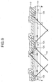
- FIG. 9 is a diagram representing a light shielding role of the opaque conductive pattern.
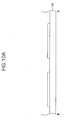
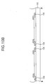
- FIGs. 10A to 10E are diagrams representing a fabricating method of the organic electro luminescence display device shown in FIG. 7.
- FIG. 6 is a plane view representing a part of an organic EL display device according to an embodiment of the present invention
- FIG. 7 is a sectional diagram illustrating the organic EL display device taken along the lines III-III' shown in FIG. 6.
- an organic EL display device includes an anode electrode 104 and a cathode electrode 112 formed to cross each other, and EL cells (E) formed for each intersection of the anode electrode 104 and the cathode electrode 112.
- a plurality of anode electrodes 104 are formed on the substrate 102 to be separated with a fixed gap, and the anode electrode 104 is formed of a transparent conductive material such as ITO, IZO, ITZO which has good light transmissivity and low conductivity.
- An opaque conductive pattern 105 is formed on a substrate 102 to be parallel to the anode electrode 102 and partially lay over both sides thereof, and the opaque conductive pattern 105 is formed to be covered by an insulating film 106.
- the opaque conductive pattern 105 is formed to lay over the both sides, i.e., left side (or first side) and right side (or second side), of the anode electrode 104. Accordingly, the conductivity of the anode electrode 104 is improved to increase its aperture ratio and contrast ratio.
- the opaque conductive patterns 105 are formed to lay over the both sides of the anode electrode 104 and have a wide line width, differently from the related art. Accordingly, the conductivity of the anode electrode 104 is improved in comparison with the related art.
- the opaque conductive pattern 105 is formed as an independent pattern so that the anode electrodes 104 are electrically insulated from each other.
- the opaque conductive pattern 105 is formed to lay over the anode electrode 104 and the other part is formed to extend to a non light emitting area P2 which does not overlap the anode electrode 104.
- the opaque conductive pattern 105 can be formed to be covered by the insulating film 106 which is formed in the non light emitting area P2. Accordingly, the opaque conductive pattern 105 is not located on the light emitting area P1 so that the overall aperture ratio can be improved, and the opaque conductive pattern 105 is mostly located in the non light emitting area P2 so that a significant amount of external light 140 can be intercepted in comparison with the related art as shown in FIG. 9, thereby improving the contrast ratio.
- the insulating film 106 formed to cover the opaque conductive pattern 105 is formed to have an aperture part which defines the light emitting area P1 for each EL cell (E) area.
- a barrier rib 108 for separating the cathode electrode 112 and an organic light emitting layer 110 which is to be formed thereon.
- the barrier rib 108 is formed in a direction of crossing the anode electrode 104 and has a reverse taper structure that an upper end part has a wider width than a lower end part.
- the organic light emitting layer 110 is formed on the insulating film 106 where the barrier rib 108 is formed and the cathode electrode 112 is formed by depositing an electrode material on the entire surface.
- the organic light emitting layer 110 is formed by having a hole injection layer 10E, a hole transport layer 10D, a light emitting layer 10C, an electron transport layer 10B and an electron injection layer 10A deposited in the same manner as the related art.
- the opaque conductive pattern 105 is formed to be parallel to the anode electrode 104 and to have its part lay over the both sides of the anode electrode 104, and is formed to be electrically separated from each other so that insulation is made between the anode electrodes 104. Accordingly, an area where the opaque conductive pattern 105 is formed becomes two times as big as the related art, thereby improving the conductivity of the anode electrode 104. Further, the opaque conductive pattern 105 is not located on the light emitting area P1, and at the same time, can be located at a significant part of the non light emitting area P2, thereby improving its contrast ratio and aperture ratio.
- FIGs. 10A to 10E are diagrams representing a fabricating method of the organic EL display device shown in FIG. 7, step by step.
- a transparent conductive material such as ITO, IZO, ITZO and so on is deposited on the substrate 102 by use of a deposition method such as sputtering, and then the transparent conductive material is patterned by a photolithography process and an etching process, thereby forming the anode electrode 104, as shown in FIG. 10A.
- An opaque conductive material such as molybdenum Mo is formed on the substrate 102 where the anode electrode 104 is formed, and then the opaque conductive material is patterned by the photolithography process and the etching process, thereby being electrically separated from each other and forming the opaque conductive pattern 105 to lay over the both sides, i.e., the left side (or first side) and right side (or second side), of the anode electrode 104, as shown in FIG 10B.
- a photo sensitive insulating material is coated by a spin-coating method over the substrate 102 where the opaque conductive pattern 105 is formed, and then the photo sensitive insulating material is patterned by the photolithography process, thereby exposing the light emitting area P1 and forming the insulating film 106 to cover the opaque conductive pattern 105, as shown in FIG. 10C.
- a photo sensitive organic material is deposited over the insulating material 106 and then the photo sensitive organic material is patterned by the photolithography process, thereby forming a barrier rib.
- the organic light emitting layer 110 is formed on the substrate 102 where the insulating film 106 and the barrier rib 108.
- a metal material such as aluminum Al is deposited on the substrate 102 where the organic light emitting layer 110, thereby forming the cathode electrode 112, as shown in FIG. 10E.
- the opaque conductive pattern which is parallel to the anode electrode and lays over the both sides (the left side and the right side) of the anode electrode and which is electrically separated from each other for insulation to be made between the anode electrodes. Accordingly, the area where the opaque conductive pattern is to be formed becomes twice as big as the related art, thereby improving the conductivity of the anode electrode. Further, the opaque conductive pattern is not located on the light emitting area, and at the same time, is located at a significant part of the non light emitting area, thereby improving the aperture ratio and the contrast ratio at the same time.
Landscapes
- Physics & Mathematics (AREA)
- Optics & Photonics (AREA)
- Engineering & Computer Science (AREA)
- Manufacturing & Machinery (AREA)
- Electroluminescent Light Sources (AREA)
- Devices For Indicating Variable Information By Combining Individual Elements (AREA)
Applications Claiming Priority (1)
| Application Number | Priority Date | Filing Date | Title |
|---|---|---|---|
| KR1020040087215A KR100692865B1 (ko) | 2004-10-29 | 2004-10-29 | 유기 전계발광표시소자 및 그 제조방법 |
Publications (2)
| Publication Number | Publication Date |
|---|---|
| EP1653517A2 true EP1653517A2 (fr) | 2006-05-03 |
| EP1653517A3 EP1653517A3 (fr) | 2007-10-24 |
Family
ID=35458224
Family Applications (1)
| Application Number | Title | Priority Date | Filing Date |
|---|---|---|---|
| EP05022911A Withdrawn EP1653517A3 (fr) | 2004-10-29 | 2005-10-20 | Dispositif d'affichage électroluminescent organique et son procédé de fabrication |
Country Status (5)
| Country | Link |
|---|---|
| US (1) | US7868330B2 (fr) |
| EP (1) | EP1653517A3 (fr) |
| JP (1) | JP2006128110A (fr) |
| KR (1) | KR100692865B1 (fr) |
| CN (1) | CN1773718A (fr) |
Cited By (2)
| Publication number | Priority date | Publication date | Assignee | Title |
|---|---|---|---|---|
| DE102008021655A1 (de) * | 2008-04-30 | 2009-11-12 | Saint-Gobain Sekurit Deutschland Gmbh & Co. Kg | Substrat, Strahlungsquelle, Photozelle und Herstellungsverfahren |
| WO2015192479A1 (fr) * | 2014-06-17 | 2015-12-23 | 京东方科技集团股份有限公司 | Écran d'affichage à diodes électroluminescentes organiques et son procédé de préparation, et masque |
Families Citing this family (8)
| Publication number | Priority date | Publication date | Assignee | Title |
|---|---|---|---|---|
| JP2008135318A (ja) * | 2006-11-29 | 2008-06-12 | Toppan Printing Co Ltd | 有機エレクトロルミネッセンス素子およびその製造方法 |
| JP5455230B2 (ja) * | 2010-05-25 | 2014-03-26 | Necライティング株式会社 | 有機エレクトロルミネッセンス照明装置の製造方法 |
| JP2012043583A (ja) | 2010-08-17 | 2012-03-01 | Sony Corp | 表示装置およびその製造方法 |
| KR20120119091A (ko) * | 2011-04-20 | 2012-10-30 | 삼성디스플레이 주식회사 | 유기 발광 표시 장치와, 이의 제조 방법 |
| WO2013047621A1 (fr) * | 2011-09-30 | 2013-04-04 | シャープ株式会社 | Dispositif d'affichage et son procédé de fabrication |
| JPWO2013190636A1 (ja) * | 2012-06-19 | 2016-02-08 | パイオニア株式会社 | 有機elパネル |
| CN111155055A (zh) * | 2020-01-06 | 2020-05-15 | 武汉华星光电半导体显示技术有限公司 | Oled面板、其蒸镀方法和其掩膜版组 |
| KR102935577B1 (ko) * | 2020-01-16 | 2026-03-06 | 삼성디스플레이 주식회사 | 디스플레이 장치 |
Citations (6)
| Publication number | Priority date | Publication date | Assignee | Title |
|---|---|---|---|---|
| EP0891122A1 (fr) | 1997-07-09 | 1999-01-13 | TDK Corporation | Dispositif organique électroluminescent |
| GB2329506A (en) | 1997-09-22 | 1999-03-24 | Fuji Electric Co Ltd | Organic light-emitting device |
| EP1107335A2 (fr) | 1999-11-30 | 2001-06-13 | TDK Corporation | Dispositif d'affichage électroluminescent organique |
| US20010024083A1 (en) | 2000-03-27 | 2001-09-27 | Semiconductor Energy Laboratory Co., Ltd | Light emitting apparatus and method of manufacturing the same |
| WO2003075616A1 (fr) | 2002-03-04 | 2003-09-12 | Rohm Co., Ltd. | Ecran electroluminescent organique comprenant un separateur d'electrodes, et procede de fabrication |
| US20040140760A1 (en) | 2002-10-25 | 2004-07-22 | Ritdisplay Corporation | Silver alloy used in an organic electroluminescent panel |
Family Cites Families (4)
| Publication number | Priority date | Publication date | Assignee | Title |
|---|---|---|---|---|
| US6037005A (en) * | 1998-05-12 | 2000-03-14 | 3M Innovative Properties Company | Display substrate electrodes with auxiliary metal layers for enhanced conductivity |
| JP4693262B2 (ja) | 2000-03-27 | 2011-06-01 | 株式会社半導体エネルギー研究所 | パッシブマトリクス型の発光装置 |
| EP1386359A1 (fr) * | 2001-04-26 | 2004-02-04 | Koninklijke Philips Electronics N.V. | Dispositif electroluminescent et procede de fabrication de ce dernier |
| DE10133684A1 (de) * | 2001-07-11 | 2003-02-13 | Osram Opto Semiconductors Gmbh | Organisches, farbiges, elektrolumineszierendes Display und dessen Herstellung |
-
2004
- 2004-10-29 KR KR1020040087215A patent/KR100692865B1/ko not_active Expired - Fee Related
-
2005
- 2005-10-20 EP EP05022911A patent/EP1653517A3/fr not_active Withdrawn
- 2005-10-26 US US11/258,168 patent/US7868330B2/en active Active
- 2005-10-26 JP JP2005311709A patent/JP2006128110A/ja active Pending
- 2005-10-28 CN CNA2005101184770A patent/CN1773718A/zh active Pending
Patent Citations (6)
| Publication number | Priority date | Publication date | Assignee | Title |
|---|---|---|---|---|
| EP0891122A1 (fr) | 1997-07-09 | 1999-01-13 | TDK Corporation | Dispositif organique électroluminescent |
| GB2329506A (en) | 1997-09-22 | 1999-03-24 | Fuji Electric Co Ltd | Organic light-emitting device |
| EP1107335A2 (fr) | 1999-11-30 | 2001-06-13 | TDK Corporation | Dispositif d'affichage électroluminescent organique |
| US20010024083A1 (en) | 2000-03-27 | 2001-09-27 | Semiconductor Energy Laboratory Co., Ltd | Light emitting apparatus and method of manufacturing the same |
| WO2003075616A1 (fr) | 2002-03-04 | 2003-09-12 | Rohm Co., Ltd. | Ecran electroluminescent organique comprenant un separateur d'electrodes, et procede de fabrication |
| US20040140760A1 (en) | 2002-10-25 | 2004-07-22 | Ritdisplay Corporation | Silver alloy used in an organic electroluminescent panel |
Cited By (4)
| Publication number | Priority date | Publication date | Assignee | Title |
|---|---|---|---|---|
| DE102008021655A1 (de) * | 2008-04-30 | 2009-11-12 | Saint-Gobain Sekurit Deutschland Gmbh & Co. Kg | Substrat, Strahlungsquelle, Photozelle und Herstellungsverfahren |
| DE102008021655B4 (de) * | 2008-04-30 | 2012-06-06 | Saint-Gobain Sekurit Deutschland Gmbh & Co. Kg | Strahlungsquelle und Solarzelle |
| WO2015192479A1 (fr) * | 2014-06-17 | 2015-12-23 | 京东方科技集团股份有限公司 | Écran d'affichage à diodes électroluminescentes organiques et son procédé de préparation, et masque |
| US9818970B2 (en) | 2014-06-17 | 2017-11-14 | Boe Technology Group Co., Ltd. | Organic light emitting diode display panel, manufacturing method thereof and mask plate |
Also Published As
| Publication number | Publication date |
|---|---|
| EP1653517A3 (fr) | 2007-10-24 |
| CN1773718A (zh) | 2006-05-17 |
| US7868330B2 (en) | 2011-01-11 |
| KR20060038067A (ko) | 2006-05-03 |
| US20060091381A1 (en) | 2006-05-04 |
| JP2006128110A (ja) | 2006-05-18 |
| KR100692865B1 (ko) | 2007-03-09 |
Similar Documents
| Publication | Publication Date | Title |
|---|---|---|
| CN110321026B (zh) | 用于具有改进的视角均匀性的显示器的触摸传感器 | |
| CN109950290B (zh) | Amoled显示屏、显示设备及移动终端 | |
| US9515129B2 (en) | Organic light emitting display apparatus and manufacturing method thereof | |
| EP2991121B1 (fr) | Substrat de matrice, procédé de fabrication de substrat de matrice et dispositif d'affichage | |
| US7868330B2 (en) | Organic electro-luminescence display device and fabricating method thereof | |
| KR20230099767A (ko) | 표시 장치 | |
| CN120583867B (zh) | 显示面板、显示面板的制备方法以及显示装置 | |
| JP5089867B2 (ja) | 有機電界発光表示素子及びその製造方法 | |
| KR20150075668A (ko) | 유기전계발광 표시장치 및 그 제조 방법 | |
| US7567029B2 (en) | Organic electro-luminescence display device and fabricating method thereof | |
| KR100705270B1 (ko) | 유기 전계 발광 표시장치 및 그 제조방법 | |
| KR100692051B1 (ko) | 유기 전계발광표시장치 및 그 제조방법 | |
| US20250359467A1 (en) | Display device and method of manufacturing the same | |
| KR100556697B1 (ko) | 유기 전계 발광 소자 및 그 제조방법 | |
| EP1657762A1 (fr) | Dispositif d'affichage électroluminescent organique et méthode de fabrication celle-ci | |
| KR100638145B1 (ko) | 유기 전계발광 표시소자 및 그 제조방법 | |
| KR100592390B1 (ko) | 유기 전계 발광 표시장치 및 그 제조방법 | |
| US12333117B2 (en) | Touch structure, display panel and touch display device | |
| KR100717332B1 (ko) | 유기 전계발광표시소자 및 그 제조방법 | |
| KR100667357B1 (ko) | 유기 전계발광 표시소자 및 그 제조방법 | |
| KR100739580B1 (ko) | 유기 발광 표시 장치 | |
| KR100696440B1 (ko) | 유기 전계발광 표시소자 및 그 제조방법 | |
| KR100638143B1 (ko) | 유기 전계발광 표시소자 및 그 제조방법 | |
| KR100638144B1 (ko) | 유기 전계발광 표시소자 및 그 제조방법 | |
| KR100625034B1 (ko) | 유기 전계발광표시소자 및 그 제조방법 |
Legal Events
| Date | Code | Title | Description |
|---|---|---|---|
| PUAI | Public reference made under article 153(3) epc to a published international application that has entered the european phase |
Free format text: ORIGINAL CODE: 0009012 |
|
| 17P | Request for examination filed |
Effective date: 20051020 |
|
| AK | Designated contracting states |
Kind code of ref document: A2 Designated state(s): AT BE BG CH CY CZ DE DK EE ES FI FR GB GR HU IE IS IT LI LT LU LV MC NL PL PT RO SE SI SK TR |
|
| AX | Request for extension of the european patent |
Extension state: AL BA HR MK YU |
|
| PUAL | Search report despatched |
Free format text: ORIGINAL CODE: 0009013 |
|
| AK | Designated contracting states |
Kind code of ref document: A3 Designated state(s): AT BE BG CH CY CZ DE DK EE ES FI FR GB GR HU IE IS IT LI LT LU LV MC NL PL PT RO SE SI SK TR |
|
| AX | Request for extension of the european patent |
Extension state: AL BA HR MK YU |
|
| RIC1 | Information provided on ipc code assigned before grant |
Ipc: H01L 51/56 20060101ALN20070918BHEP Ipc: H01L 27/32 20060101ALI20070918BHEP Ipc: H01L 51/52 20060101AFI20070918BHEP |
|
| 17Q | First examination report despatched |
Effective date: 20080523 |
|
| AKX | Designation fees paid |
Designated state(s): DE FR GB |
|
| STAA | Information on the status of an ep patent application or granted ep patent |
Free format text: STATUS: THE APPLICATION IS DEEMED TO BE WITHDRAWN |
|
| 18D | Application deemed to be withdrawn |
Effective date: 20121211 |