EP1653621A2 - Commutateur optique à touche tactile - Google Patents
Commutateur optique à touche tactile Download PDFInfo
- Publication number
- EP1653621A2 EP1653621A2 EP05021757A EP05021757A EP1653621A2 EP 1653621 A2 EP1653621 A2 EP 1653621A2 EP 05021757 A EP05021757 A EP 05021757A EP 05021757 A EP05021757 A EP 05021757A EP 1653621 A2 EP1653621 A2 EP 1653621A2
- Authority
- EP
- European Patent Office
- Prior art keywords
- light
- carrier
- touch switch
- optical touch
- recess
- Prior art date
- Legal status (The legal status is an assumption and is not a legal conclusion. Google has not performed a legal analysis and makes no representation as to the accuracy of the status listed.)
- Granted
Links
- 230000003287 optical effect Effects 0.000 title claims abstract description 18
- 239000002241 glass-ceramic Substances 0.000 claims description 18
- 230000004888 barrier function Effects 0.000 claims description 2
- 230000000873 masking effect Effects 0.000 abstract 1
- 238000010438 heat treatment Methods 0.000 description 4
- 230000001960 triggered effect Effects 0.000 description 4
- 239000000463 material Substances 0.000 description 2
- 238000000034 method Methods 0.000 description 2
- 230000011514 reflex Effects 0.000 description 2
- RYGMFSIKBFXOCR-UHFFFAOYSA-N Copper Chemical compound [Cu] RYGMFSIKBFXOCR-UHFFFAOYSA-N 0.000 description 1
- ATJFFYVFTNAWJD-UHFFFAOYSA-N Tin Chemical compound [Sn] ATJFFYVFTNAWJD-UHFFFAOYSA-N 0.000 description 1
- 238000005452 bending Methods 0.000 description 1
- 230000005540 biological transmission Effects 0.000 description 1
- 239000000969 carrier Substances 0.000 description 1
- 239000004020 conductor Substances 0.000 description 1
- 229910052802 copper Inorganic materials 0.000 description 1
- 239000010949 copper Substances 0.000 description 1
- 230000005283 ground state Effects 0.000 description 1
- 238000009434 installation Methods 0.000 description 1
- 238000012423 maintenance Methods 0.000 description 1
- 238000004519 manufacturing process Methods 0.000 description 1
- 238000005192 partition Methods 0.000 description 1
- 230000001681 protective effect Effects 0.000 description 1
- 230000005855 radiation Effects 0.000 description 1
- 230000007704 transition Effects 0.000 description 1
- 238000011144 upstream manufacturing Methods 0.000 description 1
- 239000013598 vector Substances 0.000 description 1
- 230000003313 weakening effect Effects 0.000 description 1
Images

Classifications
-
- H—ELECTRICITY
- H03—ELECTRONIC CIRCUITRY
- H03K—PULSE TECHNIQUE
- H03K17/00—Electronic switching or gating, i.e. not by contact-making and –breaking
- H03K17/94—Electronic switching or gating, i.e. not by contact-making and –breaking characterised by the way in which the control signals are generated
- H03K17/96—Touch switches
- H03K17/9627—Optical touch switches
- H03K17/9631—Optical touch switches using a light source as part of the switch
Definitions
- the invention relates to an optical touch switch, in particular for an at least partially translucent glass ceramic hob, with at least one light transmitter and / or a light receiver on or in at least one or a common carrier.
- Such a device is known from EP 0 766 887 B1.
- a self-illuminating optical touch switch is described with a light source whose emitted light is collimated with a lens system and then focused on at least one focal point. At the focal point, the light hits a transparent surface. If the transparent surface is covered on the side facing away from the light source, the light is reflected back in the direction of the lens system. This changes the beam path of the reflected light so that the light is directed to a detector, the incident light and detects its intensity and generates a corresponding signal.
- the disadvantage of this arrangement the complex and costly structure that results from the lens system and its necessary exact installation.
- the object of the invention is therefore to provide a touch switch of the type mentioned, which overcomes the disadvantages of the prior art and in particular allows a simplification of its structure.
- the light signal emanating from the light emitter and / or the light signal to be received by the light receiver is delimited by at least one mask-like section of the carrier with at least one recess and / or one divider.
- the carrier may be a largely flat body with a small height extent, in which the at least one recess is arranged, for example, a support for electrical and / or electronic components such as a printed circuit board or the like.
- the at least one recess may have at least partially parallel flanks, by which the light signal emanating from the light transmitter is limited laterally. Also by the at least one or a further recess of the receiving range of the light receiver is limited, which can be approximately limited to a point, but at least limited to a certain area.
- the light is limited by the recess whose individual light beams can be aligned approximately to the main transmitter direction of the light emitter.
- the recesses preferably have a clear width of up to 10 mm, preferably a clear width of 1 mm to 3 mm.
- a switching operation of the touch switch is triggered by light from the light emitter entering the reception area of the light receiver. It does not matter whether the light emitter and the light receiver are arranged on one or more carriers, wherein an arrangement on a carrier is simpler.
- a separating device preferably a separating web or a partition, may be provided to avoid stray light between the transmitter and the receiver. If this is arranged between the light emitter and the light receivers, it is advantageous if their dimensions exceed the height expansions of at least the transmitter or the receiver, in particular also in the direction away from the cover. A smaller dimensioning is sufficient if the separating web is provided only between the beam path and the receiving area.
- a further optics or beam path limitation which is introduced into the beam path of the light emitter or light receiver or upstream of this, so it can be dispensed with.
- the touch switch as a reflection light barrier with a light emitter, preferably a light emitting diode, short LED, and a light receiver, preferably phototransistor, a pin diode or a light-sensitive resistor is formed.
- the main emission direction of the light emitter, or the main reception direction of the light receiver is aligned with the respective mask-like section of the carrier assigned to the touch switch.
- the light signals strike a contact surface at which the signals are at least partially reflected in the direction of the light receiver. This responds to the light and initiates a switching signal.
- the touch switch on the underside of the hob or arranged below.
- the carrier of the light emitter and the light receiver is oriented such that their main end and main reception directions are through the hob.
- the light emitted by the light emitter can then emerge in a ground state at least to a large extent through the hob.
- the article may be, for example, a finger of an operator.
- the carrier By aligning the main emission direction of the light emitter and the main receiving direction of the light receiver on the respective, the touch switch associated, mask-like portion of the carrier, the carrier can serve as a substitute for additional optics, such as a light beam shield as in previous touch switches.
- Light emitters and light receivers can be aligned so that the vectors of their Hauptabstrahl- and main reception directions on the hob surface are only a small distance from each other or preferably intersect.
- the opening angles of the main radiation area and the main reception area are advantageously approximately equal.
- the light beam is an undirected light beam.
- the carrier is designed as a component carrier, in particular as a printed circuit board, and has an assembly side for receiving components.
- a carrier can also accommodate other components in addition to the components for the touch switch, which serve, for example, the control of a glass ceramic cooktop.
- the printed circuit board Due to the one-sided assembly of the printed circuit board, the printed circuit board on a largely flat upper side. With this, it can be applied to surfaces which are preferably designed to be electrically insulating, without having to provide protective devices for the electronic components mounted on the printed circuit board.
- a surface may be the underside of a cover, such as a glass ceramic hob, against which the top of the circuit board may rest.
- the carrier lies at least partially with one side on an underside of a cover.
- the abutting side of the carrier is the side opposite to the component side.
- the light transmitter and the light receiver are provided on the component side. Since the known from the prior art Lichtstrahlableungen can be omitted, resulting in a very compact design of Bermmschalters whose height is composed only of the height of the circuit board and the height of the components on the circuit board.
- light transmitters and / or light receivers are partially fixed in, preferably at least directly to, the at least one recess in the carrier.
- the recesses can be used as a replacement for, for example, an additional tube for laterally delimiting the beam path.
- the flanks of the recesses in the carrier are coated or reflective. This can be advantageously carried out in the manufacture of the circuit board.
- This is preferably realized with a reflective layer, which in particular comprises copper or, even better, tin.
- the layer may also be designed as a sleeve which can be introduced into the recess, preferably pressed. Due to the reflective layer in the recesses, not all the scattered light is shielded from the carrier, but also hits the light receiver. This increases the intensity of the beam.
- the reflective layer is used to collect incident light rays, so that even those rays are directed to the light receiver, which are not reflected at an exact angle from the surface of the hob.
- the carrier has a thickness of up to 5 mm, which is preferably between 1.0 mm and 2.0 mm.
- the light beam and the area which can be monitored by the light receiver can be brought to an optimum size with a size of 1 mm to 5 mm, given a corresponding size of the recess.
- the mask-like recess in the carrier preferably the part of the recess above the light emitter, as a display device, preferably as a symbol formed.
- a display device preferably as a symbol formed.
- the display device may be designed differently, so that a pictogram of a device to be operated of an electrical appliance, such as a radiant heater of a glass ceramic cooktop, can be displayed.
- a number, a letter, a word or combinations thereof are possible.
- the symbol is represented as a recess through which the light beam is guided, or as a mask or surface which shadows an area in the beam path.
- a display device is provided as a multi-segment display on the carrier, in particular as a seven-segment display, which projects at least partially from the component side of the carrier into a recess in the carrier, so that the main emission direction of the seven-segment display essentially corresponds to the main emission direction of the transmission device ,
- the seven-segment display can be used, for example, to indicate energy delivery levels of the radiators, temperatures or, for example, the time. Due to the fact that the display projects at least partially from the component side of the carrier into a recess in the carrier, the carrier designed as a printed circuit board can continue to have only one component side.
- any type of display can be used, for example, a display.
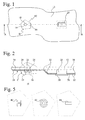
- FIG. 1 shows an optical touch switch 10 according to the invention, which is arranged under a glass ceramic hob 12.
- the light transmitter 14 and the light receiver 16 is indicated to recognize. These are arranged forming a gap.
- the light emitted by the light emitter 14, when using a light emitter that emits light in the visible wavelength range, can be perceived on the surface of the glass ceramic hob 12 as a light circle 18. Preferably, however, light of a non-visible wavelength is taken.
- a seven-segment display 20 is arranged as a display device. It can be used, for example, to display a selected by a user energy delivery level of a heating element, not shown, which is also arranged in the glass ceramic hob 12.
- FIG. 2 likewise shows the arrangement of the optical touch switch 10 with the light transmitter 14 and the light receiver 16.
- Light transmitter 14 and light receiver 16 are mounted on a component side 24 of a component carrier 22, preferably soldered to corresponding conductor tracks, which is designed as a printed circuit board.
- 22 recesses 26 are provided in the circuit board, on the one hand limit the propagation of the light emitted by the light emitter 14 and on the other limit the range from which can be made to the light receiver 16 perceptible light to the light receiver 16.
- the flanks of the recesses 26 are coated with a reflective layer 28, which may consist of any type of reflective material.
- the seven-segment display 20 is coming from the assembly side 24 of the circuit board 22 so inserted through a further recess in the circuit board 22 that a collar 30, which is part of the seven-segment display 20, abuts the component side 24 of the circuit board. On the collar 30 contacts, not shown, are provided for transmitting electrical signals to the seven-segment display.
- an intermediate space or distance is provided between the light transmitter 14 and the light receiver 16 and the at least one seven-segment display 20.
- the circuit board 22 and the seven-segment display 20 both of which at least partially rest against the underside of the glass ceramic hob 12
- mutual recesses and / or material weakenings are formed in the circuit board.
- the circuit board 22 is thus executed bent so that different height expansions of the different components can be compensated.
- the sides where the grooves 32 are inserted are the component side 24 and the side opposite to the component side 24.
- the circuit board 22 is weakened so that it can be deformed without being destroyed.
- the offset in the printed circuit board which divides it into a top printed circuit board section 34 and a bottom printed circuit board section 36, is disposed between the optical touch switch 10 and the seven-segment display 20 in the embodiment of the invention described herein.
- FIG. 3 shows the unactuated state of the touch switch 10.
- the light beams 46 emitted by the light emitter 14 pass through the recess 26 in the printed circuit board 22 partially unhindered.
- Light rays, which emerge obliquely from the light emitter, are reflected at the reflection layer 28, which covers the flank of the recess 26. This results in a region 54 in the illuminated area, to which an increased number of light beams 46 strikes.
- the light beams 46 In order for the light beams 46 to reach the light receiver 16, they must be reflected on the surface 56 of the glass-ceramic cooktop 12. This happens when an area or the area 54 is covered by an object, for example a finger 48, in particular by direct placement on the top side of the glass-ceramic cooktop 12.
- the light 46 is largely reflected undirected in the region 54.
- this is illustrated by the light beam 50 which runs along the center beam 50.
- the light beam 50 passes through the recess 26 in the circuit board 22 and thus passes through reflection on the underside of the finger in the region 54 to the light receiver 16.
- parts of the reflected light beam 50 at the reflection layer 28 are reflected in the direction of the light receiver 16, which is not shown, but is obvious.
- the emitted light beam shown on the far left in FIGS. 3 and 4 does not become or hardly reflected, since in his incidence on the glass ceramic hob 12 of the fingers 48 is not placed. Suffers a sufficient amount of light on the light receiver 16, this is a corresponding signal to an unillustrated control electronics on.
- the light receiver may be set such that it reacts only to light of a specific wavelength, which is then emitted by the light transmitter 14 and preferably lies in the non-visible wavelength range.
- FIG. 5 shows exemplary symbols 40, 42, 44.
- a symbol H may be embodied as a letter 40, as a symbol for a heating element 42, or as a mathematical symbol 44, such as a plus or a minus symbol. It is also conceivable that the symbol when using a plurality of heating elements, the position of the heating element, which is actuated with the optical touch switch 10.
Landscapes
- Switches Operated By Changes In Physical Conditions (AREA)
- Electronic Switches (AREA)
Applications Claiming Priority (1)
| Application Number | Priority Date | Filing Date | Title |
|---|---|---|---|
| DE102004053496A DE102004053496A1 (de) | 2004-10-28 | 2004-10-28 | Optischer Berührschalter |
Publications (3)
| Publication Number | Publication Date |
|---|---|
| EP1653621A2 true EP1653621A2 (fr) | 2006-05-03 |
| EP1653621A3 EP1653621A3 (fr) | 2008-01-09 |
| EP1653621B1 EP1653621B1 (fr) | 2009-12-23 |
Family
ID=35789216
Family Applications (1)
| Application Number | Title | Priority Date | Filing Date |
|---|---|---|---|
| EP05021757A Expired - Lifetime EP1653621B1 (fr) | 2004-10-28 | 2005-10-06 | Commutateur optique à touche tactile |
Country Status (4)
| Country | Link |
|---|---|
| EP (1) | EP1653621B1 (fr) |
| AT (1) | ATE453248T1 (fr) |
| DE (2) | DE102004053496A1 (fr) |
| ES (1) | ES2338793T3 (fr) |
Cited By (2)
| Publication number | Priority date | Publication date | Assignee | Title |
|---|---|---|---|---|
| EP1944552A3 (fr) * | 2007-01-03 | 2009-04-15 | SELTA S.r.l. | Tableau supérieur de commande de cuisson et affichages alphanumériques intégrés à celui-ci |
| US7786425B2 (en) | 2006-12-15 | 2010-08-31 | Diehl Ako Stiftung & Co. Kg | Optical sensor |
Families Citing this family (4)
| Publication number | Priority date | Publication date | Assignee | Title |
|---|---|---|---|---|
| DE102007060293A1 (de) | 2007-12-12 | 2009-06-18 | Diehl Ako Stiftung & Co. Kg | Berührungsempfindlicher Tastschalter |
| DE102010062428B4 (de) | 2010-12-03 | 2013-11-21 | BSH Bosch und Siemens Hausgeräte GmbH | Optische Bedien- und/oder Anzeigeeinheit |
| DE102012200292A1 (de) * | 2012-01-11 | 2013-07-11 | BSH Bosch und Siemens Hausgeräte GmbH | Bedieneinrichtung für ein Haushaltsgerät sowie Haushaltsgerät mit einer derartigen Bedieneinrichtung |
| DE102012217197B4 (de) * | 2012-09-24 | 2025-08-21 | Ifm Electronic Gmbh | Optischer Näherungsschalter |
Citations (4)
| Publication number | Priority date | Publication date | Assignee | Title |
|---|---|---|---|---|
| DE2936815A1 (de) | 1979-09-12 | 1981-04-02 | Vereinigte Glaswerke Gmbh, 5100 Aachen | Schalttafel mit beruehrungsschaltern |
| EP0446642A1 (fr) | 1990-03-13 | 1991-09-18 | Gaggenau-Werke Haus- und Lufttechnik GmbH | Dispositif pour mettre en circuit des installations électriques |
| EP0766887B1 (fr) | 1994-06-21 | 1999-03-31 | United Technologies Corporation | Interrupteur optique a effleurement auto-eclairant |
| DE20008425U1 (de) | 2000-05-10 | 2001-09-13 | Diehl Controls Nürnberg GmbH & Co. KG, 90451 Nürnberg | Berührungssensitive Steuerungsbaugruppe |
Family Cites Families (7)
| Publication number | Priority date | Publication date | Assignee | Title |
|---|---|---|---|---|
| US3621268A (en) * | 1967-12-19 | 1971-11-16 | Int Standard Electric Corp | Reflection type contactless touch switch having housing with light entrance and exit apertures opposite and facing |
| GB1471357A (en) * | 1973-08-08 | 1977-04-27 | Omron Tateisi Electronics Co | Photoelectric detector |
| DE3133798A1 (de) * | 1981-08-26 | 1983-03-17 | Siemens AG, 1000 Berlin und 8000 München | Kontaktloser schalter |
| GB8302997D0 (en) * | 1983-02-03 | 1983-03-09 | Bergstrom A | Electromagnetic radiation circuit element |
| GB8424023D0 (en) * | 1984-09-22 | 1984-10-31 | Nobbs M J | Switch |
| DE4408058A1 (de) * | 1994-03-07 | 1995-09-14 | Pro Innovatio Forschungszentru | Optoelektronisches Tastenfeld zur Anwendung hinter einer Glasscheibe |
| DE19801372C2 (de) * | 1998-01-16 | 2000-08-10 | Brainhaus Interaktive Medien G | Einrichtung zur Eingabe von Informationen durch eine transparente Scheibe hindurch |
-
2004
- 2004-10-28 DE DE102004053496A patent/DE102004053496A1/de active Pending
-
2005
- 2005-10-06 ES ES05021757T patent/ES2338793T3/es not_active Expired - Lifetime
- 2005-10-06 EP EP05021757A patent/EP1653621B1/fr not_active Expired - Lifetime
- 2005-10-06 DE DE502005008739T patent/DE502005008739D1/de not_active Expired - Lifetime
- 2005-10-06 AT AT05021757T patent/ATE453248T1/de not_active IP Right Cessation
Patent Citations (4)
| Publication number | Priority date | Publication date | Assignee | Title |
|---|---|---|---|---|
| DE2936815A1 (de) | 1979-09-12 | 1981-04-02 | Vereinigte Glaswerke Gmbh, 5100 Aachen | Schalttafel mit beruehrungsschaltern |
| EP0446642A1 (fr) | 1990-03-13 | 1991-09-18 | Gaggenau-Werke Haus- und Lufttechnik GmbH | Dispositif pour mettre en circuit des installations électriques |
| EP0766887B1 (fr) | 1994-06-21 | 1999-03-31 | United Technologies Corporation | Interrupteur optique a effleurement auto-eclairant |
| DE20008425U1 (de) | 2000-05-10 | 2001-09-13 | Diehl Controls Nürnberg GmbH & Co. KG, 90451 Nürnberg | Berührungssensitive Steuerungsbaugruppe |
Cited By (2)
| Publication number | Priority date | Publication date | Assignee | Title |
|---|---|---|---|---|
| US7786425B2 (en) | 2006-12-15 | 2010-08-31 | Diehl Ako Stiftung & Co. Kg | Optical sensor |
| EP1944552A3 (fr) * | 2007-01-03 | 2009-04-15 | SELTA S.r.l. | Tableau supérieur de commande de cuisson et affichages alphanumériques intégrés à celui-ci |
Also Published As
| Publication number | Publication date |
|---|---|
| DE102004053496A1 (de) | 2006-05-04 |
| ATE453248T1 (de) | 2010-01-15 |
| DE502005008739D1 (de) | 2010-02-04 |
| EP1653621B1 (fr) | 2009-12-23 |
| ES2338793T3 (es) | 2010-05-12 |
| EP1653621A3 (fr) | 2008-01-09 |
Similar Documents
| Publication | Publication Date | Title |
|---|---|---|
| DE102007057076B4 (de) | Kochfeld und Verfahren zum Betrieb eines Kochfeldes | |
| EP2201685B1 (fr) | Commutateur capacitif à effleurement et/ou à détection de proximité | |
| EP3143696B1 (fr) | Dispositif de commande, notamment pour un appareil électroménager | |
| EP3280053B1 (fr) | Module de commande pour un appareil ménager | |
| EP2452434A1 (fr) | Dispositif de commande pour appareil électrique | |
| EP2853027A1 (fr) | Equipement d'éléments de capteurs destiné à un commutateur tactile capacitif d'un dispositif de commande, dispositif de commande et plaque de cuisson | |
| EP1596499B1 (fr) | Commutateur à touche tactile | |
| DE102010062428B4 (de) | Optische Bedien- und/oder Anzeigeeinheit | |
| EP1653621B1 (fr) | Commutateur optique à touche tactile | |
| EP3232428B1 (fr) | Élément d'affichage, afficheur comprenant un tel élément d'affichage et appareil électrique doté d'un tel afficheur | |
| DE102013003659B4 (de) | Beleuchteter kapazitiver Taster | |
| EP1810405B1 (fr) | Arrangement comprenant un plan de travail et une plaque en vitrocéramique arrangée dedans | |
| DE10260512B4 (de) | Blende eines optischen Sensors | |
| DE102004058478A1 (de) | Bedienvorrichtung für ein Elektrogerät | |
| EP3205022B1 (fr) | Dispositif de commande, notamment pour appareil ménager électronique | |
| DE10164388C1 (de) | Lenkwinkelsensor | |
| DE19851505A1 (de) | Schaltelement | |
| DE102021209964B3 (de) | Bedieneinrichtung für ein Elektrogerät und Elektrogerät mit einer solchen Bedieneinrichtung | |
| DE102005008885B4 (de) | Lichtgitter | |
| EP3327357B1 (fr) | Plaque de cuisson avec dispositif de commande | |
| EP2852248B1 (fr) | Dispositif et procédé destinés à la détection de casserole | |
| EP4734374A2 (fr) | Dispositif de commande pour un appareil électrique et appareil électrique doté d'un tel dispositif de commande | |
| WO2018197567A1 (fr) | Composant optoélectronique et pièce comprenant un composant de ce type | |
| EP1703641A1 (fr) | Commutateur optique à touche tactile à haute fiabilité de fonctionnement et procédé de son fonctionnement | |
| DE1490947A1 (de) | Lichtelektrische Taste fuer Fernmelde-,insbesondere Fernsprechanlagen |
Legal Events
| Date | Code | Title | Description |
|---|---|---|---|
| PUAI | Public reference made under article 153(3) epc to a published international application that has entered the european phase |
Free format text: ORIGINAL CODE: 0009012 |
|
| AK | Designated contracting states |
Kind code of ref document: A2 Designated state(s): AT BE BG CH CY CZ DE DK EE ES FI FR GB GR HU IE IS IT LI LT LU LV MC NL PL PT RO SE SI SK TR |
|
| AX | Request for extension of the european patent |
Extension state: AL BA HR MK YU |
|
| PUAL | Search report despatched |
Free format text: ORIGINAL CODE: 0009013 |
|
| AK | Designated contracting states |
Kind code of ref document: A3 Designated state(s): AT BE BG CH CY CZ DE DK EE ES FI FR GB GR HU IE IS IT LI LT LU LV MC NL PL PT RO SE SI SK TR |
|
| AX | Request for extension of the european patent |
Extension state: AL BA HR MK YU |
|
| 17P | Request for examination filed |
Effective date: 20080602 |
|
| 17Q | First examination report despatched |
Effective date: 20080703 |
|
| AKX | Designation fees paid |
Designated state(s): AT BE BG CH CY CZ DE DK EE ES FI FR GB GR HU IE IS IT LI LT LU LV MC NL PL PT RO SE SI SK TR |
|
| GRAP | Despatch of communication of intention to grant a patent |
Free format text: ORIGINAL CODE: EPIDOSNIGR1 |
|
| GRAS | Grant fee paid |
Free format text: ORIGINAL CODE: EPIDOSNIGR3 |
|
| GRAA | (expected) grant |
Free format text: ORIGINAL CODE: 0009210 |
|
| AK | Designated contracting states |
Kind code of ref document: B1 Designated state(s): AT BE BG CH CY CZ DE DK EE ES FI FR GB GR HU IE IS IT LI LT LU LV MC NL PL PT RO SE SI SK TR |
|
| REG | Reference to a national code |
Ref country code: GB Ref legal event code: FG4D Free format text: NOT ENGLISH |
|
| REG | Reference to a national code |
Ref country code: CH Ref legal event code: EP |
|
| REG | Reference to a national code |
Ref country code: IE Ref legal event code: FG4D |
|
| REF | Corresponds to: |
Ref document number: 502005008739 Country of ref document: DE Date of ref document: 20100204 Kind code of ref document: P |
|
| REG | Reference to a national code |
Ref country code: NL Ref legal event code: VDEP Effective date: 20091223 |
|
| PG25 | Lapsed in a contracting state [announced via postgrant information from national office to epo] |
Ref country code: LT Free format text: LAPSE BECAUSE OF FAILURE TO SUBMIT A TRANSLATION OF THE DESCRIPTION OR TO PAY THE FEE WITHIN THE PRESCRIBED TIME-LIMIT Effective date: 20091223 Ref country code: FI Free format text: LAPSE BECAUSE OF FAILURE TO SUBMIT A TRANSLATION OF THE DESCRIPTION OR TO PAY THE FEE WITHIN THE PRESCRIBED TIME-LIMIT Effective date: 20091223 Ref country code: SE Free format text: LAPSE BECAUSE OF FAILURE TO SUBMIT A TRANSLATION OF THE DESCRIPTION OR TO PAY THE FEE WITHIN THE PRESCRIBED TIME-LIMIT Effective date: 20091223 |
|
| REG | Reference to a national code |
Ref country code: ES Ref legal event code: FG2A Ref document number: 2338793 Country of ref document: ES Kind code of ref document: T3 |
|
| LTIE | Lt: invalidation of european patent or patent extension |
Effective date: 20091223 |
|
| PG25 | Lapsed in a contracting state [announced via postgrant information from national office to epo] |
Ref country code: SI Free format text: LAPSE BECAUSE OF FAILURE TO SUBMIT A TRANSLATION OF THE DESCRIPTION OR TO PAY THE FEE WITHIN THE PRESCRIBED TIME-LIMIT Effective date: 20091223 Ref country code: PL Free format text: LAPSE BECAUSE OF FAILURE TO SUBMIT A TRANSLATION OF THE DESCRIPTION OR TO PAY THE FEE WITHIN THE PRESCRIBED TIME-LIMIT Effective date: 20091223 Ref country code: LV Free format text: LAPSE BECAUSE OF FAILURE TO SUBMIT A TRANSLATION OF THE DESCRIPTION OR TO PAY THE FEE WITHIN THE PRESCRIBED TIME-LIMIT Effective date: 20091223 |
|
| REG | Reference to a national code |
Ref country code: IE Ref legal event code: FD4D |
|
| PG25 | Lapsed in a contracting state [announced via postgrant information from national office to epo] |
Ref country code: BG Free format text: LAPSE BECAUSE OF FAILURE TO SUBMIT A TRANSLATION OF THE DESCRIPTION OR TO PAY THE FEE WITHIN THE PRESCRIBED TIME-LIMIT Effective date: 20100323 Ref country code: EE Free format text: LAPSE BECAUSE OF FAILURE TO SUBMIT A TRANSLATION OF THE DESCRIPTION OR TO PAY THE FEE WITHIN THE PRESCRIBED TIME-LIMIT Effective date: 20091223 Ref country code: IS Free format text: LAPSE BECAUSE OF FAILURE TO SUBMIT A TRANSLATION OF THE DESCRIPTION OR TO PAY THE FEE WITHIN THE PRESCRIBED TIME-LIMIT Effective date: 20100423 Ref country code: NL Free format text: LAPSE BECAUSE OF FAILURE TO SUBMIT A TRANSLATION OF THE DESCRIPTION OR TO PAY THE FEE WITHIN THE PRESCRIBED TIME-LIMIT Effective date: 20091223 Ref country code: PT Free format text: LAPSE BECAUSE OF FAILURE TO SUBMIT A TRANSLATION OF THE DESCRIPTION OR TO PAY THE FEE WITHIN THE PRESCRIBED TIME-LIMIT Effective date: 20100423 Ref country code: RO Free format text: LAPSE BECAUSE OF FAILURE TO SUBMIT A TRANSLATION OF THE DESCRIPTION OR TO PAY THE FEE WITHIN THE PRESCRIBED TIME-LIMIT Effective date: 20091223 |
|
| PG25 | Lapsed in a contracting state [announced via postgrant information from national office to epo] |
Ref country code: CZ Free format text: LAPSE BECAUSE OF FAILURE TO SUBMIT A TRANSLATION OF THE DESCRIPTION OR TO PAY THE FEE WITHIN THE PRESCRIBED TIME-LIMIT Effective date: 20091223 Ref country code: SK Free format text: LAPSE BECAUSE OF FAILURE TO SUBMIT A TRANSLATION OF THE DESCRIPTION OR TO PAY THE FEE WITHIN THE PRESCRIBED TIME-LIMIT Effective date: 20091223 |
|
| PG25 | Lapsed in a contracting state [announced via postgrant information from national office to epo] |
Ref country code: GR Free format text: LAPSE BECAUSE OF FAILURE TO SUBMIT A TRANSLATION OF THE DESCRIPTION OR TO PAY THE FEE WITHIN THE PRESCRIBED TIME-LIMIT Effective date: 20100324 Ref country code: CY Free format text: LAPSE BECAUSE OF FAILURE TO SUBMIT A TRANSLATION OF THE DESCRIPTION OR TO PAY THE FEE WITHIN THE PRESCRIBED TIME-LIMIT Effective date: 20091223 Ref country code: IE Free format text: LAPSE BECAUSE OF FAILURE TO SUBMIT A TRANSLATION OF THE DESCRIPTION OR TO PAY THE FEE WITHIN THE PRESCRIBED TIME-LIMIT Effective date: 20091223 |
|
| PLBE | No opposition filed within time limit |
Free format text: ORIGINAL CODE: 0009261 |
|
| STAA | Information on the status of an ep patent application or granted ep patent |
Free format text: STATUS: NO OPPOSITION FILED WITHIN TIME LIMIT |
|
| 26N | No opposition filed |
Effective date: 20100924 |
|
| PG25 | Lapsed in a contracting state [announced via postgrant information from national office to epo] |
Ref country code: DK Free format text: LAPSE BECAUSE OF FAILURE TO SUBMIT A TRANSLATION OF THE DESCRIPTION OR TO PAY THE FEE WITHIN THE PRESCRIBED TIME-LIMIT Effective date: 20091223 |
|
| BERE | Be: lapsed |
Owner name: E.G.O. ELEKTRO-GERATEBAU G.M.B.H. Effective date: 20101031 |
|
| PG25 | Lapsed in a contracting state [announced via postgrant information from national office to epo] |
Ref country code: MC Free format text: LAPSE BECAUSE OF NON-PAYMENT OF DUE FEES Effective date: 20101031 |
|
| REG | Reference to a national code |
Ref country code: CH Ref legal event code: PL |
|
| GBPC | Gb: european patent ceased through non-payment of renewal fee |
Effective date: 20101006 |
|
| PG25 | Lapsed in a contracting state [announced via postgrant information from national office to epo] |
Ref country code: LI Free format text: LAPSE BECAUSE OF NON-PAYMENT OF DUE FEES Effective date: 20101031 Ref country code: CH Free format text: LAPSE BECAUSE OF NON-PAYMENT OF DUE FEES Effective date: 20101031 |
|
| PG25 | Lapsed in a contracting state [announced via postgrant information from national office to epo] |
Ref country code: BE Free format text: LAPSE BECAUSE OF NON-PAYMENT OF DUE FEES Effective date: 20101031 Ref country code: GB Free format text: LAPSE BECAUSE OF NON-PAYMENT OF DUE FEES Effective date: 20101006 |
|
| REG | Reference to a national code |
Ref country code: AT Ref legal event code: MM01 Ref document number: 453248 Country of ref document: AT Kind code of ref document: T Effective date: 20101006 |
|
| PG25 | Lapsed in a contracting state [announced via postgrant information from national office to epo] |
Ref country code: AT Free format text: LAPSE BECAUSE OF NON-PAYMENT OF DUE FEES Effective date: 20101006 |
|
| PG25 | Lapsed in a contracting state [announced via postgrant information from national office to epo] |
Ref country code: LU Free format text: LAPSE BECAUSE OF NON-PAYMENT OF DUE FEES Effective date: 20101006 Ref country code: HU Free format text: LAPSE BECAUSE OF FAILURE TO SUBMIT A TRANSLATION OF THE DESCRIPTION OR TO PAY THE FEE WITHIN THE PRESCRIBED TIME-LIMIT Effective date: 20100624 |
|
| PG25 | Lapsed in a contracting state [announced via postgrant information from national office to epo] |
Ref country code: TR Free format text: LAPSE BECAUSE OF FAILURE TO SUBMIT A TRANSLATION OF THE DESCRIPTION OR TO PAY THE FEE WITHIN THE PRESCRIBED TIME-LIMIT Effective date: 20091223 |
|
| PGFP | Annual fee paid to national office [announced via postgrant information from national office to epo] |
Ref country code: ES Payment date: 20141024 Year of fee payment: 10 |
|
| REG | Reference to a national code |
Ref country code: FR Ref legal event code: PLFP Year of fee payment: 11 |
|
| REG | Reference to a national code |
Ref country code: FR Ref legal event code: PLFP Year of fee payment: 12 |
|
| REG | Reference to a national code |
Ref country code: ES Ref legal event code: FD2A Effective date: 20161125 |
|
| PG25 | Lapsed in a contracting state [announced via postgrant information from national office to epo] |
Ref country code: ES Free format text: LAPSE BECAUSE OF NON-PAYMENT OF DUE FEES Effective date: 20151007 |
|
| REG | Reference to a national code |
Ref country code: FR Ref legal event code: PLFP Year of fee payment: 13 |
|
| REG | Reference to a national code |
Ref country code: FR Ref legal event code: PLFP Year of fee payment: 14 |
|
| PGFP | Annual fee paid to national office [announced via postgrant information from national office to epo] |
Ref country code: DE Payment date: 20191023 Year of fee payment: 15 |
|
| PGFP | Annual fee paid to national office [announced via postgrant information from national office to epo] |
Ref country code: IT Payment date: 20191021 Year of fee payment: 15 Ref country code: FR Payment date: 20191022 Year of fee payment: 15 |
|
| REG | Reference to a national code |
Ref country code: DE Ref legal event code: R119 Ref document number: 502005008739 Country of ref document: DE |
|
| PG25 | Lapsed in a contracting state [announced via postgrant information from national office to epo] |
Ref country code: FR Free format text: LAPSE BECAUSE OF NON-PAYMENT OF DUE FEES Effective date: 20201031 Ref country code: DE Free format text: LAPSE BECAUSE OF NON-PAYMENT OF DUE FEES Effective date: 20210501 |
|
| PG25 | Lapsed in a contracting state [announced via postgrant information from national office to epo] |
Ref country code: IT Free format text: LAPSE BECAUSE OF NON-PAYMENT OF DUE FEES Effective date: 20201006 |