EP1653792A1 - Dispositif de blindage des circuits électriques et methode pour les produire - Google Patents
Dispositif de blindage des circuits électriques et methode pour les produire Download PDFInfo
- Publication number
- EP1653792A1 EP1653792A1 EP05108243A EP05108243A EP1653792A1 EP 1653792 A1 EP1653792 A1 EP 1653792A1 EP 05108243 A EP05108243 A EP 05108243A EP 05108243 A EP05108243 A EP 05108243A EP 1653792 A1 EP1653792 A1 EP 1653792A1
- Authority
- EP
- European Patent Office
- Prior art keywords
- circuit board
- printed circuit
- recess
- shielding cover
- cover
- Prior art date
- Legal status (The legal status is an assumption and is not a legal conclusion. Google has not performed a legal analysis and makes no representation as to the accuracy of the status listed.)
- Withdrawn
Links
Images

Classifications
-
- H—ELECTRICITY
- H05—ELECTRIC TECHNIQUES NOT OTHERWISE PROVIDED FOR
- H05K—PRINTED CIRCUITS; CASINGS OR CONSTRUCTIONAL DETAILS OF ELECTRIC APPARATUS; MANUFACTURE OF ASSEMBLAGES OF ELECTRICAL COMPONENTS
- H05K1/00—Printed circuits
- H05K1/02—Details
- H05K1/0213—Electrical arrangements not otherwise provided for
- H05K1/0216—Reduction of cross-talk, noise or electromagnetic interference
- H05K1/0218—Reduction of cross-talk, noise or electromagnetic interference by printed shielding conductors, ground planes or power plane
-
- H—ELECTRICITY
- H05—ELECTRIC TECHNIQUES NOT OTHERWISE PROVIDED FOR
- H05K—PRINTED CIRCUITS; CASINGS OR CONSTRUCTIONAL DETAILS OF ELECTRIC APPARATUS; MANUFACTURE OF ASSEMBLAGES OF ELECTRICAL COMPONENTS
- H05K9/00—Screening of apparatus or components against electric or magnetic fields
- H05K9/0007—Casings
- H05K9/002—Casings with localised screening
- H05K9/0039—Galvanic coupling of ground layer on printed circuit board [PCB] to conductive casing
-
- H—ELECTRICITY
- H05—ELECTRIC TECHNIQUES NOT OTHERWISE PROVIDED FOR
- H05K—PRINTED CIRCUITS; CASINGS OR CONSTRUCTIONAL DETAILS OF ELECTRIC APPARATUS; MANUFACTURE OF ASSEMBLAGES OF ELECTRICAL COMPONENTS
- H05K2201/00—Indexing scheme relating to printed circuits covered by H05K1/00
- H05K2201/03—Conductive materials
- H05K2201/0332—Structure of the conductor
- H05K2201/0388—Other aspects of conductors
- H05K2201/0394—Conductor crossing over a hole in the substrate or a gap between two separate substrate parts
-
- H—ELECTRICITY
- H05—ELECTRIC TECHNIQUES NOT OTHERWISE PROVIDED FOR
- H05K—PRINTED CIRCUITS; CASINGS OR CONSTRUCTIONAL DETAILS OF ELECTRIC APPARATUS; MANUFACTURE OF ASSEMBLAGES OF ELECTRICAL COMPONENTS
- H05K2201/00—Indexing scheme relating to printed circuits covered by H05K1/00
- H05K2201/09—Shape and layout
- H05K2201/09009—Substrate related
- H05K2201/09036—Recesses or grooves in insulating substrate
-
- H—ELECTRICITY
- H05—ELECTRIC TECHNIQUES NOT OTHERWISE PROVIDED FOR
- H05K—PRINTED CIRCUITS; CASINGS OR CONSTRUCTIONAL DETAILS OF ELECTRIC APPARATUS; MANUFACTURE OF ASSEMBLAGES OF ELECTRICAL COMPONENTS
- H05K2201/00—Indexing scheme relating to printed circuits covered by H05K1/00
- H05K2201/09—Shape and layout
- H05K2201/09209—Shape and layout details of conductors
- H05K2201/095—Conductive through-holes or vias
- H05K2201/09509—Blind vias, i.e. vias having one side closed
-
- H—ELECTRICITY
- H05—ELECTRIC TECHNIQUES NOT OTHERWISE PROVIDED FOR
- H05K—PRINTED CIRCUITS; CASINGS OR CONSTRUCTIONAL DETAILS OF ELECTRIC APPARATUS; MANUFACTURE OF ASSEMBLAGES OF ELECTRICAL COMPONENTS
- H05K2201/00—Indexing scheme relating to printed circuits covered by H05K1/00
- H05K2201/09—Shape and layout
- H05K2201/09818—Shape or layout details not covered by a single group of H05K2201/09009 - H05K2201/09809
- H05K2201/09981—Metallised walls
-
- H—ELECTRICITY
- H05—ELECTRIC TECHNIQUES NOT OTHERWISE PROVIDED FOR
- H05K—PRINTED CIRCUITS; CASINGS OR CONSTRUCTIONAL DETAILS OF ELECTRIC APPARATUS; MANUFACTURE OF ASSEMBLAGES OF ELECTRICAL COMPONENTS
- H05K2201/00—Indexing scheme relating to printed circuits covered by H05K1/00
- H05K2201/10—Details of components or other objects attached to or integrated in a printed circuit board
- H05K2201/10227—Other objects, e.g. metallic pieces
- H05K2201/10371—Shields or metal cases
-
- H—ELECTRICITY
- H05—ELECTRIC TECHNIQUES NOT OTHERWISE PROVIDED FOR
- H05K—PRINTED CIRCUITS; CASINGS OR CONSTRUCTIONAL DETAILS OF ELECTRIC APPARATUS; MANUFACTURE OF ASSEMBLAGES OF ELECTRICAL COMPONENTS
- H05K3/00—Apparatus or processes for manufacturing printed circuits
- H05K3/10—Apparatus or processes for manufacturing printed circuits in which conductive material is applied to the insulating support in such a manner as to form the desired conductive pattern
- H05K3/107—Apparatus or processes for manufacturing printed circuits in which conductive material is applied to the insulating support in such a manner as to form the desired conductive pattern by filling grooves in the support with conductive material
Definitions
- the present invention relates to a device for shielding electrical circuits on a printed circuit board and method of manufacturing this device by connecting an electrically conductive trough-shaped shielding cover to a printed circuit board such that the electrically conductive trough-shaped shielding cover and the printed circuit board include an electric circuit the printed circuit board on the mounting surface, where it is connected to the shield, is recessed.
- the core of the present invention is to provide an apparatus and a method for producing this device, in which by means of a shield cover, an electrical circuit is enclosed on a circuit board, said device Even with a not completely flat circuit board scattering of interference at leaks in the connection between the shield and the circuit board is prevented.
- the depression in the circuit board is trench-shaped. This makes it possible to partially sink the shield in the circuit board, which in a curved or wavy circuit board, the likelihood of leaks due to the non-planar contact points between the shield and circuit board are prevented.
- the trench-shaped depression extends rectangularly on the printed circuit board.
- the provision of a rectangular recess is advantageous because the shield has a rectangular base and thus form the contact surfaces between the shield and the circuit board a rectangular frame.
- the recess has a copper coating. Furthermore, it is advantageous that the printed circuit board has a flat copper layer in the region of the shielding cover, on the side facing away from the shielding cover. Due to the areal copper layer on the side of the printed circuit board facing away from the shielding cover, it is achieved that the trough-shaped shielding cover and the sheet-like copper layer almost completely surround the electrical circuit and irradiation of electromagnetic interference or emission of electromagnetic interference in all directions can be avoided.
- the copper coating in the recess with the copper layer are electrically conductively connected to one another on the side of the printed circuit board facing away from the shielding cover.
- the shielding cover consists of metal. Furthermore, it can be provided, instead of the shield cover made of metal to provide a plastic lid, which is coated with a metal layer.
- This metal layer can be produced inexpensively, for example, by vapor deposition or painting.
- By producing a metal-coated Kunststoffabtubdeckels it is also possible to produce complex shapes of this trough-shaped shield cover by means of an injection molding process in plastic and then to provide this with the metal layer.
- the shielding cover is fixed on the circuit board with an adhesive. Connecting the shielding cover to the printed circuit board by means of an adhesive allows a cost-effective production. It is also possible to solder the shielding cover to the printed circuit board.
- the provision of an electrically conductive adhesive leads to the fact that the shielding cover and the copper layer provided on the side of the printed circuit board facing away from the shielding cover have the same potential.
- the recess is made on the circuit board by milling. Furthermore, it is advantageous that the depression in the printed circuit board is coated with copper.
- the copper layer in the depression is electrically connected to a copper layer on the side of the printed circuit board facing away from the shielding cover.
- a shielding device can be produced which encloses the electrical circuit similar to a Faraday cage, but in the area between the plated-through holes the possibility of terminal contacts of the shielded electrical circuit allows.
- adhesive is introduced into the depression of the printed circuit board and the shielding cover is adhesively bonded to the printed circuit board by partial countersinking.
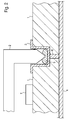
- circuit board 1 shows a sectional view of a section of the device according to the invention is shown.
- the circuit board 1 which may for example consist of several printed circuit board layers, each circuit board layer may have electrical connections.
- electrical components 7 are applied, of which, for example, a part must be shielded so that no electromagnetic interference acts on these components or these components emit no electromagnetic interference to their environment.
- an electrically conductive, usually trough-shaped shield cover 2 is provided, which consists of a base plate having at its edges wall-like, usually perpendicular angled continuations to the electrical components 7, which are to be shielded to enclose.
- the shielding cover 2 shown in Figure 1 is shown here only partially. Usually the shielding covers soldered or glued on the surface of the circuit board 1.
- the shielding cover 2 now has a not completely planar marginal edge or the printed circuit board 1 has a bending or waviness, then it may happen that the shielding cover 2 does not completely rest on the printed circuit board 1 all round, but residual openings remain, due to the interference radiation coming in or out can.
- the circuit board 1 in the area of a recess in which the shield is connected to the circuit board. This recess was lined with a copper layer 3, so that any incoming or outgoing interference between this copper layer 3 and the edge of the shielding cover 2 can only fall in or out meandering, whereby a high shielding effect of this device is achieved.
- the printed circuit board 1 on the side facing away from the shielding cover 2 with a flat copper layer 4, so that interfering radiation which can enter or leave through the printed circuit board 1 is shielded by the sheet-like copper layer 4.
- an adhesive 5 can be used which is electrically conductive and thus the gap between the copper layer 3 of the recess and the edge of the shield 2 is closed by means of an electromagnetically absorbing agent.
- the trench-shaped compound In the case that the printed circuit board 1 is bent or has a ripple or that the edge of the trough-shaped shielding cover 2, which is connected to the circuit board 1, is not sufficiently flat, the trench-shaped compound, this unevenness or waviness can be compensated and a shielding effect of electrical components 7 are achieved, which has no leaks for electromagnetic interference.
- FIG. 2 shows a further embodiment of the invention is shown, in which again the circuit board 1 is shown, which consists for example of several Leiteplatten Anlagenen and electrical components 7 carries. Furthermore, again the trough-shaped shielding cover 2 is shown shielding the electrical components 7 to be shielded from incident interference radiation or preventing interference radiation generated by these components from further propagation.
- a depression is provided in the region of the shielding cover edge which has been provided with a copper layer 3. In the FIG. 2 does not extend over the entire thickness of the printed circuit board in contrast to the recess in FIG.
- connecting holes 6 are provided between the bottom of the recess and the sheet-like copper layer 4 on the side facing away from the shield cover 2, which are often also referred to as vias. These may be drilled, for example, by means of vias or bores between the bottom of the trench-shaped recess and the opposite side and then filled with copper or another conductive material. This results in an electrically conductive connection between the sheet copper layer 4 and the copper layer 3, which lines the trench-shaped depression.
- an adhesive 5 is again provided, which is introduced into the trench-shaped recess and the circuit board 1 and the shield cover 2 firmly connects.
- the connecting holes 6, which are filled with electrically conductive material, as well as the copper layer 3 in the trench-shaped depression and the adhesive 5 forms the electrically conductive shielding cover 2 with the sheet-like copper layer 4 acting in all directions shielding for electromagnetic radiation, so that the electrical components 7 are shielded within this device similar to a Faraday cage. This further ensures that the shield cover 2 and the opposite sheet-like copper layer 4 have a common potential.
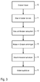
- FIG. 3 shows a production method for producing the device according to the invention.
- this trench-like depression has the shape that the edge of the shielding cover 2 has, so that this edge of the shielding cover 2 can be partially lowered into the depression.
- This trench-like depression is in this case advantageously rectangular executable, so that a frame-shaped depression trench is formed, in which the usually rectangular shielding cover 2 can be fitted.
- communication holes 6 are drilled connecting the bottom of the trench-shaped recess with the opposite side of the printed circuit board.
- both the connecting holes 6 and the depression are coppered, so that the connecting holes 6 are filled with electrically conductive material and the trench-shaped Recess has a copper layer 3.
- adhesive 5 is introduced into the frame-shaped, advantageously rectangular, trench-like depression, this adhesive advantageously being electrically conductive.
- the shield cover is inserted into the recess and pressed so that it touches the adhesive 5 and fills the gap between the edge of the shield cover 2 and the copper layer 3 of the recess.
Landscapes
- Engineering & Computer Science (AREA)
- Microelectronics & Electronic Packaging (AREA)
- Physics & Mathematics (AREA)
- Electromagnetism (AREA)
- Shielding Devices Or Components To Electric Or Magnetic Fields (AREA)
Applications Claiming Priority (1)
| Application Number | Priority Date | Filing Date | Title |
|---|---|---|---|
| DE200410052187 DE102004052187A1 (de) | 2004-10-27 | 2004-10-27 | Vorrichtung zur Abschirmung elektrischer Schaltungen und Verfahren zu deren Herstellung |
Publications (1)
| Publication Number | Publication Date |
|---|---|
| EP1653792A1 true EP1653792A1 (fr) | 2006-05-03 |
Family
ID=35207350
Family Applications (1)
| Application Number | Title | Priority Date | Filing Date |
|---|---|---|---|
| EP05108243A Withdrawn EP1653792A1 (fr) | 2004-10-27 | 2005-09-08 | Dispositif de blindage des circuits électriques et methode pour les produire |
Country Status (2)
| Country | Link |
|---|---|
| EP (1) | EP1653792A1 (fr) |
| DE (1) | DE102004052187A1 (fr) |
Citations (4)
| Publication number | Priority date | Publication date | Assignee | Title |
|---|---|---|---|---|
| JPS5574141A (en) * | 1978-11-27 | 1980-06-04 | Mitsubishi Electric Corp | Plasma etching apparatus |
| JPH1022679A (ja) * | 1996-07-05 | 1998-01-23 | Saitama Nippon Denki Kk | 多層プリント基板のシールド構造 |
| DE10205748A1 (de) | 2002-02-12 | 2003-08-21 | Bosch Gmbh Robert | Vorrichtung und Verfahren zum Frequenzabgleich einer Hochfrequenzschaltung |
| EP1445999A1 (fr) * | 2003-02-07 | 2004-08-11 | Sony Ericsson Mobile Communications AB | Procédé pour munir un circuit imprimé d'un boítier de blindage et le circuit imprimé pour ce |
-
2004
- 2004-10-27 DE DE200410052187 patent/DE102004052187A1/de not_active Withdrawn
-
2005
- 2005-09-08 EP EP05108243A patent/EP1653792A1/fr not_active Withdrawn
Patent Citations (4)
| Publication number | Priority date | Publication date | Assignee | Title |
|---|---|---|---|---|
| JPS5574141A (en) * | 1978-11-27 | 1980-06-04 | Mitsubishi Electric Corp | Plasma etching apparatus |
| JPH1022679A (ja) * | 1996-07-05 | 1998-01-23 | Saitama Nippon Denki Kk | 多層プリント基板のシールド構造 |
| DE10205748A1 (de) | 2002-02-12 | 2003-08-21 | Bosch Gmbh Robert | Vorrichtung und Verfahren zum Frequenzabgleich einer Hochfrequenzschaltung |
| EP1445999A1 (fr) * | 2003-02-07 | 2004-08-11 | Sony Ericsson Mobile Communications AB | Procédé pour munir un circuit imprimé d'un boítier de blindage et le circuit imprimé pour ce |
Non-Patent Citations (2)
| Title |
|---|
| PATENT ABSTRACTS OF JAPAN vol. 004, no. 117 (E - 022) 20 August 1980 (1980-08-20) * |
| PATENT ABSTRACTS OF JAPAN vol. 1998, no. 05 30 April 1998 (1998-04-30) * |
Also Published As
| Publication number | Publication date |
|---|---|
| DE102004052187A1 (de) | 2006-05-04 |
Similar Documents
| Publication | Publication Date | Title |
|---|---|---|
| DE29514398U1 (de) | Abschirmung für Flachbaugruppen | |
| DE102007057533A1 (de) | Kühlkörper und Verfahren zur Herstellung eines Kühlkörpers | |
| DE102014205385A1 (de) | Elektronikmodul, insbesondere für Getriebesteuergerät, mit zwei übereinander gestapelten Leiterplattenelementen | |
| DE69000153T2 (de) | Tragbare, mit bausteinen verbindbare elektronik. | |
| WO2005089033A1 (fr) | Dispositif de commande | |
| EP1365640A2 (fr) | Bo tier et blindage électromagnétiques pour composants électroniques | |
| DE102016224653A1 (de) | Leiterplattenverbund und Verfahren zu dessen Herstellung | |
| DE102017200443A1 (de) | Elektrische Steckkupplungsvorrichtung | |
| DE19518522A1 (de) | Steuergerät für ein Kraftfahrzeug | |
| DE102015208413A1 (de) | Elektrische Verbindungsanordnung | |
| DE102006003137A1 (de) | Elektronikpackung und Packungsverfahren | |
| DE102009027530A1 (de) | Leiterplatte | |
| DE202014006215U1 (de) | Leiterplatte mit gekühltem Baustein, insbesondere SMD-Baustein | |
| DE102008039921B4 (de) | Verfahren zur Herstellung eines elektronischen Geräts mit diskretem Bauelement | |
| DE102016010066B3 (de) | Abschirmungssystem mit an einem Substrat ausgebildetem Stützelement und Verfahren zum Herstellen des Systems | |
| DE102014221973A1 (de) | Elektrisches Gerät für den Einsatz in einem kontaminierenden Medium und Verfahren zur Herstellung eines solchen | |
| DE102010041121A1 (de) | Schaltungsträger sowie Verfahren zur Herstellung eines Schaltungsträgers | |
| DE102015204905A1 (de) | Elektronische Steuervorrichtung | |
| EP1653792A1 (fr) | Dispositif de blindage des circuits électriques et methode pour les produire | |
| DE102007039618A1 (de) | Modul für eine integrierte Steuerelektronik mit vereinfachtem Aufbau | |
| DE102014217186A1 (de) | Verfahren zum Herstellen eines Schaltungsträgers und Schaltungsträger für elektronische Bauelemente | |
| DE112018001014B4 (de) | Elektronische steuervorrichtung | |
| DE102020213582A1 (de) | Hochfrequenzschaltung mit einer Platine und einer Hohlleiterstruktur | |
| DE102020100742A1 (de) | Leiterplatte, Lichtmodul, Beleuchtungseinrichtung und Kraftfahrzeug | |
| DE102018217607A1 (de) | Halbleiterbauelement-Anordnung, Verfahren zu deren Herstellung sowie Entwärmungseinrichtung |
Legal Events
| Date | Code | Title | Description |
|---|---|---|---|
| PUAI | Public reference made under article 153(3) epc to a published international application that has entered the european phase |
Free format text: ORIGINAL CODE: 0009012 |
|
| AK | Designated contracting states |
Kind code of ref document: A1 Designated state(s): AT BE BG CH CY CZ DE DK EE ES FI FR GB GR HU IE IS IT LI LT LU LV MC NL PL PT RO SE SI SK TR |
|
| AX | Request for extension of the european patent |
Extension state: AL BA HR MK YU |
|
| 17P | Request for examination filed |
Effective date: 20061103 |
|
| 17Q | First examination report despatched |
Effective date: 20061211 |
|
| AKX | Designation fees paid |
Designated state(s): DE FR GB IT |
|
| STAA | Information on the status of an ep patent application or granted ep patent |
Free format text: STATUS: THE APPLICATION IS DEEMED TO BE WITHDRAWN |
|
| 18D | Application deemed to be withdrawn |
Effective date: 20070424 |