EP1654592B1 - Messung des flare-effekts auf die linienbreite - Google Patents
Messung des flare-effekts auf die linienbreite Download PDFInfo
- Publication number
- EP1654592B1 EP1654592B1 EP04744097A EP04744097A EP1654592B1 EP 1654592 B1 EP1654592 B1 EP 1654592B1 EP 04744097 A EP04744097 A EP 04744097A EP 04744097 A EP04744097 A EP 04744097A EP 1654592 B1 EP1654592 B1 EP 1654592B1
- Authority
- EP
- European Patent Office
- Prior art keywords
- mask
- box
- flare
- pattern
- features
- Prior art date
- Legal status (The legal status is an assumption and is not a legal conclusion. Google has not performed a legal analysis and makes no representation as to the accuracy of the status listed.)
- Expired - Lifetime
Links
- 230000000694 effects Effects 0.000 title claims abstract description 24
- 238000000034 method Methods 0.000 claims abstract description 37
- 238000005259 measurement Methods 0.000 claims abstract description 25
- 239000000758 substrate Substances 0.000 claims abstract description 23
- 238000004904 shortening Methods 0.000 claims abstract description 12
- 239000002131 composite material Substances 0.000 claims abstract description 10
- 229920002120 photoresistant polymer Polymers 0.000 claims abstract description 7
- 238000000206 photolithography Methods 0.000 claims abstract description 6
- 238000012937 correction Methods 0.000 claims description 15
- 235000012431 wafers Nutrition 0.000 description 16
- 238000004519 manufacturing process Methods 0.000 description 14
- 239000004065 semiconductor Substances 0.000 description 13
- 230000003287 optical effect Effects 0.000 description 5
- XUIMIQQOPSSXEZ-UHFFFAOYSA-N Silicon Chemical compound [Si] XUIMIQQOPSSXEZ-UHFFFAOYSA-N 0.000 description 3
- 230000004075 alteration Effects 0.000 description 3
- 238000005530 etching Methods 0.000 description 3
- 230000000873 masking effect Effects 0.000 description 3
- 239000000463 material Substances 0.000 description 3
- 238000012545 processing Methods 0.000 description 3
- 229910052710 silicon Inorganic materials 0.000 description 3
- 239000010703 silicon Substances 0.000 description 3
- 238000004364 calculation method Methods 0.000 description 2
- 238000005516 engineering process Methods 0.000 description 2
- 238000012544 monitoring process Methods 0.000 description 2
- VYZAMTAEIAYCRO-UHFFFAOYSA-N Chromium Chemical compound [Cr] VYZAMTAEIAYCRO-UHFFFAOYSA-N 0.000 description 1
- 238000013459 approach Methods 0.000 description 1
- 230000015572 biosynthetic process Effects 0.000 description 1
- 230000000295 complement effect Effects 0.000 description 1
- 238000005286 illumination Methods 0.000 description 1
- 239000007788 liquid Substances 0.000 description 1
- 238000001459 lithography Methods 0.000 description 1
- 238000004377 microelectronic Methods 0.000 description 1
- 238000009877 rendering Methods 0.000 description 1
- 230000000717 retained effect Effects 0.000 description 1
- 239000007787 solid Substances 0.000 description 1
- 239000000126 substance Substances 0.000 description 1
- 238000012795 verification Methods 0.000 description 1
Images




Classifications
-
- G—PHYSICS
- G03—PHOTOGRAPHY; CINEMATOGRAPHY; ANALOGOUS TECHNIQUES USING WAVES OTHER THAN OPTICAL WAVES; ELECTROGRAPHY; HOLOGRAPHY
- G03F—PHOTOMECHANICAL PRODUCTION OF TEXTURED OR PATTERNED SURFACES, e.g. FOR PRINTING, FOR PROCESSING OF SEMICONDUCTOR DEVICES; MATERIALS THEREFOR; ORIGINALS THEREFOR; APPARATUS SPECIALLY ADAPTED THEREFOR
- G03F1/00—Originals for photomechanical production of textured or patterned surfaces, e.g., masks, photo-masks, reticles; Mask blanks or pellicles therefor; Containers specially adapted therefor; Preparation thereof
- G03F1/62—Pellicles, e.g. pellicle assemblies, e.g. having membrane on support frame; Preparation thereof
-
- G—PHYSICS
- G03—PHOTOGRAPHY; CINEMATOGRAPHY; ANALOGOUS TECHNIQUES USING WAVES OTHER THAN OPTICAL WAVES; ELECTROGRAPHY; HOLOGRAPHY
- G03F—PHOTOMECHANICAL PRODUCTION OF TEXTURED OR PATTERNED SURFACES, e.g. FOR PRINTING, FOR PROCESSING OF SEMICONDUCTOR DEVICES; MATERIALS THEREFOR; ORIGINALS THEREFOR; APPARATUS SPECIALLY ADAPTED THEREFOR
- G03F1/00—Originals for photomechanical production of textured or patterned surfaces, e.g., masks, photo-masks, reticles; Mask blanks or pellicles therefor; Containers specially adapted therefor; Preparation thereof
- G03F1/36—Masks having proximity correction features; Preparation thereof, e.g. optical proximity correction [OPC] design processes
-
- G—PHYSICS
- G03—PHOTOGRAPHY; CINEMATOGRAPHY; ANALOGOUS TECHNIQUES USING WAVES OTHER THAN OPTICAL WAVES; ELECTROGRAPHY; HOLOGRAPHY
- G03F—PHOTOMECHANICAL PRODUCTION OF TEXTURED OR PATTERNED SURFACES, e.g. FOR PRINTING, FOR PROCESSING OF SEMICONDUCTOR DEVICES; MATERIALS THEREFOR; ORIGINALS THEREFOR; APPARATUS SPECIALLY ADAPTED THEREFOR
- G03F1/00—Originals for photomechanical production of textured or patterned surfaces, e.g., masks, photo-masks, reticles; Mask blanks or pellicles therefor; Containers specially adapted therefor; Preparation thereof
- G03F1/38—Masks having auxiliary features, e.g. special coatings or marks for alignment or testing; Preparation thereof
- G03F1/44—Testing or measuring features, e.g. grid patterns, focus monitors, sawtooth scales or notched scales
-
- G—PHYSICS
- G03—PHOTOGRAPHY; CINEMATOGRAPHY; ANALOGOUS TECHNIQUES USING WAVES OTHER THAN OPTICAL WAVES; ELECTROGRAPHY; HOLOGRAPHY
- G03F—PHOTOMECHANICAL PRODUCTION OF TEXTURED OR PATTERNED SURFACES, e.g. FOR PRINTING, FOR PROCESSING OF SEMICONDUCTOR DEVICES; MATERIALS THEREFOR; ORIGINALS THEREFOR; APPARATUS SPECIALLY ADAPTED THEREFOR
- G03F1/00—Originals for photomechanical production of textured or patterned surfaces, e.g., masks, photo-masks, reticles; Mask blanks or pellicles therefor; Containers specially adapted therefor; Preparation thereof
- G03F1/68—Preparation processes not covered by groups G03F1/20 - G03F1/50
- G03F1/70—Adapting basic layout or design of masks to lithographic process requirements, e.g., second iteration correction of mask patterns for imaging
-
- G—PHYSICS
- G03—PHOTOGRAPHY; CINEMATOGRAPHY; ANALOGOUS TECHNIQUES USING WAVES OTHER THAN OPTICAL WAVES; ELECTROGRAPHY; HOLOGRAPHY
- G03F—PHOTOMECHANICAL PRODUCTION OF TEXTURED OR PATTERNED SURFACES, e.g. FOR PRINTING, FOR PROCESSING OF SEMICONDUCTOR DEVICES; MATERIALS THEREFOR; ORIGINALS THEREFOR; APPARATUS SPECIALLY ADAPTED THEREFOR
- G03F7/00—Photomechanical, e.g. photolithographic, production of textured or patterned surfaces, e.g. printing surfaces; Materials therefor, e.g. comprising photoresists; Apparatus specially adapted therefor
- G03F7/70—Microphotolithographic exposure; Apparatus therefor
- G03F7/70483—Information management; Active and passive control; Testing; Wafer monitoring, e.g. pattern monitoring
- G03F7/70591—Testing optical components
-
- G—PHYSICS
- G03—PHOTOGRAPHY; CINEMATOGRAPHY; ANALOGOUS TECHNIQUES USING WAVES OTHER THAN OPTICAL WAVES; ELECTROGRAPHY; HOLOGRAPHY
- G03F—PHOTOMECHANICAL PRODUCTION OF TEXTURED OR PATTERNED SURFACES, e.g. FOR PRINTING, FOR PROCESSING OF SEMICONDUCTOR DEVICES; MATERIALS THEREFOR; ORIGINALS THEREFOR; APPARATUS SPECIALLY ADAPTED THEREFOR
- G03F7/00—Photomechanical, e.g. photolithographic, production of textured or patterned surfaces, e.g. printing surfaces; Materials therefor, e.g. comprising photoresists; Apparatus specially adapted therefor
- G03F7/70—Microphotolithographic exposure; Apparatus therefor
- G03F7/70483—Information management; Active and passive control; Testing; Wafer monitoring, e.g. pattern monitoring
- G03F7/70605—Workpiece metrology
- G03F7/70616—Monitoring the printed patterns
-
- G—PHYSICS
- G03—PHOTOGRAPHY; CINEMATOGRAPHY; ANALOGOUS TECHNIQUES USING WAVES OTHER THAN OPTICAL WAVES; ELECTROGRAPHY; HOLOGRAPHY
- G03F—PHOTOMECHANICAL PRODUCTION OF TEXTURED OR PATTERNED SURFACES, e.g. FOR PRINTING, FOR PROCESSING OF SEMICONDUCTOR DEVICES; MATERIALS THEREFOR; ORIGINALS THEREFOR; APPARATUS SPECIALLY ADAPTED THEREFOR
- G03F7/00—Photomechanical, e.g. photolithographic, production of textured or patterned surfaces, e.g. printing surfaces; Materials therefor, e.g. comprising photoresists; Apparatus specially adapted therefor
- G03F7/70—Microphotolithographic exposure; Apparatus therefor
- G03F7/708—Construction of apparatus, e.g. environment aspects, hygiene aspects or materials
- G03F7/70908—Hygiene, e.g. preventing apparatus pollution, mitigating effect of pollution or removing pollutants from apparatus
- G03F7/70941—Stray fields and charges, e.g. stray light, scattered light, flare, transmission loss
Definitions
- the invention relates to semiconductor process. More particularly the invention relates to measuring the degree of flare distortion of printed features.
- MOS metal-oxide-semiconductor
- PMOS p-channel MOS
- NMOS n-channel MOS
- CMOS complementary MOS
- bipolar transistors bipolar transistors
- BiCMOS transistors bipolar transistors
- Each of these semiconductor devices generally includes a semiconductor substrate on which a number of active devices are formed.
- the particular structure of a given active device can vary between device types.
- an active device generally includes source and drain regions and a gate electrode that modulates current between the source and drain regions.
- etching One important step in the manufacturing of such devices is the formation of devices, or portions thereof, using photolithography and etching processes.
- photolithography a wafer substrate is coated with a light-sensitive material called photo-resist.
- the wafer is exposed to light; the light striking the wafer is passed through a mask plate.
- This mask plate defines the desired features to be printed on the substrate.
- the resist-coated wafer substrate is developed.
- the desired features as defined on the mask are retained on the photo resist-coated substrate.
- Unexposed areas of resist are washed away with a developer.
- the wafer having the desired features defined is subjected to etching.
- the etching may either be a wet etch, in which liquid chemicals are used to remove wafer material or a dry etch, in which wafer material is subjected to a radio frequency (RF) induced plasma.
- RF radio frequency
- CDs critical dimensions
- wafer fabrication becomes more reliant on maintaining consistent CDs over normal process variations.
- the active device dimensions as designed and replicated on the photo mask and those actually rendered on the wafer substrate have to be repeatable and controllable.
- the process attempts to maintain the final CDs equal to the masking CDs.
- imperfections in the process or changes in technology that may be realized in a given fabrication process, if the process were "tweaked" often necessitate the rendering of final CDs that deviate from the masking CDs.
- U.S. Patent 5,757,507 of Austent et al. relates generally to manufacturing processes requiring lithography and, more particularly, to monitoring of bias and overlay error in lithographic and etch processes used in microelectronics manufacturing which is particularly useful more monitoring pattern features with dimensions on the order of less than 0.5 micron.
- U.S. Patent 5,962,173 of Leroux et al. relates generally to the field of fabricating integrated circuits and more particularly to maintaining accuracy in the fabrication of such circuits having extremely narrow line elements such as gate lines.
- U.S. Patent 5,902, 703 of Leroux et al. relates generally to the field of fabricating integrated circuits and more particularly to maintaining accuracy in the fabrication of such circuits having relatively narrow line elements such as gate lines.
- the invention is also directed to the verification of stepper lens fabrication quality.
- U.S. Patent 5,976,741 of Ziger et al. relates generally to methods of determining illumination exposure dosages and other processing parameters in the field of fabricating integrated circuits. More particularly, the invention concerns methods of processing semiconductor wafers in step and repeat systems.
- U.S. Patent 6,301,008 B1 of Ziger et al. relates to semiconductor devices and their manufacture, and more particularly, to arrangements and processes for developing relatively narrow line widths of elements such as gate lines, while maintaining accuracy in their fabrication.
- U.S. Patent Application US 2002/0182516 A1 of Bowes relates generally to metrology of semiconductor manufacturing processes. More particularly, the present invention is a needle comb reticle pattern for simultaneously making critical dimension (CD) measurements of device features and registration measurements of mask overlays relative to semiconductor wafers during processing of semiconductor wafers.
- CD critical dimension
- Lens aberrations limit the quality of reproducing a mask pattern into a photo resist.
- a significant type of lens aberrations is flare in which stray light can distort printed features. Flare can vary widely from stepper to stepper even from lenses of the same stepper family. In the manufacture of semiconductors, it is important to be able to assess the effect of flare due to various exposure tools. In general, flare degrades resist profiles by exposing regions that otherwise should remain underexposed. There is a need for quantifying the effects of flare so that the user may take action to minimize these effects so that product yield is increased and costs may be lowered.
- US 2003/0068565 discloses a method for use in identifying flare using a two-mask photolithographic process which compares transmittive features in a light shielding layer with transmittive features in an area where the light shielding layer is left only around the transmittive features.
- the document discloses the measurement of line width for determining flare.
- a method for determining the effect of flare on line shortening within a photo lithography process on a photo resist coated substrate comprising:
- the invention also provides a mask set for use in a wafer stepper, the mask set comprising: a first mask having features of predetermined dimensions laid out in a dark-field, the features comprising: a first portion of a flare pattern; a first portion of a box-in- a-box correction pattern; and a first portion of a focus box pattern; a second mask having features of predetermined dimensions laid out in a light-field, the features comprising: a second portion of the flare pattern; a second portion of the box-in- a-box correction pattern; the second portion of the box-in-a-box correction pattern alignable to the first portion of the box-in-a-box correction pattern; and a second portion of the focus box pattern, the second portion of the focus box pattern alignable to the first portion of the focus box pattern.
- the present invention has been found to be useful for quantifying the effects of flare in reproducing a mask pattern onto a photo resist coated substrate.
- a modified box-in-a-box structure 100 is constructed using two masks, a sparse (clear-field) mask that is sensitive to flare and a dense (dark-field) mask that is far less sensitive to flare.
- the sides of the box-in-a-box are composed of grating structures.
- the left and bottom elements 110 are exposed using a dark-field mask.
- the top and right elements 120 are exposed from a clear-field mask.
- the user may assume that the masking can be done such that there is negligible overlay error for exposing two masks to attain the elements 110 and 120.
- the apparent misalignment is a relative measure of the effect of flare line length shortening. It is expected that the elements 120 exposed with the clear-field mask are somewhat shorter than those elements 110 exposed with the dark-field mask.
- df x is the field optical length measurement of the part of the box structure exposed with the dark field mask
- 1f x is the corresponding optical length measurement of the part of the box exposed with the light field mask.
- the corresponding optical length measurements in the y-direction are df y and 1f y .
- the dark-field mask 200 is composed of grating structures 210 and an alignment box 230.
- the clear-field mask 205 is composed of grating structure 220 and another alignment box 240. In using these masks on a photo resist coated substrate, the user may print the dark-field pattern of FIG. 2A .
- the clear-field pattern of FIG. 2B is aligned to the print of FIG. 2A with the two alignment boxes 230 and 240.
- the resulting pattern 215 of FIG. 2C produces the flare pattern of grating structures 210 and 220 and a box-in-a-box alignment patter 250 (boxes 230 and 240).
- the measurement of interest is the width of each side. Differences in the left and right or top and bottom are the sum of the misalignment between the two masks and any flare differences. We can subtract the effect of mask overlay with the standard box-in-box.
- a second potential error that may be encountered is due to long range flare effects in which scattered light exposes those areas masked off.
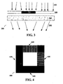
- FIG. 3 In the arrangement 300, light 310 is projection through a mask 320 having a defined designed feature 330. Aberrations in lens 340 scatter the light 310b. This scattering may cause the printed features to be larger than those designed. In an extreme, example, the scattered light would evenly expose areas under the masked regions. One of the assumptions being made is that regions under the chrome are not exposed. The effect of long-range flare is worse with the light field mask.
- FIG. 5 For example, the procedure is to expose Fig. 5A and then Fig. 5B . We assume that the left and bottom regions which are masked off area (the thick "L" of the 515 structure), remain completely unexposed.
- a correction scheme according to an embodiment of the present invention may be used to quantify this error.
- FIG. 4 1 One or more stepper fields are exposed with a focus box pattern 400 using a dark-field mask.
- the focus box pattern 400 is composed of solid regions 410, 420 and lines and spaces 430, 440 in the x and y-direction. 2).
- the same pattern is exposed in a region that has been masked off in a prior clear-field exposure. 3).
- the correction for prior exposure due to flare is the difference in line shortening between the focus box structure in the single exposed field and the doubly exposed field.
- the focus box pattern of FIG. 4 may be incorporated into the flare measurement structure of FIGS. 2A - 2C .
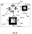
- a dark-field mask 500 is composed of part of a flare pattern 510, an alignment box 520 and a focus box pattern 530.
- a corresponding clear-field mask 505 is composed of another alignment box 525 (which aligns to alignment box 520), the region defined by focus box pattern 530 is blocked out by region 535.
- the printed composite structure, FIG. 5C is the combination of dark field mask 500 and clear-field mask 505. Patterns 510 and 515 make the flare pattern ("A").
- the correction box ("B") 535, and focus box (“C”) pattern 530 are the combination of the dark field mask 500 and light-field mask 505.
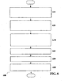
- the user may print the dark-field mask pattern 610 of FIG. 5A . Overlaid upon the exposed FIG. 5A pattern, the user may print the clear-field mask pattern 620 of FIG. 5B .
- the resist coated-coated substrate has undergone a double-exposure for the FIG. 5A and FIG. 5B masks. Having printed FIG. 5A and FIG. 5B mask patterns as a double-exposure, the user steps to another location on the substrate and prints the composite mask pattern 630 of FIG. 5C .
- the printed pattern is developed 640. The user obtains measurements from the printed pattern 650. After obtaining the measurements, the user may determine the effect of flare 660 on line shortening.
- the user may print the combination mask pattern of FIG. 5A and 5B , as depicted in FIG. 5C in a single exposure.
- the user prints the combination pattern 710 which includes the flare pattern (510, 515), correction box (535), and focus box (530).
- the printed pattern is developed 720.
- the effect of long-range flare on line shortening 730 is determined.
- R the measured registration reported by the alignment-measuring patterns, as depicted in FIG. 5C .
- R x right leg - left leg / 2
- R y top leg - bottom leg / 2
- the user may determine the degree of misalignment in the "B" structure 535 between the overlay FIG. 5A and FIG. 5B in the x-direction where the misalignment is the difference in width between the structure's left leg (cb1 x ) and right leg (cb2 x ) and in the y-direction where the misalignment is the difference between the bottom leg (cb1 y ) and the top leg (cb2 y ).
- the user may determine the degree of misalignment in the "A" structure between the light-field features 515and dark-field features 510.
- the apparent misalignment in the x-direction, between the light/dark field features is the difference in width between the structure's left leg (df x ) and right leg (1f x ) and the apparent misalignment in the y-direction between the light/dark field features is the difference in width between the structure's top leg (1f y ) and bottom leg (dfy).
- the user may compare the line shortening between the "C" structure 530 in the single versus double exposed fields where line shortening in the x-direction, is the difference in width between the left leg (fb1 x ) and right leg (fb2 x ) or in the y-direction, the top leg (fb2 y ) and bottom leg (fb1 y ).
- the intermediate results of the calculations determined from the three structures is used to calculate the flare.
- r x 1f-df , r x 1st-2nd mask and r x Multiple-single Exposure are the measured misalignments in the x direction for the light field/dark field structures (A), the standard box in box (B) that measures the alignment between the two exposures and the measured difference between the focus box structure (C) exposed twice versus a single time.
- the alignment tool reports r x and r y which are the differences in left leg and right leg or top leg and bottom leg optical width measurements.
- r x and r y are the differences in left leg and right leg or top leg and bottom leg optical width measurements.
Landscapes
- General Physics & Mathematics (AREA)
- Physics & Mathematics (AREA)
- Health & Medical Sciences (AREA)
- Epidemiology (AREA)
- Public Health (AREA)
- Environmental & Geological Engineering (AREA)
- Engineering & Computer Science (AREA)
- Atmospheric Sciences (AREA)
- Life Sciences & Earth Sciences (AREA)
- Exposure And Positioning Against Photoresist Photosensitive Materials (AREA)
- Exposure Of Semiconductors, Excluding Electron Or Ion Beam Exposure (AREA)
- Semiconductor Lasers (AREA)
- Apparatus For Radiation Diagnosis (AREA)
Claims (11)
- Verfahren zum Bestimmen der Auswirkung von Lichtreflexen auf die Linienverkürzung innerhalb eines Photolithographieprozesses (600) auf einem photoresistbeschichteten Substrat, wobei das Verfahren umfasst:Drucken einer ersten Maske (200), die ein Lichtreflexmuster entsprechend einer Ecke der ersten Maske aufweist, an einer ersten Rohchip-Position auf dem Substrat und bei einer ersten Belichtung, und Drucken einer zweiten Maske (205), die ein weiteres Lichtreflexmuster entsprechend einer gegenüberliegenden Ecke der zweiten Maske aufweist, bei einer zweiten Belichtung;Drucken eines zusammengesetzten Maskenmusters (215), das auf Merkmalen der ersten Maske und der zweiten Maske beruht, an einer zweiten Rohchip-Position auf dem Substrat;Entwickeln der gedruckten Muster (640) und Erlangen von Messungen (650) hiervon; undBestimmen der Auswirkung von Lichtreflexen (660) als Funktion der Messungen.
- Verfahren nach Anspruch 1, wobei das Erlangen der Messungen ferner umfasst:Messen des Lichtreflexmusters, dass der einen Ecke der ersten Maske zugeordnet ist; undMessen des Lichtreflexmusters, dass der gegenüberliegenden Ecke der zweiten Maske zugeordnet ist.
- Verfahren nach Anspruch 2, wobei das Erlangen der Messungen ferner umfasst:Messen des zusammengesetzten Maskenmusters an Stellen, die durch Merkmale der ersten Maske und Merkmale der zweiten Maske definiert sind.
- Verfahren nach Anspruch 1, wobei:die erste Maske eine Dunkelfeldmaske (200) ist, die ferner eine Korrekturfachöffnung und ein Fokusfachmuster auf dem Substrat umfasst; unddie zweite Maske eine Klarfeldmaske (205) ist.
- Verfahren nach Anspruch 4, wobei das Erlangen der Messungen ferner umfasst:Messen der Abmessungen des Lichtreflexfachmusters (510, 515) der mit der Dunkelfeldmaske gedruckten Merkmale und der mit der Klarfeldmaske gedruckten Merkmale;Messen der Abmessungen der Korrekturfachmerkmale (535), die während der ersten Belichtung gedruckt worden sind, und der Merkmale, die während der zweiten Belichtung gedruckt worden sind; undMessen der Abmessungen des Fokusfachmusters (530), das während des Stepping zur ersten Rohchip-Position gedruckt worden ist, und Messen der Abmessungen des Fokusfachmusters, das an der zweiten Rohchip-Position gedruckt worden ist.
- Verfahren nach Anspruch 5, wobei das Erlangen der Messungen das Aufnehmen von Messungen von einem linken Schenkel und von einem rechten Schenkel der gedruckten Merkmale, sowie das Aufnehmen von Messungen von einem oberen Schenkel und von einem unteren Schenkel der gedruckten Merkmale umfasst.
- Verfahren nach Anspruch 5, wobei die Auswirkung von Lichtreflexen eine Funktion der Differenzen zwischen dem linken Schenkel und dem rechten Schenkel eines gegebenen gedruckten Merkmals für die X-Richtung ist; und wobei die Auswirkung von Lichtreflexen eine Funktion der Differenzen zwischen dem oberen Schenkel und dem unteren Schenkel eines gegebenen gedruckten Merkmals für die Y-Richtung ist.
- Verfahren nach Anspruch 7, wobei die Auswirkung von Lichtreflexen durch die folgende Gleichung definiert ist:

wobei rn 1f-df, rn 1-2. Maske, rn mehrfache-einfache Belichtung die gemessenen Fehlausrichtungen in einer gegebenen Richtung n für die Lichtfeld/Dunkelfeld-Strukturen (A), das Standardfach im Fach (B), das die Ausrichtung zwischen den zwei Belichtungen misst, und die gemessene Differenz zwischen der Fokusfachstruktur (C) bei doppelter gegenüber einfacher Belichtung sind. - Verfahren nach Anspruch 8, wobei n die X-Richtung und die Y-Richtung umfasst.
- Maskensatz (500, 505) zur Verwendung in einem Waver-Stepper, wobei der Maskensatz umfasst:eine erste Maske (500), die Merkmale mit vorgegebenen Abmessungen aufweist, die in einem Dunkelfeld angeordnet sind, wobei die Merkmale umfassen: einen ersten Abschnitt (510) eines Lichtreflexmusters; einen ersten Abschnitt (520) eines Fach-in-Fach-Korrekturmusters; und einen ersten Abschnitt (530) eines Fokusfachmusters;eine zweite Maske (505) die Merkmale mit vorgegebenen Abmessungen aufweist, die in einem Lichtfeld angeordnet sind, wobei die Merkmale umfassen: einen zweiten Abschnitt (515) des Lichtreflexmusters; einen zweiten Abschnitt (520) des Fach-in-Fach-Korrekturmusters, wobei der zweite Abschnitt des Fach-in-Fach-Korrekturmusters auf den ersten Abschnitt des Fach-in-Fach-Korrekturmusters ausrichtbar ist; und einen zweiten Abschnitt (535) des Fokusfachmusters, wobei der zweite Abschnitt des Fokusfachmusters auf den ersten Abschnitt des Fokusfachmusters ausrichtbar ist.
- Maskensatz nach Anspruch 10, der ferner eine dritte Maske (555) umfasst, die Merkmale mit vorgegebenen Abmessungen aufweist, wobei die Merkmale durch die Kombination der Merkmale der ersten Maske (500) und der Merkmale der zweiten Maske (505) definiert sind.
Applications Claiming Priority (2)
| Application Number | Priority Date | Filing Date | Title |
|---|---|---|---|
| US49213003P | 2003-08-01 | 2003-08-01 | |
| PCT/IB2004/002444 WO2005013004A2 (en) | 2003-08-01 | 2004-07-31 | Measuring the effect of flare on line width |
Publications (2)
| Publication Number | Publication Date |
|---|---|
| EP1654592A2 EP1654592A2 (de) | 2006-05-10 |
| EP1654592B1 true EP1654592B1 (de) | 2008-10-01 |
Family
ID=34115601
Family Applications (1)
| Application Number | Title | Priority Date | Filing Date |
|---|---|---|---|
| EP04744097A Expired - Lifetime EP1654592B1 (de) | 2003-08-01 | 2004-07-31 | Messung des flare-effekts auf die linienbreite |
Country Status (9)
| Country | Link |
|---|---|
| US (2) | US7556900B2 (de) |
| EP (1) | EP1654592B1 (de) |
| JP (1) | JP2007501508A (de) |
| KR (1) | KR20060056358A (de) |
| CN (1) | CN1833205B (de) |
| AT (1) | ATE409892T1 (de) |
| DE (1) | DE602004016860D1 (de) |
| TW (1) | TW200518185A (de) |
| WO (1) | WO2005013004A2 (de) |
Families Citing this family (7)
| Publication number | Priority date | Publication date | Assignee | Title |
|---|---|---|---|---|
| TWI431663B (zh) * | 2004-09-30 | 2014-03-21 | 尼康股份有限公司 | Measurement method and exposure method, and component manufacturing method |
| JP2008535223A (ja) * | 2005-03-23 | 2008-08-28 | アギア システムズ インコーポレーテッド | インプリント・リソグラフィおよび直接描画技術を用いるデバイス製造方法 |
| JP4882371B2 (ja) | 2005-12-27 | 2012-02-22 | 富士通セミコンダクター株式会社 | フレア量の計測方法、フレア量計測用マスク及びデバイスの製造方法 |
| JP2008010793A (ja) * | 2006-06-30 | 2008-01-17 | Fujitsu Ltd | 露光位置マークの位置ずれ検出方法 |
| US8105736B2 (en) * | 2008-03-13 | 2012-01-31 | Miradia Inc. | Method and system for overlay correction during photolithography |
| CN102543956B (zh) * | 2010-12-08 | 2016-07-06 | 无锡华润上华科技有限公司 | 多层套刻标记 |
| JP2013062433A (ja) * | 2011-09-14 | 2013-04-04 | Toshiba Corp | パターン生成方法、パターン形成方法およびパターン生成プログラム |
Family Cites Families (10)
| Publication number | Priority date | Publication date | Assignee | Title |
|---|---|---|---|---|
| KR0172558B1 (ko) * | 1995-03-22 | 1999-03-20 | 김주용 | 노광 마스크의 제조방법 |
| US5757507A (en) * | 1995-11-20 | 1998-05-26 | International Business Machines Corporation | Method of measuring bias and edge overlay error for sub-0.5 micron ground rules |
| US6301008B1 (en) * | 1997-03-27 | 2001-10-09 | Philips Semiconductor, Inc. | Arrangement and method for calibrating optical line shortening measurements |
| US5962173A (en) * | 1997-03-27 | 1999-10-05 | Vlsi Technology, Inc. | Method for measuring the effectiveness of optical proximity corrections |
| US5902703A (en) * | 1997-03-27 | 1999-05-11 | Vlsi Technology, Inc. | Method for measuring dimensional anomalies in photolithographed integrated circuits using overlay metrology, and masks therefor |
| US5976741A (en) * | 1997-10-21 | 1999-11-02 | Vsli Technology, Inc. | Methods for determining illumination exposure dosage |
| US6730444B2 (en) * | 2001-06-05 | 2004-05-04 | Micron Technology, Inc. | Needle comb reticle pattern for critical dimension and registration measurements using a registration tool and methods for using same |
| US6835507B2 (en) * | 2001-08-08 | 2004-12-28 | Samsung Electronics Co., Ltd. | Mask for use in measuring flare, method of manufacturing the mask, method of identifying flare-affected region on wafer, and method of designing new mask to correct for flare |
| US7393619B2 (en) * | 2003-05-08 | 2008-07-01 | Yuji Yamaguchi | Method and lithographic structure for measuring lengths of lines and spaces |
| US7332255B2 (en) * | 2004-05-07 | 2008-02-19 | Nxp B.V. | Overlay box structure for measuring process induced line shortening effect |
-
2004
- 2004-07-29 TW TW093122641A patent/TW200518185A/zh unknown
- 2004-07-31 KR KR1020067002259A patent/KR20060056358A/ko not_active Withdrawn
- 2004-07-31 US US10/566,804 patent/US7556900B2/en not_active Expired - Fee Related
- 2004-07-31 WO PCT/IB2004/002444 patent/WO2005013004A2/en not_active Ceased
- 2004-07-31 EP EP04744097A patent/EP1654592B1/de not_active Expired - Lifetime
- 2004-07-31 DE DE602004016860T patent/DE602004016860D1/de not_active Expired - Lifetime
- 2004-07-31 CN CN2004800223945A patent/CN1833205B/zh not_active Expired - Fee Related
- 2004-07-31 AT AT04744097T patent/ATE409892T1/de not_active IP Right Cessation
- 2004-07-31 JP JP2006521700A patent/JP2007501508A/ja not_active Withdrawn
-
2009
- 2009-05-12 US US12/464,731 patent/US7709166B2/en not_active Expired - Fee Related
Also Published As
| Publication number | Publication date |
|---|---|
| CN1833205B (zh) | 2011-02-16 |
| US7556900B2 (en) | 2009-07-07 |
| KR20060056358A (ko) | 2006-05-24 |
| WO2005013004A3 (en) | 2005-07-21 |
| ATE409892T1 (de) | 2008-10-15 |
| WO2005013004A2 (en) | 2005-02-10 |
| US7709166B2 (en) | 2010-05-04 |
| DE602004016860D1 (de) | 2008-11-13 |
| US20060210885A1 (en) | 2006-09-21 |
| US20090220870A1 (en) | 2009-09-03 |
| EP1654592A2 (de) | 2006-05-10 |
| CN1833205A (zh) | 2006-09-13 |
| TW200518185A (en) | 2005-06-01 |
| JP2007501508A (ja) | 2007-01-25 |
Similar Documents
| Publication | Publication Date | Title |
|---|---|---|
| US7244533B2 (en) | Method of the adjustable matching map system in lithography | |
| US20020105649A1 (en) | Method and apparatus for self-referenced wafer stage positional error mapping | |
| US7709166B2 (en) | Measuring the effect of flare on line width | |
| JP2854551B2 (ja) | 露光マスクの製造方法 | |
| JP2001022051A (ja) | レチクル及び半導体装置の製造方法 | |
| KR100549153B1 (ko) | 포토 마스크의 제조 방법 | |
| US6420077B1 (en) | Contact hole model-based optical proximity correction method | |
| US20050117154A1 (en) | Method and apparatus for self-referenced projection lens distortion mapping | |
| KR100472411B1 (ko) | 반도체 장치의 제조방법 및 오버레이 검사마크를 가진반도체 장치 | |
| US6656646B2 (en) | Fabrication method of semiconductor integrated circuit device | |
| US7033903B2 (en) | Method and apparatus for forming patterned photoresist layer | |
| US7262398B2 (en) | Method and apparatus for self-referenced dynamic step and scan intra-field scanning distortion | |
| US6414326B1 (en) | Technique to separate dose-induced vs. focus-induced CD or linewidth variation | |
| US7332255B2 (en) | Overlay box structure for measuring process induced line shortening effect | |
| US7393619B2 (en) | Method and lithographic structure for measuring lengths of lines and spaces | |
| US5928820A (en) | Method for measuring pattern line width during manufacture of a semiconductor device | |
| US6370680B1 (en) | Device to determine line edge roughness effect on device performance | |
| KR20010028305A (ko) | 위치정합 보정 방법 | |
| KR100529428B1 (ko) | 근접 효과 보정용 마스크를 이용한 패턴 형성용 마스크제작 방법 | |
| KR100780761B1 (ko) | 마스크 프로세스를 통한 위치 보정 제어 방법 | |
| KR0122514B1 (ko) | 반도체소자의 노광공정시의 촛점심도 여유도 측정방법 | |
| KR0146244B1 (ko) | 포토 마스크장치 및 포토 마스크 제조 에러 측정방법 | |
| KR20010058325A (ko) | 레지스트레이션 에러 측정용 패턴이 구비된 레티클 및레지스트레이션 에러 측정용 패턴의 형성방법 | |
| KR20040059717A (ko) | 포토마스크의 레지스트레이션을 이용한 반도체 제조 방법 | |
| KR20030000840A (ko) | 반도체 소자의 오버레이 측정 패턴 형성방법 |
Legal Events
| Date | Code | Title | Description |
|---|---|---|---|
| PUAI | Public reference made under article 153(3) epc to a published international application that has entered the european phase |
Free format text: ORIGINAL CODE: 0009012 |
|
| 17P | Request for examination filed |
Effective date: 20060301 |
|
| AK | Designated contracting states |
Kind code of ref document: A2 Designated state(s): AT BE BG CH CY CZ DE DK EE ES FI FR GB GR HU IE IT LI LU MC NL PL PT RO SE SI SK TR |
|
| 17Q | First examination report despatched |
Effective date: 20060629 |
|
| DAX | Request for extension of the european patent (deleted) | ||
| RIN1 | Information on inventor provided before grant (corrected) |
Inventor name: LEROUX, PIERRE,C/O NXP SEMICONDUCTORS-IP DEPT. Inventor name: ZIGER, DAVID |
|
| RAP1 | Party data changed (applicant data changed or rights of an application transferred) |
Owner name: NXP B.V. |
|
| GRAP | Despatch of communication of intention to grant a patent |
Free format text: ORIGINAL CODE: EPIDOSNIGR1 |
|
| GRAS | Grant fee paid |
Free format text: ORIGINAL CODE: EPIDOSNIGR3 |
|
| GRAC | Information related to communication of intention to grant a patent modified |
Free format text: ORIGINAL CODE: EPIDOSCIGR1 |
|
| GRAA | (expected) grant |
Free format text: ORIGINAL CODE: 0009210 |
|
| AK | Designated contracting states |
Kind code of ref document: B1 Designated state(s): AT BE BG CH CY CZ DE DK EE ES FI FR GB GR HU IE IT LI LU MC NL PL PT RO SE SI SK TR |
|
| REG | Reference to a national code |
Ref country code: GB Ref legal event code: FG4D |
|
| REG | Reference to a national code |
Ref country code: CH Ref legal event code: EP |
|
| REG | Reference to a national code |
Ref country code: IE Ref legal event code: FG4D |
|
| REF | Corresponds to: |
Ref document number: 602004016860 Country of ref document: DE Date of ref document: 20081113 Kind code of ref document: P |
|
| PG25 | Lapsed in a contracting state [announced via postgrant information from national office to epo] |
Ref country code: SI Free format text: LAPSE BECAUSE OF FAILURE TO SUBMIT A TRANSLATION OF THE DESCRIPTION OR TO PAY THE FEE WITHIN THE PRESCRIBED TIME-LIMIT Effective date: 20081001 |
|
| NLV1 | Nl: lapsed or annulled due to failure to fulfill the requirements of art. 29p and 29m of the patents act | ||
| PG25 | Lapsed in a contracting state [announced via postgrant information from national office to epo] |
Ref country code: BG Free format text: LAPSE BECAUSE OF FAILURE TO SUBMIT A TRANSLATION OF THE DESCRIPTION OR TO PAY THE FEE WITHIN THE PRESCRIBED TIME-LIMIT Effective date: 20090101 Ref country code: AT Free format text: LAPSE BECAUSE OF FAILURE TO SUBMIT A TRANSLATION OF THE DESCRIPTION OR TO PAY THE FEE WITHIN THE PRESCRIBED TIME-LIMIT Effective date: 20081001 Ref country code: ES Free format text: LAPSE BECAUSE OF FAILURE TO SUBMIT A TRANSLATION OF THE DESCRIPTION OR TO PAY THE FEE WITHIN THE PRESCRIBED TIME-LIMIT Effective date: 20090112 |
|
| PG25 | Lapsed in a contracting state [announced via postgrant information from national office to epo] |
Ref country code: PL Free format text: LAPSE BECAUSE OF FAILURE TO SUBMIT A TRANSLATION OF THE DESCRIPTION OR TO PAY THE FEE WITHIN THE PRESCRIBED TIME-LIMIT Effective date: 20081001 Ref country code: PT Free format text: LAPSE BECAUSE OF FAILURE TO SUBMIT A TRANSLATION OF THE DESCRIPTION OR TO PAY THE FEE WITHIN THE PRESCRIBED TIME-LIMIT Effective date: 20090302 Ref country code: NL Free format text: LAPSE BECAUSE OF FAILURE TO SUBMIT A TRANSLATION OF THE DESCRIPTION OR TO PAY THE FEE WITHIN THE PRESCRIBED TIME-LIMIT Effective date: 20081001 Ref country code: FI Free format text: LAPSE BECAUSE OF FAILURE TO SUBMIT A TRANSLATION OF THE DESCRIPTION OR TO PAY THE FEE WITHIN THE PRESCRIBED TIME-LIMIT Effective date: 20081001 |
|
| PG25 | Lapsed in a contracting state [announced via postgrant information from national office to epo] |
Ref country code: RO Free format text: LAPSE BECAUSE OF FAILURE TO SUBMIT A TRANSLATION OF THE DESCRIPTION OR TO PAY THE FEE WITHIN THE PRESCRIBED TIME-LIMIT Effective date: 20081001 Ref country code: DK Free format text: LAPSE BECAUSE OF FAILURE TO SUBMIT A TRANSLATION OF THE DESCRIPTION OR TO PAY THE FEE WITHIN THE PRESCRIBED TIME-LIMIT Effective date: 20081001 Ref country code: EE Free format text: LAPSE BECAUSE OF FAILURE TO SUBMIT A TRANSLATION OF THE DESCRIPTION OR TO PAY THE FEE WITHIN THE PRESCRIBED TIME-LIMIT Effective date: 20081001 Ref country code: BE Free format text: LAPSE BECAUSE OF FAILURE TO SUBMIT A TRANSLATION OF THE DESCRIPTION OR TO PAY THE FEE WITHIN THE PRESCRIBED TIME-LIMIT Effective date: 20081001 |
|
| PLBE | No opposition filed within time limit |
Free format text: ORIGINAL CODE: 0009261 |
|
| STAA | Information on the status of an ep patent application or granted ep patent |
Free format text: STATUS: NO OPPOSITION FILED WITHIN TIME LIMIT |
|
| PG25 | Lapsed in a contracting state [announced via postgrant information from national office to epo] |
Ref country code: CZ Free format text: LAPSE BECAUSE OF FAILURE TO SUBMIT A TRANSLATION OF THE DESCRIPTION OR TO PAY THE FEE WITHIN THE PRESCRIBED TIME-LIMIT Effective date: 20081001 Ref country code: IT Free format text: LAPSE BECAUSE OF FAILURE TO SUBMIT A TRANSLATION OF THE DESCRIPTION OR TO PAY THE FEE WITHIN THE PRESCRIBED TIME-LIMIT Effective date: 20081001 Ref country code: SE Free format text: LAPSE BECAUSE OF FAILURE TO SUBMIT A TRANSLATION OF THE DESCRIPTION OR TO PAY THE FEE WITHIN THE PRESCRIBED TIME-LIMIT Effective date: 20090101 |
|
| 26N | No opposition filed |
Effective date: 20090702 |
|
| PG25 | Lapsed in a contracting state [announced via postgrant information from national office to epo] |
Ref country code: SK Free format text: LAPSE BECAUSE OF FAILURE TO SUBMIT A TRANSLATION OF THE DESCRIPTION OR TO PAY THE FEE WITHIN THE PRESCRIBED TIME-LIMIT Effective date: 20081001 |
|
| PG25 | Lapsed in a contracting state [announced via postgrant information from national office to epo] |
Ref country code: MC Free format text: LAPSE BECAUSE OF NON-PAYMENT OF DUE FEES Effective date: 20090731 |
|
| REG | Reference to a national code |
Ref country code: CH Ref legal event code: PL |
|
| PG25 | Lapsed in a contracting state [announced via postgrant information from national office to epo] |
Ref country code: CH Free format text: LAPSE BECAUSE OF NON-PAYMENT OF DUE FEES Effective date: 20090731 Ref country code: LI Free format text: LAPSE BECAUSE OF NON-PAYMENT OF DUE FEES Effective date: 20090731 |
|
| PG25 | Lapsed in a contracting state [announced via postgrant information from national office to epo] |
Ref country code: IE Free format text: LAPSE BECAUSE OF NON-PAYMENT OF DUE FEES Effective date: 20090731 |
|
| PG25 | Lapsed in a contracting state [announced via postgrant information from national office to epo] |
Ref country code: GR Free format text: LAPSE BECAUSE OF FAILURE TO SUBMIT A TRANSLATION OF THE DESCRIPTION OR TO PAY THE FEE WITHIN THE PRESCRIBED TIME-LIMIT Effective date: 20090102 |
|
| PG25 | Lapsed in a contracting state [announced via postgrant information from national office to epo] |
Ref country code: LU Free format text: LAPSE BECAUSE OF NON-PAYMENT OF DUE FEES Effective date: 20090731 |
|
| PG25 | Lapsed in a contracting state [announced via postgrant information from national office to epo] |
Ref country code: HU Free format text: LAPSE BECAUSE OF FAILURE TO SUBMIT A TRANSLATION OF THE DESCRIPTION OR TO PAY THE FEE WITHIN THE PRESCRIBED TIME-LIMIT Effective date: 20090402 |
|
| PG25 | Lapsed in a contracting state [announced via postgrant information from national office to epo] |
Ref country code: TR Free format text: LAPSE BECAUSE OF FAILURE TO SUBMIT A TRANSLATION OF THE DESCRIPTION OR TO PAY THE FEE WITHIN THE PRESCRIBED TIME-LIMIT Effective date: 20081001 |
|
| PG25 | Lapsed in a contracting state [announced via postgrant information from national office to epo] |
Ref country code: CY Free format text: LAPSE BECAUSE OF FAILURE TO SUBMIT A TRANSLATION OF THE DESCRIPTION OR TO PAY THE FEE WITHIN THE PRESCRIBED TIME-LIMIT Effective date: 20081001 |
|
| PGFP | Annual fee paid to national office [announced via postgrant information from national office to epo] |
Ref country code: FR Payment date: 20110810 Year of fee payment: 8 Ref country code: GB Payment date: 20110701 Year of fee payment: 8 Ref country code: DE Payment date: 20110708 Year of fee payment: 8 |
|
| GBPC | Gb: european patent ceased through non-payment of renewal fee |
Effective date: 20120731 |
|
| REG | Reference to a national code |
Ref country code: FR Ref legal event code: ST Effective date: 20130329 |
|
| PG25 | Lapsed in a contracting state [announced via postgrant information from national office to epo] |
Ref country code: FR Free format text: LAPSE BECAUSE OF NON-PAYMENT OF DUE FEES Effective date: 20120731 Ref country code: GB Free format text: LAPSE BECAUSE OF NON-PAYMENT OF DUE FEES Effective date: 20120731 Ref country code: DE Free format text: LAPSE BECAUSE OF NON-PAYMENT OF DUE FEES Effective date: 20130201 |
|
| REG | Reference to a national code |
Ref country code: DE Ref legal event code: R119 Ref document number: 602004016860 Country of ref document: DE Effective date: 20130201 |