EP1654802B1 - Verfahren und schaltung zur verstärkungsregelung - Google Patents
Verfahren und schaltung zur verstärkungsregelung Download PDFInfo
- Publication number
- EP1654802B1 EP1654802B1 EP04729098A EP04729098A EP1654802B1 EP 1654802 B1 EP1654802 B1 EP 1654802B1 EP 04729098 A EP04729098 A EP 04729098A EP 04729098 A EP04729098 A EP 04729098A EP 1654802 B1 EP1654802 B1 EP 1654802B1
- Authority
- EP
- European Patent Office
- Prior art keywords
- digital
- value
- gain
- subset
- values
- Prior art date
- Legal status (The legal status is an assumption and is not a legal conclusion. Google has not performed a legal analysis and makes no representation as to the accuracy of the status listed.)
- Expired - Lifetime
Links
- 230000003321 amplification Effects 0.000 title claims abstract description 12
- 238000003199 nucleic acid amplification method Methods 0.000 title claims abstract description 12
- 238000000034 method Methods 0.000 title claims abstract description 11
- 238000004364 calculation method Methods 0.000 claims description 6
- 238000006243 chemical reaction Methods 0.000 abstract 1
- 238000011084 recovery Methods 0.000 description 12
- 238000013139 quantization Methods 0.000 description 8
- 230000003287 optical effect Effects 0.000 description 5
- 238000012545 processing Methods 0.000 description 5
- 238000004088 simulation Methods 0.000 description 5
- 230000005540 biological transmission Effects 0.000 description 4
- 238000004891 communication Methods 0.000 description 4
- 238000010586 diagram Methods 0.000 description 4
- 238000005070 sampling Methods 0.000 description 3
- AZFKQCNGMSSWDS-UHFFFAOYSA-N MCPA-thioethyl Chemical compound CCSC(=O)COC1=CC=C(Cl)C=C1C AZFKQCNGMSSWDS-UHFFFAOYSA-N 0.000 description 2
- 238000004422 calculation algorithm Methods 0.000 description 2
- 230000003247 decreasing effect Effects 0.000 description 2
- 230000001419 dependent effect Effects 0.000 description 2
- 239000007787 solid Substances 0.000 description 2
- 238000007476 Maximum Likelihood Methods 0.000 description 1
- 238000004458 analytical method Methods 0.000 description 1
- 238000013459 approach Methods 0.000 description 1
- 230000002238 attenuated effect Effects 0.000 description 1
- 230000004154 complement system Effects 0.000 description 1
- 238000012937 correction Methods 0.000 description 1
- 238000011161 development Methods 0.000 description 1
- 239000006185 dispersion Substances 0.000 description 1
- 238000005259 measurement Methods 0.000 description 1
- 238000012546 transfer Methods 0.000 description 1
Images

Classifications
-
- H—ELECTRICITY
- H03—ELECTRONIC CIRCUITRY
- H03G—CONTROL OF AMPLIFICATION
- H03G3/00—Gain control in amplifiers or frequency changers
- H03G3/20—Automatic control
- H03G3/30—Automatic control in amplifiers having semiconductor devices
- H03G3/3052—Automatic control in amplifiers having semiconductor devices in bandpass amplifiers (H.F. or I.F.) or in frequency-changers used in a (super)heterodyne receiver
- H03G3/3078—Circuits generating control signals for digitally modulated signals
-
- H—ELECTRICITY
- H03—ELECTRONIC CIRCUITRY
- H03G—CONTROL OF AMPLIFICATION
- H03G3/00—Gain control in amplifiers or frequency changers
- H03G3/001—Digital control of analog signals
-
- H—ELECTRICITY
- H03—ELECTRONIC CIRCUITRY
- H03G—CONTROL OF AMPLIFICATION
- H03G3/00—Gain control in amplifiers or frequency changers
- H03G3/20—Automatic control
- H03G3/30—Automatic control in amplifiers having semiconductor devices
- H03G3/3052—Automatic control in amplifiers having semiconductor devices in bandpass amplifiers (H.F. or I.F.) or in frequency-changers used in a (super)heterodyne receiver
-
- H—ELECTRICITY
- H03—ELECTRONIC CIRCUITRY
- H03G—CONTROL OF AMPLIFICATION
- H03G3/00—Gain control in amplifiers or frequency changers
- H03G3/20—Automatic control
- H03G3/30—Automatic control in amplifiers having semiconductor devices
- H03G3/3052—Automatic control in amplifiers having semiconductor devices in bandpass amplifiers (H.F. or I.F.) or in frequency-changers used in a (super)heterodyne receiver
- H03G3/3068—Circuits generating control signals for both R.F. and I.F. stages
-
- H—ELECTRICITY
- H03—ELECTRONIC CIRCUITRY
- H03M—CODING; DECODING; CODE CONVERSION IN GENERAL
- H03M1/00—Analogue/digital conversion; Digital/analogue conversion
- H03M1/12—Analogue/digital converters
- H03M1/18—Automatic control for modifying the range of signals the converter can handle, e.g. gain ranging
- H03M1/181—Automatic control for modifying the range of signals the converter can handle, e.g. gain ranging in feedback mode, i.e. by determining the range to be selected from one or more previous digital output values
- H03M1/183—Automatic control for modifying the range of signals the converter can handle, e.g. gain ranging in feedback mode, i.e. by determining the range to be selected from one or more previous digital output values the feedback signal controlling the gain of an amplifier or attenuator preceding the analogue/digital converter
- H03M1/185—Automatic control for modifying the range of signals the converter can handle, e.g. gain ranging in feedback mode, i.e. by determining the range to be selected from one or more previous digital output values the feedback signal controlling the gain of an amplifier or attenuator preceding the analogue/digital converter the determination of the range being based on more than one digital output value, e.g. on a running average, a power estimation or the rate of change
Definitions
- the present invention relates to a method and a circuit according to the preamble parts of claims 1 and 3, respectively.
- AGC automatic gain control circuit
- Automatic gain control is widely employed to adjust the amplification of an input signal in such a way that an output signal has a substantially constant signal level in terms of root mean square, mean or peak values.
- Most digital communication systems must accommodate received signal levels varying within a range of some tens of dB.
- the power level variation of the AGC output signal should be as low as possible and at least within a range of less than one dB.
- This automatic gain control circuit comprises a variable gain amplifier for controlling a gain in accordance with a gain control signal.
- a demodulator demodulates the output signal from the variable gain amplifier and outputs a baseband signal.
- An amplitude detecting circuit detects the amplitude of the baseband signal to output an amplitude signal.
- a subtractor outputs an amplitude error signal which is based on the difference between the amplitude signal and a target amplitude signal.
- a counter integrates the amplitude error signal for a predetermined period of time and outputs a level determination signal.
- a multiplexer and a D/A converter generate the gain control signal based on the level determination signal.
- US 2002/0118779 A1 titled "LOW LATENCY FOR START OF INITIAL AUTOMATIC GAIN CONTROL FOR DATA IN DIGITAL SIGNAL PROCESSING" discloses an apparatus and method for controlling the AGC in a receiver. Samples of the input signal are compared to upper and lower threshold values which are defined by the dynamic range of the A/D converter. These samples are recorded and used in determining whether to count-up or count-down counters. These counts are used in computing an AGC gain.
- US 6,038,435 titled "VARIABLE STEP-SIZE AGC” comprises two operation modes: an acquisition mode during which the attenuation is increased or remains constant and a recovery mode during which the attenuation is increased in constant steps.
- An RF analog receiver receives an RF signal from an antenna and supplies its output signal to an AGC actuator.
- the AGC actuator is followed by an IF down-converter and an ADC for producing a digitized signal comprising digital samples.
- a sample window is defined by a specified number of digital samples. During a sample window, the number of samples is counted, of which the absolute value exceeds an attack threshold. The higher this counter value is, the more the attenuation is increased.
- the number of samples is counted, of which the absolute value exceeds a recovery threshold. If during a sample window at least the absolute value of one sample exceeds the recovery threshold and none of the absolute values of the samples exceeds the attack threshold, the attenuation remains constant. If none of the absolute values of the samples during a sample window exceeds the recovery threshold, the attenuation is decreased by 0.5 dB.
- Grouping more than one possible digital value into subsets advantageously reduces the number of counters required and consequently reduces circuit complexity.
- Minimizing a uniformity parameter provides an efficient method for adjusting the amplification to achieve a close to minimum BER even for highly distorted, time-variant signals. This technique can be applied to non-Gaussian time-variant channels in the presence of linear and nonlinear distortion.
- Defining a first, inner subset and a second, outer subset and comparing the counter values of the inner and outer subsets avoid a minimum search.
- the amplification is increased if the inner subset is greater than the counter value of the outer subset.
- the difference of the counter value of the inner subset minus the counter value of the outer subset constitutes a control parameter, which can be advantageously used together with popular control algorithms like a proportional-plus-integral-plus-derivative controller (PID controller) or fuzzy controllers.
- PID controller proportional-plus-integral-plus-derivative controller
- fuzzy controllers fuzzy controllers
- VGA variable gain amplifiers
- AGC capability can be realized by using several AGC units.
- a coarse AGC unit has a wider dynamic rage than a fine AGC unit, which provides for a more accurate gain control.
- the coarse AGC unit is controlled in accordance with conventional practice.
- a peak detector detects either only positive peaks or positive and negative peaks in the output signal of the coarse AGC unit and adjusts its amplification accordingly. In particular it is detected when that the output signal of the coarse AGC unit exceeds a positive threshold or exceeds the positive threshold and falls below a negative threshold for a predetermined portion of time.
- the coarse AGC unit can also be controlled by signal generated in a logic unit or a DSP (digital signal processing) circuit.
- the coarse AGC unit can quickly bring a total gain into working regime and after that the fine AGC would adjust finally the gain providing the minimum BER at the output of the digital equalizer or other decoding circuit.
- the gain of the fine AGC is set to some relaxed initial value, which is an intermediate gain value that is neither close to the maximum nor to the minimum gain of the fine AGC unit in order to allow positive and negative gain adjustments.
- some relaxed initial value which is an intermediate gain value that is neither close to the maximum nor to the minimum gain of the fine AGC unit in order to allow positive and negative gain adjustments.
- a coarse adjustment phase only the gain of the coarse AGC unit is adjusted to bring the input signal of the following ADC into the working regime i. e. a coarse gain parameter m c remains above some lower threshold.
- the gain of the coarse AGC unit remains fixed whereas the gain of the fine AGC unit optimizes the level of the input signal to arrive at a minimum BER during normal operation.
- the receiver may reenter into the coarse adjustment phase in order to re-adjust the coarse AGC unit, when the gain of the fine AGC unit reaches either its maximum or minimum.
- the gain of the coarse AGC unit is adjusted in such a way that a coarse gain parameter m c always remains above some lower threshold.
- the most difficult situation expected in an optically amplified DWDM system is when many channels are switched-away or are added at the same time in an optical add/drop multiplexer (ADM) which causes large power transients in optical amplifiers.
- ADM optical add/drop multiplexer
- the gain of the fine AGC is again set to its relaxed initial value and the gain of the coarse AGC unit is adjusted to bring the total gain into the working regime as explained above.
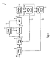
- Figure 1 shows a block diagram of the relevant units of a receiver according to this invention. It comprises a coarse VGA unit 2, a fine VGA unit 3, a clock recovery (CR) 4, a sampler 5, an ADC 6, a digital equalizer 7 and a fine logic unit 8 and a coarse logic unit 9.
- the input signal 10 that is input into the coarse VGA unit 2 represents the transmitted signal as distorted by the channel at the receiver end. It may be the output signal of an antenna in the case of radio communication or the output signal from an optical-to-electrical interface in the case of optical data transmission.
- the signal at the input of the clock recovery circuit 4 must be strong enough. However, it is even more critical to provide sampler 5 and ADC 6 with a signal having optimal strength in order to arrive at a minimum BER. To this end coarse and fine VGA 2 and 3 amplify the input signal and generate a gain controlled signal 12 which is input into CR circuit 4 and sampler 5. CR circuit 4 recovers the symbol clock and provides control signals on lines 13 and 11 to sampler 5 and ADC 6. These control signals already have an appropriate phase relation to the gain-controlled signal 12. Such clock recovery circuits are described in "Integrated Fiber-Optic Receivers" by A. Buchwald, K. W. Martin, Kluwer Academic Publishers, 1995. It is noted that ADC 6 and sampler 5 could be reversed in sequence.
- the sampler 5 essentially comprises a sample-and-hold circuit, which samples the gain-controlled signal 12 at appropriate points in time and outputs a constant signal on line 14 to the ADC until the next sampling is performed.
- the ADC provides its output in form of digital words on line 15 to digital equalizer 7 and fine and coarse logic unit 8 and 9.
- the digital equalizer 7 preferably combats ISI and consequently provides equalizer functionality.
- the fine logic unit 8 essentially calculates statistics of the digital words provided by the ADC 6 and generates a fine gain control signal on line 18 to control the gain of fine VGA 3.
- the coarse logic unit 9 operates in a similar fashion and generates a coarse gain control signal on line 19 to control the gain of coarse VGA 2. The operation of the coarse and fine logic unit 8 and 9 will be explained in more detail below. Two embodiments of fine logic unit 8 are shown in figures 2a and 2b .
- sampler 5 and ADC 6 may perform over-sampling.
- digital equalizer 7 may reduce the over-sampled digital words to one digital word per symbol and provide this data on line 20 to logic units 8 and 9 or alternatively the over-sampled digital words may be processed directly by the logic units.
- ADC 6 has 2 n quantization levels, where each sample is represented by n bits.
- the subscript i of the digital word a i represent the amplitude level of the quantized sample in value order, i.e. a 1 ⁇ a 2 ⁇ ... ⁇ a 2 n.
- the DSP counts the occurrences of each possible word, by using 2 n counters.
- M is the number of all words in this interval and T is the symbol period being the reciprocal of the symbol rate of transmission, f.
- the coarse AGC utilizes a coarse gain parameter m c indicating the amplified output signal strength.
- S c ⁇ a 2 n ⁇ .
- S c ⁇ a 1
- the coarse logic unit 9 compares the parameter m c with one or more thresholds and generates a signal for reducing or increasing the coarse gain accordingly. Consequently, the coarse AGC ensures that the signal has sufficient power, in the specified limits.
- the fine AGC 2 will be adjusted by a uniformity parameter m u , indicating the uniformity of the distribution of discrete amplitudes.
- m u uniformity parameter
- kq should be chosen as M/I.
- better performance may possibly be achieved with a slightly non-uniform choice of values kq.
- minimum BER can be achieved by minimizing the uniformity parameter m u .
- An inappropriate selection of parameters can lead to local minima, which make it hard to find the best gain value, producing the lowest number of errors.
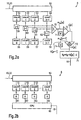
- Figure 2a shows a possible implementation of fine logic unit 8.
- Figure 2a shows a distribution circuit 50, counters 51 to 54, absolute difference circuits 59 to 62, registers 55 to 58, adder 70, comparator 72, holding circuits 71 and 74, exclusive-OR (XOR) gate 73 and fine gain calculation circuit 75.
- the digital words provided by ADC 6 on line 15 or digital equalizer on line 20 are input into distribution circuit 50.
- Distribution circuit 50 compares each digital word to a plurality of digital values the digital words may assume in order to associate each digital word to one of the subsets S q , 1 ⁇ q ⁇ l. To each of the subsets S q one of the counters 51 to 54 is associated.
- Distribution circuit 50 generates a clock pulse for every digital word it receives in order to increment the counter associated with the subset to which the digital word belongs. Additionally, for each subset one absolute difference circuit and one register is provided. Each of the absolute difference circuits calculates the absolute value of the difference of the counter value minus the register value of the counter and the register to which the absolute difference circuit is connected to. In each of the registers one number k q , 1 ⁇ q ⁇ l is stored. Adder 70 adds the outputs of all absolute difference circuits. Consequently, distribution circuit 50, counters 51 to 54, absolute difference circuits 59 to 62, registers 55 to 58 and adder 70 implement equation (5). Therefore, the output of adder 70 constitutes the uniformity parameter m u .
- the counters 51 to 54 count M digital words input into distribution circuit 50 during a period of MT wherein T is the symbol period. Then a uniformity parameter m u [p] is calculated at time tp and the counters are reset.
- the calculation of the uniformity parameter m u may take some idle time T i during which digital words are ignored on lines 15 or 20. If T i is different from 0, T i must be added to MT but, for simplicity, it is assumed to be 0 in the following discussion.
- Comparator 72 compares the newly calculated uniformity parameter m u [p] with the previously calculated uniformity parameter m u [p-1] in order to output control signal c[p] ⁇ -1,1 ⁇ . Control signal c[p] is input into XOR circuit 73.
- Timing signal b[p] is fed back to the other input of XOR circuit 73 via holding circuit 74 in order to delay timing signal b[p] by MT. Consequently the XOR circuit 73 XORs c[p] and b[p-1].
- Table 1 depicts its functionality. Table 1: functionality of XOR circuit 73 c[p] b[p-1] b[p] -1 -1 1 -1 1 -1 1 -1 1 1 1 1 1 1
- this circuit adjusts the gain in a way that the uniformity parameter m u dithers around its minimum.
- Equation (6) fg[p-1] represents the previous or old fine gain control signal and ⁇ represents an adjustment step of the fine gain control signal. Equation (6) is implemented in fine gain calculation circuit 75.
- the fine gain control signal fg is provided via line 18 to fine VGA 3 which updates the gain. After some fine gain adjustments, the gain range will be reached, and subsequently tracked, which corresponds to the minimum uniformity parameter m u and BER.
- XOR circuit 73 may be a conventional logic circuit inputting either logic 1s or 0s and outputting 0s or 1s.
- equation 6 must be modified in that previous fine gain control signal fg[p-1] is increased by ⁇ if b[p] is 1 and previous fine gain control signal fg[p-1] is decreased by ⁇ if b[p] is equivalent to 0 in fine gain calculation circuit 75.
- Fig. 2b shows a second embodiment of fine logic unit 8.
- the elements 55 to 75 are replaced by holding circuits 81, 82, 83, 84 and microprocessor 85.
- the counter values are stored in holding circuits 81 to 84.
- the counters are reset and are ready for processing the next M samples.
- Microprocessor 85 then reads out the values of the holding circuits 81 to 84 and calculates a uniformity parameter m u in compliance with equation (5). Then the microprocessor performs the functionality of holding circuit 71, comparator 72, XOR circuit 73, holding circuit 74 and fine gain calculation circuit 75 as described in connection with Fig. 2a .
- microprocessor 85 has to perform not only a single operation in order to calculate equation (5) and perform the minimum search a substantial difference in operation speed of roughly a factor 1200 remains for M equivalent to 120000 provided that the processing of the counter values takes 100 microprocessor clock cycles. So even for high-speed applications a general-purpose microprocessor 85 having a moderate clock frequency can be used.
- the application of standard microprocessors reduces development costs and receiver costs especially for small batch sizes.
- the holding circuits 81 to 84 may be omitted if microprocessor 85 is quick enough to enter all counter values within a short time or a certain number of samples are discarded in an idle period T i between the blocks of M samples which are counted. In the idle period the microprocessor 85 may read out the counter values.
- the counter values are read out by microprocessor 85 one after another in a distance smaller than MT/I. Then each counter value is reset. In this embodiment the periods of time each counter evaluates are shifted with respect to each other. Since it is assumed that the symbols do not appear in a certain pattern but rather are statistically independent this shift may be acceptable.
- the quantized samples may be directly input into a microprocessor which performs the function of elements 50 to 75 shown in Fig. 2a .
- a microprocessor which performs the function of elements 50 to 75 shown in Fig. 2a .
- Such a circuit structure can be applied only to moderate transfer rates due to operation speed limitation of the microprocessor 85.
- counters 51 to 54 may be implemented simply by registers which are incremented by an adder logic.
- subsampling may be performed, i. e. not each sample but rather only e.g. each second or third sample is processed and counted.
- Figure 3 shows a statistic of digitized sample values in the form of a bar graph.
- the possible digital words 21 are plotted on the x-axis. It is assumed that ADC 6 performs a 3-bit digitization. As a consequence the possible digital words range from 0 to 7.
- the area 23 of each bar illustrates the number of occurrences of a specific digital word within a sequence of M digital words. Such a statistic could be obtained if one counter is provided for each digital word.
- Figure 4 illustrates counter values for the statistics of Figure 3 for a first subset.
- the set S of all possible digital words is subdivided into four subsets 22.
- the first subset S 1 comprises the digital words 0 and 1, the second subset S 2 the digital words 2 and 3, the third subset digital words 4 and 5 and the fourth subset the digital words 6 and 7.
- the area of the bars having a solid upper boundary represents the counter value of a counter for the respective subset.
- the area of the bar for subset S 1 in Figure 4 should be equivalent to the area of the bars for digital words 0 and 1 in Figure 3 .
- the broken lines 24 more specifically the area of the bars defined by the broken lines, illustrates the constant values k 1 , k 2 , k 3 , k 4 which are subtracted from the counter values in order to obtain difference values.
- the absolute values of the difference values are added in order to obtain the uniformity parameter m u .
- the absolute values of the difference values are represented by the area of the stripes 26 between the solid and the broken lines.
- Figure 5 illustrates the choice of two subsets in a further embodiment of this invention.
- the set S of possible digital values is subdivided into an outer subset S 1 , 41 and an inner subset S 2 , 42.
- the outer subset S 1 comprises the digital words 0, 1, 6 and 7 whereas the inner subset S 2 comprises the digital words 2 to 5.
- the inner subset is chosen in a manner that the absolute difference between any digital word comprised in the inner subset and the average of all digital words is smaller than the absolute difference between any digital word comprised in the outer subset and the average.
- the average of all digital words in the example explained in connection with Figures 3 to 5 is 4.
- the area of bars 43 and 45 represents the count of digital words within the first subset and the area of bar 44 represents the count of digital words in the second subset.
- the broken lines 46 represent an offset k 1 .
- the uniformity parameter m u defined by equation 7 may assume both, positive and negative values. In a preferred embodiment in each adjustment step, the fine gain is changed by a value proportional to the uniformity parameter. Provided that the offset value k 1 is not too big, this is tantamount to saying that the amplification is increased if the count associated with the inner subset is greater than the count of the outer subset.
- the uniformity parameter defined in equation 7 is suitable for being processed by a proportional-integral-differential controller or a fuzzy controller since no minimum search is required.
- the performance of the method has been simulated for the case of an optical channel distorted by chromatic dispersion and noise.
- a MLSE algorithm has been applied for digital equalization, and the parameters utilized in simulation have been selected as:
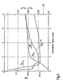
- the simulation results are shown in Fig. 6 .
- the coarse gain parameter m c , the uniformity parameter m u and the BER are plotted against the normalized signal power.
- the digital equalizer 7 produces high BER due to existing unoccupied outer quantization levels.
- the sequence estimator arrives at the region of the best BER for normalized signal power between 0.6 and 1.2.
- the gain of the coarse VGA unit 2 is adjusted first by increasing the coarse gain from lower to higher values. After the m c exceeds M/8 the coarse gain is kept constant and the fine AGC unit minimizes the uniformity parameter m u and provides the best signal power indicating the minimum BER.
- the existence of the m u minimum enables the AGC to deliver useful amplitude statistics for the downstream digital equalizer.
- Problems of signal-to-noise ratio reduction with undistorted, almost ideal channels are obviated by the coarse AGC and especially by the lower bound on m c .
- the coarse AGC will keep the signal power in some range and the fine AGC will be switched off practically.
- the fine AGC could really be switched off with the advantage of less dither penalty. Nevertheless, for time-variant channels with distortion the fine AGC demonstrates its performance.
Landscapes
- Engineering & Computer Science (AREA)
- Theoretical Computer Science (AREA)
- Control Of Amplification And Gain Control (AREA)
- Analogue/Digital Conversion (AREA)
- Circuits Of Receivers In General (AREA)
Claims (4)
- Verfahren zum Steuern der Verstärkung in einem Empfänger (1) mit:Einstellen der Verstärkung eines Verstärkers mit variabler Verstärkung (3) der ein Eingabesignal (10) verstärkt um ein verstärkungsgesteuertes Signal (12) zu erhalten;Analog-digital-wandeln (6) des verstärkungsgesteuerten Signals (12), wobei digitale Wörter (15, 20) erzeugt werden, wobei jedes digitale Wort einen Wert aus einer Vielzahl von möglichen digitalen Werten aufweist;Zählen von digitalen Wörtern, die einen Wert innerhalb einer ersten Teilmenge (S1) von möglichen digitalen Werten haben, wobei ein erster Zählerwert (51) erzeugt wird, wobei die gezählten digitalen Wörter zu einer vorbestimmten Menge von digitalen Wörtern gehören und die erste Teilmenge (S1) mindestens einen Wert enthält;Zählen (52, 53, 54) von digitalen Wörtern, die einen Wert innerhalb einer zweiten Teilmenge (S2, S3, S4) von möglichen digitalen Werten haben, wobei ein zweiter Zählerwert erzeugt wird, wobei die gezählten digitalen Wörter zu der vorbestimmten Menge von digitalen Wörtern gehören und die zweite Teilmenge sich von der ersten Teilmenge unterscheidet, wobei die zweite Teilmenge mindestens einen Wert enthält; undgekennzeichnet durchSubtrahieren eines Werts (24, 55, 56, 58) von jedem Zählerwert (25, 51, 52, 53, 54), um Differenzwerte (26) zu erhalten; undSummieren der absoluten Werte aller dieser Differenzwerte, um einen Einheitlichkeitsparameter zu erhalten; undEinstellen der Verstärkung (8, 18) um den Einheitlichkeitsparameter zu minimieren.
- Verfahren gemäß Anspruch 1, dadurch gekennzeichnet, dass jede Teilmenge mindestens zwei mögliche Digitalwerte beinhaltet.
- Schaltung zur Verwendung innerhalb eines Empfängers mit:einem Verstärker mit variabler Verstärkung (3) zum Empfangen eines analogen Signals und Ausgeben eines gesteuerten Signals (12);einem Analog-Digital-Wandler (6), der mit dem variablen Schaltverstärker (3) verbunden ist, zum Digitalisieren des verstärkungsgesteuerten Signals, wobei digitale Wörter erzeugt werden, wobei jedes digitale Wort einen Wert aus einer Vielzahl von möglichen Digitalwerten aufweist;einem ersten Zähler (51), der mit dem Analog-Digital-Wandler (6) verbunden ist, zum Zählen der digitalen Wörter, die einen Wert innerhalb einer ersten Teilmenge von möglichen Digitalwerten haben, wobei die gezählten digitalen Wörter zu einer vorbestimmten Menge von digitalen Wörtern gehören und die besagte erste Teilmenge (S1, 41) mindestens einen Wert enthält;einem zweiten Zähler (52, 53, 54), der mit dem Analog-Digital-Wandler (8) verbunden ist, zum Zählen der digitalen Wörter, die einen Wert innerhalb einer zweiten Teilmenge (S2, S3, S4, 42) von möglichen Digitalwerten haben, wobei die gezählten digitalen Wörter zur vorbestimmten Menge von digitalen Wörtern gehören, wobei die zweite Teilmenge (S2, S3, S4, 42) sich von der ersten Teilmenge (S1; 41) unterscheidet und wobei die zweite Teilmenge mindestens einen Wert enthält; undgekennzeichnet ist durch:ein erstes Register (55);ein zweites Register (56, 57, 58);eine erste Absolutdifferenzschaltung (59), die mit dem ersten Zähler (51) und dem ersten Register (55) verbunden ist, zum Berechnen der absoluten Differenz zwischen dem Wert des ersten Zählers (51) und dem Wert, der im ersten Register (55) gespeichert ist,eine zweite Absolutdifferenzschaltung (60, 61, 62), die mit dem zweiten Zähler (52, 53, 54) und dem zweiten Register (56, 57, 58) verbunden ist, zum Berechnen der absoluten Differenz zwischen dem Wert des zweiten Zählers (52, 53, 54) und dem Wert, der im zweiten Register (56, 57, 58) gespeichert ist; undeinen Addierer (70), der mit jeder der Absolutdifferenzschaltungen (59, 60, 61, 62) verbunden ist, zum Addieren der absoluten Differenzen, wobei der Addierer (70) seine Ausgabe aneine Verstärkungsberechnungsschaltung (75) liefert, die die Verstärkung gemäß der Ausgabe, die von dem Addierer (70) geliefert wurde,in einer Art und Weise, dass die Ausgabe, die durch den Addierer geliefert wird, minimiert wird, einstellt.
- Schaltung gemäß Anspruch 3, dadurch gekennzeichnet, dass sie ferner einen Addierer (70) enthält, der mit jedem der Zähler verbunden ist, um die Zählerwerte zu addieren, wobei der Addierer (70) seine Ausgabe an die Verstärkungsberechnungsschaltung (75) liefert, die die Verstärkung gemäß dem Ausgabesignal der Addiereinrichtung (70) bringt.
Priority Applications (1)
| Application Number | Priority Date | Filing Date | Title |
|---|---|---|---|
| EP04729098A EP1654802B1 (de) | 2003-04-28 | 2004-04-23 | Verfahren und schaltung zur verstärkungsregelung |
Applications Claiming Priority (3)
| Application Number | Priority Date | Filing Date | Title |
|---|---|---|---|
| EP03009564A EP1473831A1 (de) | 2003-04-28 | 2003-04-28 | Verfahren und Schaltung zur Verstärkungsregelung |
| PCT/EP2004/004337 WO2004098051A1 (en) | 2003-04-28 | 2004-04-23 | Method and circuit for controlling amplification |
| EP04729098A EP1654802B1 (de) | 2003-04-28 | 2004-04-23 | Verfahren und schaltung zur verstärkungsregelung |
Publications (2)
| Publication Number | Publication Date |
|---|---|
| EP1654802A1 EP1654802A1 (de) | 2006-05-10 |
| EP1654802B1 true EP1654802B1 (de) | 2010-07-07 |
Family
ID=32981763
Family Applications (2)
| Application Number | Title | Priority Date | Filing Date |
|---|---|---|---|
| EP03009564A Withdrawn EP1473831A1 (de) | 2003-04-28 | 2003-04-28 | Verfahren und Schaltung zur Verstärkungsregelung |
| EP04729098A Expired - Lifetime EP1654802B1 (de) | 2003-04-28 | 2004-04-23 | Verfahren und schaltung zur verstärkungsregelung |
Family Applications Before (1)
| Application Number | Title | Priority Date | Filing Date |
|---|---|---|---|
| EP03009564A Withdrawn EP1473831A1 (de) | 2003-04-28 | 2003-04-28 | Verfahren und Schaltung zur Verstärkungsregelung |
Country Status (6)
| Country | Link |
|---|---|
| US (1) | US7319363B2 (de) |
| EP (2) | EP1473831A1 (de) |
| JP (1) | JP4614940B2 (de) |
| AT (1) | ATE473550T1 (de) |
| DE (1) | DE602004028021D1 (de) |
| WO (1) | WO2004098051A1 (de) |
Families Citing this family (14)
| Publication number | Priority date | Publication date | Assignee | Title |
|---|---|---|---|---|
| EP1494413A1 (de) | 2003-07-02 | 2005-01-05 | CoreOptics, Inc., c/o The Corporation Trust Center | Kanal- und Folgeschätzung zum Empfang optischer Signale |
| US7496162B2 (en) * | 2004-11-30 | 2009-02-24 | Stmicroelectronics, Inc. | Communication system with statistical control of gain |
| JP4584062B2 (ja) * | 2005-07-21 | 2010-11-17 | セイコーインスツル株式会社 | 携帯型電子機器 |
| EP1956744A1 (de) | 2007-02-12 | 2008-08-13 | CoreOptics, Inc., c/o The Corporation Trust Center | Ausläuferextrapolator und Verfahren |
| US7880542B1 (en) * | 2007-10-03 | 2011-02-01 | Analog Devices, Inc. | Incremental gain amplifier |
| JP5001781B2 (ja) * | 2007-10-16 | 2012-08-15 | 日立アロカメディカル株式会社 | 超音波診断装置のゲイン調整方法および装置 |
| JP5088131B2 (ja) * | 2007-12-28 | 2012-12-05 | 富士通株式会社 | 電力制御回路及び電力制御方法 |
| US8451949B2 (en) * | 2008-10-07 | 2013-05-28 | Realtek Semiconductor Corp. | Clock-data recovery and method for binary signaling using low resolution ADC |
| US8391349B1 (en) * | 2009-11-12 | 2013-03-05 | Applied Micro Circuits Corporation | Equalizer with automatic gain control (AGC) |
| KR101502079B1 (ko) * | 2011-07-05 | 2015-03-13 | 삼성탈레스 주식회사 | 오버샘플링을 이용한 자동이득 제어장치 및 이를 이용한 자동이득 제어방법 |
| GB2498938A (en) * | 2012-01-31 | 2013-08-07 | Texas Instruments Ltd | Automatic gain control in a data receiver |
| CN107947811B (zh) * | 2017-12-21 | 2023-09-08 | 上海迦美信芯通讯技术有限公司 | 一种增益调节控制方法及装置 |
| CN113015233B (zh) * | 2021-05-25 | 2021-08-10 | 杭州优智联科技有限公司 | 一种自动增益控制方法、装置、设备及计算机存储介质 |
| CN114204949B (zh) * | 2021-11-30 | 2024-01-30 | 西南电子技术研究所(中国电子科技集团公司第十研究所) | 大动态快速数字agc控制方法 |
Family Cites Families (17)
| Publication number | Priority date | Publication date | Assignee | Title |
|---|---|---|---|---|
| US3931584A (en) * | 1974-09-12 | 1976-01-06 | Hycom Incorporated | Automatic gain control |
| JPS59144218A (ja) * | 1983-02-08 | 1984-08-18 | Nippon Telegr & Teleph Corp <Ntt> | 多値識別器 |
| JPS6272227A (ja) * | 1985-09-26 | 1987-04-02 | Fujitsu Ltd | 自動利得制御回路 |
| JPH0463005A (ja) * | 1990-07-02 | 1992-02-28 | Canon Inc | 自動ゲイン制御装置 |
| JPH07263986A (ja) * | 1994-03-22 | 1995-10-13 | Fujitsu Ten Ltd | 自動利得制御装置 |
| US5680075A (en) * | 1995-05-31 | 1997-10-21 | Casio Phonemate, Inc. | Digital automatic gain control |
| JP3211644B2 (ja) * | 1995-11-08 | 2001-09-25 | 松下電器産業株式会社 | 自動利得制御回路 |
| JP3120737B2 (ja) * | 1996-08-23 | 2000-12-25 | 日本電気株式会社 | 自動利得制御回路 |
| US6038435A (en) * | 1997-12-24 | 2000-03-14 | Nortel Networks Corporation | Variable step-size AGC |
| JP3329264B2 (ja) * | 1998-04-06 | 2002-09-30 | 日本電気株式会社 | Agc回路 |
| US6417730B1 (en) * | 2000-11-29 | 2002-07-09 | Harris Corporation | Automatic gain control system and related method |
| US6870891B2 (en) * | 2000-12-21 | 2005-03-22 | Intel Corporation | Low latency for start of initial automatic gain control for data in digital signal processing |
| JP2002290176A (ja) * | 2001-03-28 | 2002-10-04 | Canon Inc | 利得制御装置、無線通信装置、利得制御方法及び記憶媒体 |
| US6657488B1 (en) * | 2001-07-03 | 2003-12-02 | Silicon Laboratories, Inc. | Offset correction and slicing level adjustment for amplifier circuits |
| JP2003115774A (ja) * | 2001-10-05 | 2003-04-18 | Hitachi Ltd | 信号レベル制御を有する無線通信装置 |
| US6753727B2 (en) * | 2002-06-13 | 2004-06-22 | Skyworks Solutions, Inc. | Sequential DC offset correction for amplifier chain |
| JP2004153718A (ja) * | 2002-10-31 | 2004-05-27 | Samsung Yokohama Research Institute Co Ltd | Agc制御回路及びagc増幅器制御方法 |
-
2003
- 2003-04-28 EP EP03009564A patent/EP1473831A1/de not_active Withdrawn
-
2004
- 2004-04-23 DE DE602004028021T patent/DE602004028021D1/de not_active Expired - Lifetime
- 2004-04-23 EP EP04729098A patent/EP1654802B1/de not_active Expired - Lifetime
- 2004-04-23 US US10/554,889 patent/US7319363B2/en not_active Expired - Fee Related
- 2004-04-23 AT AT04729098T patent/ATE473550T1/de not_active IP Right Cessation
- 2004-04-23 WO PCT/EP2004/004337 patent/WO2004098051A1/en not_active Ceased
- 2004-04-23 JP JP2006505244A patent/JP4614940B2/ja not_active Expired - Fee Related
Also Published As
| Publication number | Publication date |
|---|---|
| DE602004028021D1 (de) | 2010-08-19 |
| US7319363B2 (en) | 2008-01-15 |
| ATE473550T1 (de) | 2010-07-15 |
| JP2006524939A (ja) | 2006-11-02 |
| US20070109053A1 (en) | 2007-05-17 |
| WO2004098051A1 (en) | 2004-11-11 |
| EP1473831A1 (de) | 2004-11-03 |
| EP1654802A1 (de) | 2006-05-10 |
| JP4614940B2 (ja) | 2011-01-19 |
Similar Documents
| Publication | Publication Date | Title |
|---|---|---|
| US7319363B2 (en) | Method and circuit for controlling amplification | |
| EP1645093B1 (de) | Kanal- und folgeschätzung zum empfang optischer signale | |
| EP1588517B1 (de) | Verfahren und Gerät zur automatischen Verstärkungssteuerung eines Mehrträgersignals in einem Kommunikationsempfänger | |
| US7483500B2 (en) | Narrowband gain control of receiver with digital post filtering | |
| US4775988A (en) | Method for rapid gain acquisition in a modem receiver | |
| EP1468495A1 (de) | Verfahren und vorrichtung zum optimieren des dynamikumfangs eines breitband-analog/digital-umsetzers | |
| US20040097209A1 (en) | Automatic gain control apparatus and methods | |
| CN1043236A (zh) | 数字自动增益控制技术 | |
| US10218398B2 (en) | Method and apparatus for adaptive automatic gain control | |
| US20030193423A1 (en) | Clock and data recovery with a feedback loop to adjust the slice level of an input sampling circuit | |
| US6965658B1 (en) | Method and means for telecommunication | |
| US20160218734A1 (en) | Dual threshold automatic gain control system and method | |
| JPH10215176A (ja) | A/d変換装置 | |
| EP1633050B1 (de) | Analog/Digital-Wandler mit einstellbaren Schwellwerten | |
| US7277510B1 (en) | Adaptation algorithm based on signal statistics for automatic gain control | |
| EP2249532A2 (de) | Optische Empfangsvorrichtung und optisches Empfangsverfahren | |
| EP1382121B1 (de) | Verfahren und system zur einstellung einer schwellensteuerung in einem analog/digital-umsetzer | |
| Sun et al. | Automatic gain control for ADC-limited communication | |
| WO2006124168A1 (en) | Digital automatic gain control method and device | |
| WO2008098934A1 (en) | Tail extrapolator and method | |
| JP2003218651A (ja) | 自動利得制御装置 | |
| US12556151B1 (en) | Digital control of analog amplification gain in a receiver device | |
| EP1443697A1 (de) | Bitfehlerschätzungsverfahren für einen Empfänger und Empfangsgerät | |
| EP1244246A1 (de) | Regelung der Phase eines Abtasttaktes in Empfängern |
Legal Events
| Date | Code | Title | Description |
|---|---|---|---|
| PUAI | Public reference made under article 153(3) epc to a published international application that has entered the european phase |
Free format text: ORIGINAL CODE: 0009012 |
|
| 17P | Request for examination filed |
Effective date: 20060306 |
|
| AK | Designated contracting states |
Kind code of ref document: A1 Designated state(s): AT BE BG CH CY CZ DE DK EE ES FI FR GB GR HU IE IT LI LU MC NL PL PT RO SE SI SK TR |
|
| DAX | Request for extension of the european patent (deleted) | ||
| RIN1 | Information on inventor provided before grant (corrected) |
Inventor name: LANGENBACH, STEFAN Inventor name: STOJANOVIC, NEBOJSA |
|
| 17Q | First examination report despatched |
Effective date: 20080416 |
|
| GRAP | Despatch of communication of intention to grant a patent |
Free format text: ORIGINAL CODE: EPIDOSNIGR1 |
|
| RAP1 | Party data changed (applicant data changed or rights of an application transferred) |
Owner name: COREOPTICS, INC., |
|
| GRAS | Grant fee paid |
Free format text: ORIGINAL CODE: EPIDOSNIGR3 |
|
| GRAA | (expected) grant |
Free format text: ORIGINAL CODE: 0009210 |
|
| AK | Designated contracting states |
Kind code of ref document: B1 Designated state(s): AT BE BG CH CY CZ DE DK EE ES FI FR GB GR HU IE IT LI LU MC NL PL PT RO SE SI SK TR |
|
| REG | Reference to a national code |
Ref country code: GB Ref legal event code: FG4D |
|
| REG | Reference to a national code |
Ref country code: CH Ref legal event code: EP |
|
| REG | Reference to a national code |
Ref country code: IE Ref legal event code: FG4D |
|
| REF | Corresponds to: |
Ref document number: 602004028021 Country of ref document: DE Date of ref document: 20100819 Kind code of ref document: P |
|
| REG | Reference to a national code |
Ref country code: NL Ref legal event code: VDEP Effective date: 20100707 |
|
| PG25 | Lapsed in a contracting state [announced via postgrant information from national office to epo] |
Ref country code: SI Free format text: LAPSE BECAUSE OF FAILURE TO SUBMIT A TRANSLATION OF THE DESCRIPTION OR TO PAY THE FEE WITHIN THE PRESCRIBED TIME-LIMIT Effective date: 20100707 |
|
| PG25 | Lapsed in a contracting state [announced via postgrant information from national office to epo] |
Ref country code: NL Free format text: LAPSE BECAUSE OF FAILURE TO SUBMIT A TRANSLATION OF THE DESCRIPTION OR TO PAY THE FEE WITHIN THE PRESCRIBED TIME-LIMIT Effective date: 20100707 Ref country code: AT Free format text: LAPSE BECAUSE OF FAILURE TO SUBMIT A TRANSLATION OF THE DESCRIPTION OR TO PAY THE FEE WITHIN THE PRESCRIBED TIME-LIMIT Effective date: 20100707 Ref country code: FI Free format text: LAPSE BECAUSE OF FAILURE TO SUBMIT A TRANSLATION OF THE DESCRIPTION OR TO PAY THE FEE WITHIN THE PRESCRIBED TIME-LIMIT Effective date: 20100707 |
|
| PG25 | Lapsed in a contracting state [announced via postgrant information from national office to epo] |
Ref country code: PT Free format text: LAPSE BECAUSE OF FAILURE TO SUBMIT A TRANSLATION OF THE DESCRIPTION OR TO PAY THE FEE WITHIN THE PRESCRIBED TIME-LIMIT Effective date: 20101108 Ref country code: PL Free format text: LAPSE BECAUSE OF FAILURE TO SUBMIT A TRANSLATION OF THE DESCRIPTION OR TO PAY THE FEE WITHIN THE PRESCRIBED TIME-LIMIT Effective date: 20100707 Ref country code: CY Free format text: LAPSE BECAUSE OF FAILURE TO SUBMIT A TRANSLATION OF THE DESCRIPTION OR TO PAY THE FEE WITHIN THE PRESCRIBED TIME-LIMIT Effective date: 20100707 Ref country code: BG Free format text: LAPSE BECAUSE OF FAILURE TO SUBMIT A TRANSLATION OF THE DESCRIPTION OR TO PAY THE FEE WITHIN THE PRESCRIBED TIME-LIMIT Effective date: 20101007 |
|
| PG25 | Lapsed in a contracting state [announced via postgrant information from national office to epo] |
Ref country code: BE Free format text: LAPSE BECAUSE OF FAILURE TO SUBMIT A TRANSLATION OF THE DESCRIPTION OR TO PAY THE FEE WITHIN THE PRESCRIBED TIME-LIMIT Effective date: 20100707 Ref country code: SE Free format text: LAPSE BECAUSE OF FAILURE TO SUBMIT A TRANSLATION OF THE DESCRIPTION OR TO PAY THE FEE WITHIN THE PRESCRIBED TIME-LIMIT Effective date: 20100707 Ref country code: GR Free format text: LAPSE BECAUSE OF FAILURE TO SUBMIT A TRANSLATION OF THE DESCRIPTION OR TO PAY THE FEE WITHIN THE PRESCRIBED TIME-LIMIT Effective date: 20101008 |
|
| RAP2 | Party data changed (patent owner data changed or rights of a patent transferred) |
Owner name: CISCO TECHNOLOGY, INC. |
|
| PG25 | Lapsed in a contracting state [announced via postgrant information from national office to epo] |
Ref country code: DK Free format text: LAPSE BECAUSE OF FAILURE TO SUBMIT A TRANSLATION OF THE DESCRIPTION OR TO PAY THE FEE WITHIN THE PRESCRIBED TIME-LIMIT Effective date: 20100707 |
|
| PLBE | No opposition filed within time limit |
Free format text: ORIGINAL CODE: 0009261 |
|
| STAA | Information on the status of an ep patent application or granted ep patent |
Free format text: STATUS: NO OPPOSITION FILED WITHIN TIME LIMIT |
|
| PG25 | Lapsed in a contracting state [announced via postgrant information from national office to epo] |
Ref country code: IT Free format text: LAPSE BECAUSE OF FAILURE TO SUBMIT A TRANSLATION OF THE DESCRIPTION OR TO PAY THE FEE WITHIN THE PRESCRIBED TIME-LIMIT Effective date: 20100707 Ref country code: SK Free format text: LAPSE BECAUSE OF FAILURE TO SUBMIT A TRANSLATION OF THE DESCRIPTION OR TO PAY THE FEE WITHIN THE PRESCRIBED TIME-LIMIT Effective date: 20100707 Ref country code: CZ Free format text: LAPSE BECAUSE OF FAILURE TO SUBMIT A TRANSLATION OF THE DESCRIPTION OR TO PAY THE FEE WITHIN THE PRESCRIBED TIME-LIMIT Effective date: 20100707 Ref country code: EE Free format text: LAPSE BECAUSE OF FAILURE TO SUBMIT A TRANSLATION OF THE DESCRIPTION OR TO PAY THE FEE WITHIN THE PRESCRIBED TIME-LIMIT Effective date: 20100707 Ref country code: RO Free format text: LAPSE BECAUSE OF FAILURE TO SUBMIT A TRANSLATION OF THE DESCRIPTION OR TO PAY THE FEE WITHIN THE PRESCRIBED TIME-LIMIT Effective date: 20100707 |
|
| 26N | No opposition filed |
Effective date: 20110408 |
|
| PG25 | Lapsed in a contracting state [announced via postgrant information from national office to epo] |
Ref country code: ES Free format text: LAPSE BECAUSE OF FAILURE TO SUBMIT A TRANSLATION OF THE DESCRIPTION OR TO PAY THE FEE WITHIN THE PRESCRIBED TIME-LIMIT Effective date: 20101018 |
|
| REG | Reference to a national code |
Ref country code: DE Ref legal event code: R081 Ref document number: 602004028021 Country of ref document: DE Owner name: CISCO TECHNOLOGY, INC., US Free format text: FORMER OWNER: COREOPTICS, INC., WILMINGTON, US Effective date: 20110427 Ref country code: DE Ref legal event code: R081 Ref document number: 602004028021 Country of ref document: DE Owner name: CISCO TECHNOLOGY, INC., SAN JOSE, US Free format text: FORMER OWNER: COREOPTICS, INC., WILMINGTON, US Effective date: 20110427 |
|
| REG | Reference to a national code |
Ref country code: GB Ref legal event code: 732E Free format text: REGISTERED BETWEEN 20110609 AND 20110615 |
|
| REG | Reference to a national code |
Ref country code: DE Ref legal event code: R097 Ref document number: 602004028021 Country of ref document: DE Effective date: 20110408 |
|
| PG25 | Lapsed in a contracting state [announced via postgrant information from national office to epo] |
Ref country code: MC Free format text: LAPSE BECAUSE OF NON-PAYMENT OF DUE FEES Effective date: 20110430 |
|
| REG | Reference to a national code |
Ref country code: CH Ref legal event code: PL |
|
| PG25 | Lapsed in a contracting state [announced via postgrant information from national office to epo] |
Ref country code: CH Free format text: LAPSE BECAUSE OF NON-PAYMENT OF DUE FEES Effective date: 20110430 Ref country code: LI Free format text: LAPSE BECAUSE OF NON-PAYMENT OF DUE FEES Effective date: 20110430 |
|
| REG | Reference to a national code |
Ref country code: IE Ref legal event code: MM4A |
|
| PG25 | Lapsed in a contracting state [announced via postgrant information from national office to epo] |
Ref country code: IE Free format text: LAPSE BECAUSE OF NON-PAYMENT OF DUE FEES Effective date: 20110423 |
|
| PG25 | Lapsed in a contracting state [announced via postgrant information from national office to epo] |
Ref country code: LU Free format text: LAPSE BECAUSE OF NON-PAYMENT OF DUE FEES Effective date: 20110423 |
|
| PG25 | Lapsed in a contracting state [announced via postgrant information from national office to epo] |
Ref country code: TR Free format text: LAPSE BECAUSE OF FAILURE TO SUBMIT A TRANSLATION OF THE DESCRIPTION OR TO PAY THE FEE WITHIN THE PRESCRIBED TIME-LIMIT Effective date: 20100707 |
|
| PG25 | Lapsed in a contracting state [announced via postgrant information from national office to epo] |
Ref country code: HU Free format text: LAPSE BECAUSE OF FAILURE TO SUBMIT A TRANSLATION OF THE DESCRIPTION OR TO PAY THE FEE WITHIN THE PRESCRIBED TIME-LIMIT Effective date: 20100707 |
|
| REG | Reference to a national code |
Ref country code: DE Ref legal event code: R082 Ref document number: 602004028021 Country of ref document: DE Representative=s name: HASELTINE LAKE LLP, DE |
|
| REG | Reference to a national code |
Ref country code: FR Ref legal event code: PLFP Year of fee payment: 13 |
|
| REG | Reference to a national code |
Ref country code: FR Ref legal event code: PLFP Year of fee payment: 14 |
|
| REG | Reference to a national code |
Ref country code: FR Ref legal event code: PLFP Year of fee payment: 15 |
|
| PGFP | Annual fee paid to national office [announced via postgrant information from national office to epo] |
Ref country code: DE Payment date: 20200429 Year of fee payment: 17 Ref country code: FR Payment date: 20200427 Year of fee payment: 17 |
|
| PGFP | Annual fee paid to national office [announced via postgrant information from national office to epo] |
Ref country code: GB Payment date: 20200427 Year of fee payment: 17 |
|
| REG | Reference to a national code |
Ref country code: DE Ref legal event code: R082 Ref document number: 602004028021 Country of ref document: DE Representative=s name: HL KEMPNER PATENTANWALT, RECHTSANWALT, SOLICIT, DE |
|
| REG | Reference to a national code |
Ref country code: DE Ref legal event code: R119 Ref document number: 602004028021 Country of ref document: DE |
|
| GBPC | Gb: european patent ceased through non-payment of renewal fee |
Effective date: 20210423 |
|
| PG25 | Lapsed in a contracting state [announced via postgrant information from national office to epo] |
Ref country code: FR Free format text: LAPSE BECAUSE OF NON-PAYMENT OF DUE FEES Effective date: 20210430 Ref country code: GB Free format text: LAPSE BECAUSE OF NON-PAYMENT OF DUE FEES Effective date: 20210423 Ref country code: DE Free format text: LAPSE BECAUSE OF NON-PAYMENT OF DUE FEES Effective date: 20211103 |
|
| P01 | Opt-out of the competence of the unified patent court (upc) registered |
Effective date: 20230525 |