EP1655838A2 - Correcteur de linéarité avec multiplication de filtres - Google Patents
Correcteur de linéarité avec multiplication de filtres Download PDFInfo
- Publication number
- EP1655838A2 EP1655838A2 EP05256742A EP05256742A EP1655838A2 EP 1655838 A2 EP1655838 A2 EP 1655838A2 EP 05256742 A EP05256742 A EP 05256742A EP 05256742 A EP05256742 A EP 05256742A EP 1655838 A2 EP1655838 A2 EP 1655838A2
- Authority
- EP
- European Patent Office
- Prior art keywords
- order
- filter
- signal
- filter product
- linearity corrector
- Prior art date
- Legal status (The legal status is an assumption and is not a legal conclusion. Google has not performed a legal analysis and makes no representation as to the accuracy of the status listed.)
- Granted
Links
- 238000000034 method Methods 0.000 claims abstract description 7
- 230000003111 delayed effect Effects 0.000 claims 5
- 238000012545 processing Methods 0.000 abstract description 11
- 239000000047 product Substances 0.000 description 28
- 238000012937 correction Methods 0.000 description 10
- 238000010586 diagram Methods 0.000 description 5
- 238000001914 filtration Methods 0.000 description 4
- 230000007246 mechanism Effects 0.000 description 4
- 230000001934 delay Effects 0.000 description 3
- 238000013461 design Methods 0.000 description 3
- 238000005259 measurement Methods 0.000 description 3
- 230000000694 effects Effects 0.000 description 2
- 238000001228 spectrum Methods 0.000 description 2
- 239000006227 byproduct Substances 0.000 description 1
- 238000006243 chemical reaction Methods 0.000 description 1
- 238000000354 decomposition reaction Methods 0.000 description 1
- 230000001419 dependent effect Effects 0.000 description 1
- 230000008030 elimination Effects 0.000 description 1
- 238000003379 elimination reaction Methods 0.000 description 1
- 238000012886 linear function Methods 0.000 description 1
- 230000009022 nonlinear effect Effects 0.000 description 1
- 238000005457 optimization Methods 0.000 description 1
- 238000012856 packing Methods 0.000 description 1
- 238000007670 refining Methods 0.000 description 1
- 238000004088 simulation Methods 0.000 description 1
- 235000013599 spices Nutrition 0.000 description 1
- 238000012549 training Methods 0.000 description 1
Images


Classifications
-
- H—ELECTRICITY
- H03—ELECTRONIC CIRCUITRY
- H03M—CODING; DECODING; CODE CONVERSION IN GENERAL
- H03M1/00—Analogue/digital conversion; Digital/analogue conversion
- H03M1/06—Continuously compensating for, or preventing, undesired influence of physical parameters
- H03M1/0617—Continuously compensating for, or preventing, undesired influence of physical parameters characterised by the use of methods or means not specific to a particular type of detrimental influence
- H03M1/0626—Continuously compensating for, or preventing, undesired influence of physical parameters characterised by the use of methods or means not specific to a particular type of detrimental influence by filtering
-
- H—ELECTRICITY
- H03—ELECTRONIC CIRCUITRY
- H03M—CODING; DECODING; CODE CONVERSION IN GENERAL
- H03M1/00—Analogue/digital conversion; Digital/analogue conversion
- H03M1/12—Analogue/digital converters
Definitions
- the present invention relates to linearity error correction, and more particularly to a linearity corrector using filter products to reduce, or eliminate, distortion generated by signal processing systems, such as an analog to digital converter (ADC).
- ADC analog to digital converter
- SFDR spurious-free dynamic range
- Modem high-speed ADC designs use a deep clock pipeline to help accurately convert an analog input to a sampled digital representation in a series of refining steps.
- the ADC designers make significant efforts to remove obvious sources of nonlinearities in the analog processing circuits. However, it is typically difficult to remove all sources of errors.
- Designers tend to remove the most obvious problems of the circuit until computerized modeling, for example SPICE modeling, shows that the converter meets specifications. Linearity can be improved using techniques such as reducing dynamic range at the nonlinear device, or using feedback around it.
- some circuit topologies have inherent distortion mechanisms that cannot be completely removed.
- Pipelined processing also provides opportunities for internal digital and analog circuit activity to modulate the processing of internal analog signals.
- the residual nonlinear distortion is generated by self-modulation of the input signal with a linear function of itself or its own derivative. This results in some lower level distortions that are hard to eliminate. Such modulation could occur via the internal power supply distribution.
- the number of circuit paths that can generate voltage modulation on the power supply rails may be quite high. Simulating these effects complicates device modeling, and slows computerized simulations. To first order, these contributions to power supply modulation will add almost linearly, so they can be modeled as a linear finite impulse response (FIR) filter.
- FIR linear finite impulse response
- modulation occurs, which corresponds to a multiplication.
- modulation typically occurs in the high gain analog amplifiers between conversion stages.
- the harmonic and intermodulation distortion is typically characterized by the presence of 2 nd and 3 rd order distortion terms, with very little higher-order distortion occurring.
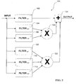
- Fig. 1 illustrates a version of this solution having a 1 st order correction and a 3 rd order correction.
- the first order compensation is provided by filter 12 ( h 1 ).
- the 3 rd order compensation is provided by multiplying the output of filter 14 and the output of filter 16 using the multiplier 18, filtering the output from the multiplier 18 using filter 20, multiplying the output of filter 20 with the output of filter 22 using multiplier 24 and finally filtering the output of the multiplier 24 using filter 26.
- a linear cubic compensation may be provided.
- This implementation utilizes filter 20 after multiplier 18, and filter 26 after multiplier 24. Once the linear cubic compensation is obtained, it is subtracted from the output of the unknown system that is being compensated. This requires that the corrector have access to the original signal that was input into the unknown system, which is not available where the original signal is not digital. While it may be a useful subcase of a Volterra filter, it has drawbacks that make it unsuitable for systems with a good linear frequency response. The filters following the multipliers cannot distinguish between original components and aliased components caused by the nonlinear effects of the prior multiplications.
- aliasing does not allow the filter to correct for differences in phase and amplitude response between the original and aliased components when used in applications that use most of a Nyquist band.
- a remaining problem in linearity compensation systems relates to calibration. These systems may require solving for systems of filter coefficients that are nonlinear with respect to the output. Solving for more coefficients requires more computation for any calibration scheme that can be applied to the system.
- Embodiments of the present ADC linear correctors can be implemented using far fewer filter taps than systems based upon general purpose Volterra filter systems.
- the ADC output can be passed through a digital processing network that distorts the signal in substantially the same way, and then subtracts the distortion to reduce, or eliminate, the ADC distortion.
- this method improves the spurious-free dynamic range (SFDR) of an ADC.
- SFDR spurious-free dynamic range
- an ADC with an SFDR of 80dB may be improved by a factor of 15dB, depending upon the ADC characteristics.
- This improvement also removes some filters from prior proposed topologies, thereby simplifying the design for use with systems that have a relatively flat linear frequency response. This simplification can be traded off for longer filters in the correction system, thereby obtaining improved performance with the same amount of processing.
- the improvement is significant for precision measurement applications, such as those associated with spectrum analyzers, oscilloscopes, or other measurement instruments that use ADCs.
- a linearity corrector having a first order signal path for passing a first order signal having higher order distortion, an n th order filter product circuit, where n is an integer greater than 1, providing a compensating signal having a delay relative to the first order signal path, and an adder connected to the first signal path and directly connected to the n th order filter product circuit such that the compensating signal reduces the corresponding distortion terms in the first order signal.
- the method of compensation provides a filter product that is simply summed with a relative delay to a first order signal path such that distortion components in an original output from an ADC are reduced, or eliminated.
- Fig. 1 is a block diagram of a prior art linearity corrector arrangement for compensating loud speakers.
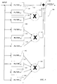
- Fig. 2 is a block diagram of a filter product based linearity corrector including compensation for 1 st , 2 nd , and 3 rd order distortions.
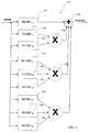
- Fig. 3 is a block diagram of a filter product based linearity corrector including compensation for 1 st and 3 rd order distortions.
- Fig. 4 is a block diagram of a filter product based linearity corrector including compensation for 1 st , 3 rd , and 4 th order distortions.
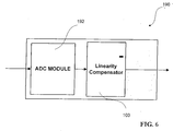
- Fig. 5 is a block diagram of a compensated ADC.
- Volterra filter coefficients are linear with output y , so a set of h can, in theory, be found with training data.
- Embodiments of the present ADC linearity corrector rely on a subset of a Volterra filter system.
- the system order n defines a set of product orders k for 1 ⁇ k ⁇ n .
- the correction model has the same form, except that the order, and filter lengths are chosen beforehand, based on experimentation with a particular ADC architecture. Calibration then involves finding the filter taps. Note that the filter taps will, in general, be different for each filter.
- FIG. 2 illustrates an embodiment of a linearity corrector 100 for implementing Eq. 5.
- the output of a signal processing system such as an ADC, is provided as the input to the linearity corrector 100.
- Each of the linear convolutions, as provided in Eq. 5, is implemented using filters 102 through 112.
- the filters may be implemented as FIR filters.
- the first order term corresponds to the filter 102.
- the first order term is achieved by replacing the filter 102 with a fixed delay equal to approximately half the lengths of the other filters.
- the first order term is achieved by replacing the filter 102 with the combination of a fixed delay and a filter, such that the fixed delay plus half the filter length is approximately half the length of the other order filters.
- the second order term is implemented by multiplying the outputs from filter 104 and filter 106 using a multiplier 120 to produce a 2 nd order filter product.
- the third order is implemented by multiplying the outputs from filter 108, filter 110 and filter 112 using multiplier 122 to produce a 3 rd order filter product.
- the output from the filter 102 is then added to the output from the multiplier 120 and the multiplier 122 using the adder 124 to provide a simple sum of the filter products as an output.
- the term simple sum as used herein refers to the operation of adding the multiplier values without additional filtering between the multipliers and the adder 124. This simple sum is achieved by directly connecting the multipliers to the adder.
- directly connecting means that there are no filters or other processing elements in the path, there may be registers or other elements in the path that do not change the sample values of the signal data on the path.
- the output is now a compensated signal with reduced nonlinearities that were produced by the signal processing system, such as an ADC.
- embodiments of the present invention have eliminated the filters following the multipliers, which were provided in prior art solutions. While this may require filters having additional taps as compared to the prior art shown in Fig. 1, it allows the filters to perform a better job of tracking variations in the ADC as a function of frequency. For example, if the prior art of Fig.
- longer length filters may increase the number of variables to solve for during calibration, which tends to slow down the calibration algorithm.
- longer length filters may also require additional delays to match the filter signal delays. Accordingly, in an embodiment of the corrector 100, all of the filter lengths are equal so that no additional delays are needed.
- Fig. 3 illustrates an embodiment of a linearity corrector 100 designed to compensate for 1 st order and 3 rd order distortion, without compensating for 2 nd order distortion.
- second order distortion may not be significant enough to justify inclusion of 2 nd order compensation.
- the 3 rd order compensation is provided by multiplying the outputs from filter 108, filter 110 and filter 112 using multiplier 122 to produce a 3 rd order filter product.
- the simple sum of the 3 rd order filter product and the first order filter product may then provide a compensated signal having reduced, or eliminated, 1 st and 3 rd order distortions.
- Fig. 5 shows a filter product system designed to compensate for two 3 rd order distortions. Since each product order k may only compensate for a single self-modultion mechanism, by providing two 3 rd order filter products it may be possible to compensate for two 3 rd order distortions. Accordingly, a second 3 rd order filter product is obtained by multiplying filter 160, filter 162, and filter 164 using multiplier 166. This second 3 rd order filter product may then be added to the first 3 rd order filter product from multiplier 122 using the adder 124.
- the various embodiments of the linearity corrector 100 may be implemented using dedicated hardware, such as an FPGA or an ASIC, or using a general purpose processor running software.
- the FPGA or ASIC are useful for performing real-time correction, while software running on a general purpose processor would be useful for post-acquisition correction.
- software on a general purpose processor for real-time correction, as well.
- the linearity corrector 100 is used to compensate a signal output from an ADC
- the structure of the linearity corrector 100 may be integrated within the same packing, or possibly on the same chip as the ADC, in order to form a compensated ADC.
- the compensated ADC 190 is shown in Fig. 6. It comprises the ADC module 192, which contains the various circuits to convert an analog signal into a digital signal.
- the digital output of the ADC module 192 is input into the linearity corrector 100, which may implemented as taught above.
- the output of the linearity corrector is an output having reduced harmonic and intermodulation distortion. This combined structure provides a corrected ADC.
Landscapes
- Engineering & Computer Science (AREA)
- Theoretical Computer Science (AREA)
- Analogue/Digital Conversion (AREA)
- Amplifiers (AREA)
- Cable Transmission Systems, Equalization Of Radio And Reduction Of Echo (AREA)
- Noise Elimination (AREA)
Priority Applications (1)
| Application Number | Priority Date | Filing Date | Title |
|---|---|---|---|
| EP08003174A EP1933459A1 (fr) | 2004-11-04 | 2005-10-31 | Correcteur de linéarité utilisant des produits de filtres |
Applications Claiming Priority (2)
| Application Number | Priority Date | Filing Date | Title |
|---|---|---|---|
| US62537204P | 2004-11-04 | 2004-11-04 | |
| US11/258,030 US7348908B2 (en) | 2004-11-04 | 2005-10-26 | Linearity corrector using filter products |
Related Child Applications (1)
| Application Number | Title | Priority Date | Filing Date |
|---|---|---|---|
| EP08003174A Division EP1933459A1 (fr) | 2004-11-04 | 2005-10-31 | Correcteur de linéarité utilisant des produits de filtres |
Publications (3)
| Publication Number | Publication Date |
|---|---|
| EP1655838A2 true EP1655838A2 (fr) | 2006-05-10 |
| EP1655838A3 EP1655838A3 (fr) | 2006-06-14 |
| EP1655838B1 EP1655838B1 (fr) | 2009-06-17 |
Family
ID=36168910
Family Applications (1)
| Application Number | Title | Priority Date | Filing Date |
|---|---|---|---|
| EP05256742A Ceased EP1655838B1 (fr) | 2004-11-04 | 2005-10-31 | Correcteur de linéarité avec multiplication de filtres |
Country Status (4)
| Country | Link |
|---|---|
| US (1) | US7348908B2 (fr) |
| EP (1) | EP1655838B1 (fr) |
| JP (1) | JP4754941B2 (fr) |
| DE (1) | DE602005014922D1 (fr) |
Cited By (1)
| Publication number | Priority date | Publication date | Assignee | Title |
|---|---|---|---|---|
| GB2541379A (en) * | 2015-08-14 | 2017-02-22 | Csir | Method and system for improving spurious free dynamic range of signal processing systems |
Families Citing this family (23)
| Publication number | Priority date | Publication date | Assignee | Title |
|---|---|---|---|---|
| RU2333592C2 (ru) * | 2006-10-30 | 2008-09-10 | Олег Григорьевич Светников | Способ обеспечения допустимой величины частотных искажений усилителя и устройство для его осуществления |
| US8913652B2 (en) * | 2008-03-10 | 2014-12-16 | Newlans, Inc. | Method, system and apparatus for wideband signal processing |
| US8655936B2 (en) * | 2008-06-23 | 2014-02-18 | Kapik Inc. | System and method for processing a signal with a filter employing FIR and IIR elements |
| US8866531B2 (en) | 2010-02-12 | 2014-10-21 | Newlans, Inc. | Broadband analog radio-frequency integrator |
| WO2012061385A1 (fr) | 2010-11-01 | 2012-05-10 | Newlans, Inc. | Procédé et appareil de linéarisation d'amplificateur de puissance |
| US8970252B2 (en) | 2010-11-08 | 2015-03-03 | Newlans, Inc. | Field programmable analog array |
| JP5653319B2 (ja) | 2011-08-15 | 2015-01-14 | 株式会社東芝 | 歪み補正装置 |
| JP2015502688A (ja) | 2011-11-01 | 2015-01-22 | ニューランズ・インコーポレーテッドNewlans,Inc. | 広帯域信号の処理 |
| WO2014039517A1 (fr) | 2012-09-05 | 2014-03-13 | Newlans, Inc. | Etalonnage biquadratique |
| US9031177B2 (en) * | 2012-12-20 | 2015-05-12 | Broadcom Corporation | Digital calibration of analog distortion using split analog front-end |
| JP6182869B2 (ja) * | 2013-01-16 | 2017-08-23 | オンキヨー株式会社 | 音声再生装置 |
| CN105553904B (zh) * | 2015-12-09 | 2019-01-15 | 西安星通通信科技有限公司 | 一种数字信号幅度和相位校准方法及系统 |
| US10547942B2 (en) | 2015-12-28 | 2020-01-28 | Samsung Electronics Co., Ltd. | Control of electrodynamic speaker driver using a low-order non-linear model |
| US10462565B2 (en) | 2017-01-04 | 2019-10-29 | Samsung Electronics Co., Ltd. | Displacement limiter for loudspeaker mechanical protection |
| US10506347B2 (en) | 2018-01-17 | 2019-12-10 | Samsung Electronics Co., Ltd. | Nonlinear control of vented box or passive radiator loudspeaker systems |
| US10701485B2 (en) | 2018-03-08 | 2020-06-30 | Samsung Electronics Co., Ltd. | Energy limiter for loudspeaker protection |
| WO2020025164A1 (fr) * | 2018-07-30 | 2020-02-06 | Sew-Eurodrive Gmbh & Co. Kg | Procédé pour faire fonctionner un système d'entraînement et système d'entraînement |
| US10542361B1 (en) | 2018-08-07 | 2020-01-21 | Samsung Electronics Co., Ltd. | Nonlinear control of loudspeaker systems with current source amplifier |
| US11012773B2 (en) | 2018-09-04 | 2021-05-18 | Samsung Electronics Co., Ltd. | Waveguide for smooth off-axis frequency response |
| US10797666B2 (en) | 2018-09-06 | 2020-10-06 | Samsung Electronics Co., Ltd. | Port velocity limiter for vented box loudspeakers |
| US11265093B2 (en) * | 2020-06-29 | 2022-03-01 | U-Blox Ag | Method and device for group delay variation compensation |
| US11356773B2 (en) | 2020-10-30 | 2022-06-07 | Samsung Electronics, Co., Ltd. | Nonlinear control of a loudspeaker with a neural network |
| JP7556459B2 (ja) * | 2020-11-25 | 2024-09-26 | 日本電信電話株式会社 | 波形等化器、波形等化方法および波形等化プログラム |
Family Cites Families (11)
| Publication number | Priority date | Publication date | Assignee | Title |
|---|---|---|---|---|
| US4019997A (en) * | 1974-02-04 | 1977-04-26 | General Electric Company | Silicone fluid useful as a brae fluid |
| US4606538A (en) * | 1985-04-04 | 1986-08-19 | Wang Kuo L | Physical exercise device |
| US5308296A (en) * | 1992-07-16 | 1994-05-03 | Donald Eckstein | Interactive video and exercise apparatus |
| JPH0662284A (ja) * | 1992-08-04 | 1994-03-04 | Sharp Corp | 雑音除去装置 |
| US5594612A (en) * | 1994-08-24 | 1997-01-14 | Crystal Semiconductor Corporation | Analog-to-digital converter with digital linearity correction |
| JP2000253486A (ja) * | 1999-02-26 | 2000-09-14 | Victor Co Of Japan Ltd | 二次歪み付加装置 |
| US6639537B1 (en) * | 2000-03-31 | 2003-10-28 | Massachusetts Institute Of Technology | Highly linear analog-to-digital conversion system and method thereof |
| US6570514B1 (en) * | 2001-12-21 | 2003-05-27 | Scott R. Velazquez | Linearity error compensator |
| JP4033794B2 (ja) * | 2003-03-24 | 2008-01-16 | 株式会社エヌ・ティ・ティ・ドコモ | 高効率線形電力増幅器 |
| US6911925B1 (en) * | 2004-04-02 | 2005-06-28 | Tektronix, Inc. | Linearity compensation by harmonic cancellation |
| US20070123390A1 (en) * | 2005-11-29 | 2007-05-31 | Mathis Christopher E | Exercise equipment with interactive gaming component |
-
2005
- 2005-10-26 US US11/258,030 patent/US7348908B2/en not_active Expired - Fee Related
- 2005-10-31 DE DE602005014922T patent/DE602005014922D1/de not_active Expired - Lifetime
- 2005-10-31 EP EP05256742A patent/EP1655838B1/fr not_active Ceased
- 2005-11-04 JP JP2005321544A patent/JP4754941B2/ja not_active Expired - Fee Related
Non-Patent Citations (5)
| Title |
|---|
| FRANK W ET AL: "Realtime Loudspeaker Linearization" IEEE WINTER WORKSHOP ON NONLINEAR DIGITAL SIGNAL PROCESSING, 1993, 17 January 1993 (1993-01-17), pages 2.1.3.1-2.1.3.5, XP010334788 Tampere, Finland * |
| FRANK W: "Compensation of linear and nonlinear sensor distortions by digital post processing" PROCEEDINGS 7TH INTERNATIONAL CONFERENCE FOR SENSORS TRANSDUCERS AND SYSTEMS (SENSOR 95), 1995, pages 889-892, XP002363900 Germany * |
| KARAGIANNI K ET AL INSTITUTE OF ELECTRICAL AND ELECTRONICS ENGINEERS: "Efficient third-order volterra filter computation in the time domain" CONFERENCE RECORD OF THE 37TH. ASILOMAR CONFERENCE ON SIGNALS, SYSTEMS, & COMPUTERS. PACIFIC GROOVE, CA, NOV. 9 - 12, 2003, ASILOMAR CONFERENCE ON SIGNALS, SYSTEMS AND COMPUTERS, NEW YORK, NY : IEEE, US, vol. VOL. 1 OF 2. CONF. 37, 9 November 2003 (2003-11-09), pages 2180-2184, XP010702671 ISBN: 0-7803-8104-1 * |
| KOH T ET AL: "Second-order Volterra filtering and its application to nonlinear system identification" IEEE TRANSACTIONS ON ACOUSTICS, SPEECH AND SIGNAL PROCESSING USA, vol. ASSP-33, no. 6, December 1985 (1985-12), pages 1445-1455, XP002363898 ISSN: 0096-3518 * |
| ZHANG JIA-SHU ET AL: "A reduced parameter second-order Volterra filter with application to nonlinear adaptive prediction of chaotic time series" ACTA PHYSICA SINICA CHINESE PHYS. SOC CHINA, vol. 50, no. 7, 2001, pages 1248-1254, XP009060153 ISSN: 1000-3290 * |
Cited By (1)
| Publication number | Priority date | Publication date | Assignee | Title |
|---|---|---|---|---|
| GB2541379A (en) * | 2015-08-14 | 2017-02-22 | Csir | Method and system for improving spurious free dynamic range of signal processing systems |
Also Published As
| Publication number | Publication date |
|---|---|
| EP1655838B1 (fr) | 2009-06-17 |
| DE602005014922D1 (de) | 2009-07-30 |
| US7348908B2 (en) | 2008-03-25 |
| JP4754941B2 (ja) | 2011-08-24 |
| EP1655838A3 (fr) | 2006-06-14 |
| JP2006135993A (ja) | 2006-05-25 |
| US20060092057A1 (en) | 2006-05-04 |
Similar Documents
| Publication | Publication Date | Title |
|---|---|---|
| US7348908B2 (en) | Linearity corrector using filter products | |
| CN1998140B (zh) | 一种失真补偿模数转换器及补偿方法 | |
| US9564876B2 (en) | Digital compensation for a non-linear analog receiver | |
| US9945901B1 (en) | Measuring and correcting non-idealities of a system | |
| US8825415B2 (en) | Methods and apparatuses for estimation and compensation on nonlinearity errors | |
| Wang et al. | Joint blind calibration for mixed mismatches in two-channel time-interleaved ADCs | |
| EP1583243B1 (fr) | Compensation de linéarité par annulation des signaux harmoniques | |
| CN106685424A (zh) | 用于模数转换器的微处理器辅助校准 | |
| US11652491B2 (en) | High-pass shaped dither in continuous-time residue generation systems for analog-to-digital converters | |
| US7161515B2 (en) | Calibration system and method for a linearity corrector using filter products | |
| US8410960B2 (en) | Method to linearize the output from an ADC | |
| CN1815893B (zh) | 利用滤波器乘积的线性校正器 | |
| Wang et al. | Digital estimation and compensation method for nonlinearity mismatches in time-interleaved analog-to-digital converters | |
| Soudan et al. | Correction structures for linear weakly time-varying systems | |
| EP1933459A1 (fr) | Correcteur de linéarité utilisant des produits de filtres | |
| Wang et al. | Bandwidth-efficient calibration method for nonlinear errors in M-channel time-interleaved ADCs | |
| Zhao et al. | Correlation-based reconfigurable blind calibration for timing mismatches in TI-ADCs | |
| US12445144B2 (en) | Continuous-time ADC calibration techniques | |
| Deng et al. | Efficient Parallel Polynomial-Based Compensation Structure for Frequency Response Mismatch in Two-Channel TI-ADCs | |
| US20190013828A1 (en) | Method and system for improving spurious free dynamic range of signal processing systems | |
| US9112457B1 (en) | Decompressor |
Legal Events
| Date | Code | Title | Description |
|---|---|---|---|
| PUAI | Public reference made under article 153(3) epc to a published international application that has entered the european phase |
Free format text: ORIGINAL CODE: 0009012 |
|
| AK | Designated contracting states |
Kind code of ref document: A2 Designated state(s): AT BE BG CH CY CZ DE DK EE ES FI FR GB GR HU IE IS IT LI LT LU LV MC NL PL PT RO SE SI SK TR |
|
| AX | Request for extension of the european patent |
Extension state: AL BA HR MK YU |
|
| PUAL | Search report despatched |
Free format text: ORIGINAL CODE: 0009013 |
|
| AK | Designated contracting states |
Kind code of ref document: A3 Designated state(s): AT BE BG CH CY CZ DE DK EE ES FI FR GB GR HU IE IS IT LI LT LU LV MC NL PL PT RO SE SI SK TR |
|
| AX | Request for extension of the european patent |
Extension state: AL BA HR MK YU |
|
| 17P | Request for examination filed |
Effective date: 20061206 |
|
| AKX | Designation fees paid |
Designated state(s): DE FR GB IT |
|
| 17Q | First examination report despatched |
Effective date: 20070321 |
|
| APBN | Date of receipt of notice of appeal recorded |
Free format text: ORIGINAL CODE: EPIDOSNNOA2E |
|
| APBR | Date of receipt of statement of grounds of appeal recorded |
Free format text: ORIGINAL CODE: EPIDOSNNOA3E |
|
| APBV | Interlocutory revision of appeal recorded |
Free format text: ORIGINAL CODE: EPIDOSNIRAPE |
|
| GRAP | Despatch of communication of intention to grant a patent |
Free format text: ORIGINAL CODE: EPIDOSNIGR1 |
|
| GRAS | Grant fee paid |
Free format text: ORIGINAL CODE: EPIDOSNIGR3 |
|
| GRAA | (expected) grant |
Free format text: ORIGINAL CODE: 0009210 |
|
| AK | Designated contracting states |
Kind code of ref document: B1 Designated state(s): DE FR GB IT |
|
| REG | Reference to a national code |
Ref country code: GB Ref legal event code: FG4D |
|
| REF | Corresponds to: |
Ref document number: 602005014922 Country of ref document: DE Date of ref document: 20090730 Kind code of ref document: P |
|
| PLBE | No opposition filed within time limit |
Free format text: ORIGINAL CODE: 0009261 |
|
| STAA | Information on the status of an ep patent application or granted ep patent |
Free format text: STATUS: NO OPPOSITION FILED WITHIN TIME LIMIT |
|
| 26N | No opposition filed |
Effective date: 20100318 |
|
| REG | Reference to a national code |
Ref country code: FR Ref legal event code: PLFP Year of fee payment: 11 |
|
| REG | Reference to a national code |
Ref country code: FR Ref legal event code: PLFP Year of fee payment: 12 |
|
| REG | Reference to a national code |
Ref country code: FR Ref legal event code: PLFP Year of fee payment: 13 |
|
| PGFP | Annual fee paid to national office [announced via postgrant information from national office to epo] |
Ref country code: FR Payment date: 20171025 Year of fee payment: 13 |
|
| PGFP | Annual fee paid to national office [announced via postgrant information from national office to epo] |
Ref country code: IT Payment date: 20171024 Year of fee payment: 13 |
|
| PGFP | Annual fee paid to national office [announced via postgrant information from national office to epo] |
Ref country code: DE Payment date: 20181029 Year of fee payment: 14 |
|
| PGFP | Annual fee paid to national office [announced via postgrant information from national office to epo] |
Ref country code: GB Payment date: 20181029 Year of fee payment: 14 |
|
| PG25 | Lapsed in a contracting state [announced via postgrant information from national office to epo] |
Ref country code: FR Free format text: LAPSE BECAUSE OF NON-PAYMENT OF DUE FEES Effective date: 20181031 |
|
| PG25 | Lapsed in a contracting state [announced via postgrant information from national office to epo] |
Ref country code: IT Free format text: LAPSE BECAUSE OF NON-PAYMENT OF DUE FEES Effective date: 20181031 |
|
| REG | Reference to a national code |
Ref country code: DE Ref legal event code: R119 Ref document number: 602005014922 Country of ref document: DE |
|
| PG25 | Lapsed in a contracting state [announced via postgrant information from national office to epo] |
Ref country code: DE Free format text: LAPSE BECAUSE OF NON-PAYMENT OF DUE FEES Effective date: 20200501 |
|
| GBPC | Gb: european patent ceased through non-payment of renewal fee |
Effective date: 20191031 |
|
| PG25 | Lapsed in a contracting state [announced via postgrant information from national office to epo] |
Ref country code: GB Free format text: LAPSE BECAUSE OF NON-PAYMENT OF DUE FEES Effective date: 20191031 |