EP1655952A2 - Dispositif de prise d'images à l'état solide, sa méthode de commande et appareil de prise d'images - Google Patents
Dispositif de prise d'images à l'état solide, sa méthode de commande et appareil de prise d'images Download PDFInfo
- Publication number
- EP1655952A2 EP1655952A2 EP05023689A EP05023689A EP1655952A2 EP 1655952 A2 EP1655952 A2 EP 1655952A2 EP 05023689 A EP05023689 A EP 05023689A EP 05023689 A EP05023689 A EP 05023689A EP 1655952 A2 EP1655952 A2 EP 1655952A2
- Authority
- EP
- European Patent Office
- Prior art keywords
- signal charges
- columns
- unit
- vertical transfer
- predetermined number
- Prior art date
- Legal status (The legal status is an assumption and is not a legal conclusion. Google has not performed a legal analysis and makes no representation as to the accuracy of the status listed.)
- Granted
Links
Images


Classifications
-
- H—ELECTRICITY
- H04—ELECTRIC COMMUNICATION TECHNIQUE
- H04N—PICTORIAL COMMUNICATION, e.g. TELEVISION
- H04N25/00—Circuitry of solid-state image sensors [SSIS]; Control thereof
- H04N25/70—SSIS architectures; Circuits associated therewith
- H04N25/71—Charge-coupled device [CCD] sensors; Charge-transfer registers specially adapted for CCD sensors
- H04N25/715—Charge-coupled device [CCD] sensors; Charge-transfer registers specially adapted for CCD sensors using frame interline transfer [FIT]
-
- H—ELECTRICITY
- H04—ELECTRIC COMMUNICATION TECHNIQUE
- H04N—PICTORIAL COMMUNICATION, e.g. TELEVISION
- H04N25/00—Circuitry of solid-state image sensors [SSIS]; Control thereof
- H04N25/40—Extracting pixel data from image sensors by controlling scanning circuits, e.g. by modifying the number of pixels sampled or to be sampled
- H04N25/42—Extracting pixel data from image sensors by controlling scanning circuits, e.g. by modifying the number of pixels sampled or to be sampled by switching between different modes of operation using different resolutions or aspect ratios, e.g. switching between interlaced and non-interlaced mode
-
- H—ELECTRICITY
- H04—ELECTRIC COMMUNICATION TECHNIQUE
- H04N—PICTORIAL COMMUNICATION, e.g. TELEVISION
- H04N25/00—Circuitry of solid-state image sensors [SSIS]; Control thereof
- H04N25/40—Extracting pixel data from image sensors by controlling scanning circuits, e.g. by modifying the number of pixels sampled or to be sampled
- H04N25/44—Extracting pixel data from image sensors by controlling scanning circuits, e.g. by modifying the number of pixels sampled or to be sampled by partially reading an SSIS array
- H04N25/445—Extracting pixel data from image sensors by controlling scanning circuits, e.g. by modifying the number of pixels sampled or to be sampled by partially reading an SSIS array by skipping some contiguous pixels within the read portion of the array
-
- H—ELECTRICITY
- H04—ELECTRIC COMMUNICATION TECHNIQUE
- H04N—PICTORIAL COMMUNICATION, e.g. TELEVISION
- H04N25/00—Circuitry of solid-state image sensors [SSIS]; Control thereof
- H04N25/40—Extracting pixel data from image sensors by controlling scanning circuits, e.g. by modifying the number of pixels sampled or to be sampled
- H04N25/44—Extracting pixel data from image sensors by controlling scanning circuits, e.g. by modifying the number of pixels sampled or to be sampled by partially reading an SSIS array
- H04N25/447—Extracting pixel data from image sensors by controlling scanning circuits, e.g. by modifying the number of pixels sampled or to be sampled by partially reading an SSIS array by preserving the colour pattern with or without loss of information
-
- H—ELECTRICITY
- H04—ELECTRIC COMMUNICATION TECHNIQUE
- H04N—PICTORIAL COMMUNICATION, e.g. TELEVISION
- H04N25/00—Circuitry of solid-state image sensors [SSIS]; Control thereof
- H04N25/40—Extracting pixel data from image sensors by controlling scanning circuits, e.g. by modifying the number of pixels sampled or to be sampled
- H04N25/46—Extracting pixel data from image sensors by controlling scanning circuits, e.g. by modifying the number of pixels sampled or to be sampled by combining or binning pixels
Definitions
- the present invention contains subject matter related to Japanese Patent Application JP 2004-315490 filed in the Japanese Patent Office on October 29, 2004, the entire contents of which are incorporated herein by reference.
- the present invention relates to solid-state imaging devices, methods for driving solid-state imaging devices, and imaging apparatuses. More specifically, the present invention relates to a charge-transfer solid-state imaging device, such as a charge-coupled-device (CCD) imaging device, a method for driving the solid-state imaging device, and an imaging apparatus, such as a digital still camera, including the charge-transfer solid-state imaging device as an imaging device.
- a charge-transfer solid-state imaging device such as a charge-coupled-device (CCD) imaging device
- CCD charge-coupled-device
- an imaging apparatus such as a digital still camera
- Imaging apparatuses e.g., digital still cameras (DSCs)
- DSCs digital still cameras
- CCD imaging devices as imaging devices.
- all-pixel-readout solid-state imaging devices signal charges of all pixels that are simultaneously read out to vertical transfer units are vertically transferred individually, rather than jointly, by the vertical transfer units, and are horizontally transferred and output by a horizontal transfer unit.
- the number of pixels in CCD imaging devices for DSCs has increased in order to increase the still image quality.
- smearing due to higher-density cells is conspicuous, and, in particular, is conspicuous in a moving-image capturing mode or a monitoring mode.
- Smearing is a phenomenon unique to CCD imaging devices in which vertical bright stripes appear in high-brightness areas of an image of an object when bright light enters vertical transfer units for transferring signal charges. The longer the signal charges remain in the vertical transfer units, the more conspicuous the smearing effect is.
- the frame interline transfer (FIT) method that is used in professional broadcast CCD imaging devices is one solution for reducing the occurrence of smearing.
- FIT-type CCD imaging devices a light-shielded accumulator for temporarily accumulating signal charges transferred by vertical transfer units is provided below an imaging unit including a matrix of pixels. The signal charges are read out from the pixels to the vertical transfer units, and are then rapidly transferred to the accumulator by the vertical transfer units performing a high-speed transfer operation. The period of time during which the signal charges remain in the vertical transfer units is reduced, thereby reducing the occurrence of smearing.
- FIT-type CCD imaging devices with accumulators lead to a large chip size, which is about 1.5 to 2 times as large as the chip size of CCD imaging devices of the interline transfer (IT) type without accumulators.
- IT interline transfer
- VGA quality 640 pixels wide by 480 pixels high
- demands for DSC CCD imaging devices including a large number of pixels have increased in order to increase the still image quality.
- demands for CCD imaging devices including more pixels an increased number of pixels lead to a large gap between the frame rate in a still-image capturing mode and the frame rate used for the vide function (including monitoring).
- One known implementation of the video function is a technique for thinning out signal charges read out from pixels in the vertical direction to increase the frame rate. For example, referring to Fig. 12, in color coding of two (horizontal) by two (vertical) pixel patterns, two pixels of each color for every 16 vertical pixels (16 lines) are read out to vertical transfer units and added in the vertical transfer units, and the signal charges of the remaining pixels are not read out (or are thinned out) (4/16-line readout).
- the amount of horizontal pixel information is excessively larger than the amount of vertical pixel information, which is uneconomical, and there is no balance between the vertical resolution and the horizontal resolution.
- the number of vertical pixels to be thinned out is reduced to increase the amount of pixel information, thereby preventing the occurrence of smearing or the generation of false-color signals. Furthermore, in order to prevent the horizontal driving frequency (the driving frequency of the horizontal transfer unit) from increasing due to an increased amount of pixel information, pixel addition is also performed in the horizontal direction to reduce the amount of pixel information (see, for example, Japanese Unexamined Patent Application Publication No. 11-234569).
- the above-described technique of the related art can reduce the occurrence of smearing and the generation of false-color signals by increasing the amount of vertical pixel information using a combination of thinning-out and addition in the vertical direction and two-pixel addition in the horizontal direction, and can prevent the horizontal driving frequency from increasing by reducing the amount of horizontal pixel information.
- the amount of horizontal pixel information can only be reduced to 1/2 while the amount of vertical pixel information is reduced to 1/4. That is, the amount of horizontal pixel information is two times as large as the amount of vertical pixel information, and the problem of no balance between the vertical resolution and the horizontal resolution still remains.
- a solid-state imaging device includes a plurality of pixels arranged into a matrix for performing photoelectric conversion and a plurality of vertical transfer units arranged in columns for vertically transferring signal charges of the plurality of pixels on a column-by-column basis, and a horizontal transfer unit for horizontally transferring the signal charges transferred from the plurality of vertical transfer units.
- a predetermined operation mode a predetermined number of columns greater than one are used as a unit, transfer of charges from a vertical transfer unit in a predetermined column of the predetermined number of columns is stopped, and the signal charges transferred from the vertical transfer units in the remaining columns of the predetermined number of columns are added or read out to output the added or read out signal charges.
- the number of pixels to be thinned out or the number of pixels to be added can arbitrarily be set depending on the number of pixels to be thinned and added in the vertical direction to provide a good balance between the vertical resolution and the horizontal resolution and to reduce the horizontal driving frequency. Furthermore, transfer of charges of the vertical transfer unit in the column of which pixels are to be thinned out is stopped, thereby allowing the signal components and the smear components to be thinned out. No empty packets including only smear components are produced in the horizontal transfer unit, thus preventing the occurrence of smearing.
- the present invention in units of a plurality of columns of a plurality of vertical transfer units, transfer of charges from a vertical transfer unit in a predetermined column of the plurality of columns is stopped, and the signal charges transferred from the vertical transfer units in the remaining columns are added or read out to output the added or read out signal charges.
- the thinning-out and addition or thinning-output and read-out processing without the occurrence of smearing is performed in the horizontal direction to reduce the amount of horizontal pixel information. Therefore, there is a good balance between the vertical resolution and the horizontal resolution, and the horizontal driving frequency can be reduced.
- Fig. 1 is a schematic configuration diagram showing the configuration of a charge-transfer solid-state imaging device according to an embodiment of the present invention, e.g., a CCD imaging device 10.
- the CCD imaging device 10 shown in Fig. 1 has an FIT-type device configuration including, for example, an imaging unit 11 and an accumulator 12.
- the imaging unit 11 includes a matrix of pixels (photosensors including photoelectric conversion devices) 111 for converting incident light into signal charges of an amount corresponding to the amount of the incident light, and a plurality of vertical CCDs (vertical transfer units) 112 each provided for a column of pixels in the matrix of pixels 111.
- the signal charges photoelectrically converted by the pixels 111 and read out from the pixels 111 are vertically transferred on a column-by-column basis by the vertical CCDs.
- a charge controller 13 is provided between the imaging unit 11 and the accumulator 12.
- the specific configuration and operation of the charge controller 13 are discussed in detail below in the context of two embodiments.
- the accumulator 12 is a region shielded from light, and is used for temporarily accumulating the signal charges supplied via the charge controller 13.
- the vertical CCDs 112 and the charge controller 13 are driven to perform a high-speed transfer operation, and the signal charges are rapidly transferred to the accumulator 12 from the vertical CCDs 112 and the charge controller 13.
- the FIT-type CCD imaging device 10 including the accumulator 12 can reduce the period of time during which the signal charges remain in the vertical CCDs 112, and is therefore greatly effective to reduce the occurrence of smearing.
- the signal charges temporarily accumulated in the accumulator 12 are sequentially shifted (or transferred) to a horizontal CCD (horizontal transfer unit) 14.
- the horizontal CCD 14 horizontally transfers the signal charges shifted from the accumulator 12.
- the CCD imaging device 10 further includes a charge detecting unit 15 at the leading end of the horizontal CCD 14.
- the charge detecting unit 15 includes, for example, floating-diffusion amplifiers, and is adapted to convert the signal charges sequentially transferred by the horizontal CCD 14 into voltage signals and to output the signals from a port CCDout.
- the CCD imaging device 10 with the above-described configuration is driven by various timing signals generated by a timing generator (TG) 20.
- TG timing generator
- the timing generator 20 Based on a vertical synchronization signal VD, a horizontal synchronization signal HD, and a master clock MCK, the timing generator 20 generates timing signals including, for example, six-phase vertical transfer pulses IM1 to IM6 for driving the vertical CCDs 112, storage pulses Storage1 and Storage2 and hold pulses Hold1 and Hold2 for driving the charge controller 13, for example, four-phase vertical transfer pulses ST1 to ST4 for driving the accumulator 12, for example, two-phase horizontal transfer pulses H1 and H2 for driving the horizontal CCD 14.
- These timing signals are generated so as to have the timing relationship corresponding to capturing mode information supplied from the outside.
- a drain voltage Drain is supplied to the charge controller 13 from the timing generator 20.
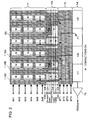
- Fig. 2 is a schematic plan pattern view showing the configuration of the main part including a charge controller 13A according to a first embodiment of the present invention.
- Color coding of a color filter (not shown) provided on the top layer of the imaging unit 11 is based on two (horizontal) by two (vertical) pixel patterns, by way of example, and the charge controller 13A performs processing in units of three columns (i.e., three horizontal pixels).
- a predetermined operation mode in units of a plurality of columns of the plurality of vertical CCDs 112, and the charge controller 13A according to the first embodiment stops transferring charges from a vertical CCD 112 in a predetermined column of the plurality of columns to thin out the charges, and adds signal charges transferred from the two or more remaining vertical CCDs 112 to output the added signal charges.
- This processing is hereinafter referred to as horizontal thinning-out and addition processing.
- the charge controller 13A converts signal charges transferred in parallel from the vertical CCDs 112 in units of the plurality of columns into serially arranged signal charges, and sequentially outputs the serially arranged signal charges.
- three vertical CCDs 112 namely, vertical CCDs 112A, 112B, and 112C, are used as a unit.
- the charge controller 13A is independently provided with storage electrodes 131B and 131C and hold electrodes 132B and 132C in each of the channels in such a manner that the storage electrodes 131B and 131C are closer to the imaging unit 11.
- the charge controller 13A is not provided with a storage electrode or a hold electrode.
- the storage electrode 131B is horizontally narrower (in width) than the storage electrode 131C, and a drain portion 133 serving as a charge drain unit is further provided in the lateral region of the storage electrode 131B.
- the charge controller 13A with the above-described configuration is driven and controlled by the control pulses generated by the timing generator 20, i.e., the storage pulses Storage1 and Storage2, the drain voltage Drain, and the hold pulses Hold1 and Hold2, to perform the horizontal thinning-out and addition processing.
- the storage pulse Storage1 is carried by a control line 134-1 to drive the storage electrode 131B
- the storage pulse Storage2 is carried by a control line 134-2 to drive the storage electrode 131C.
- the drain voltage Drain is carried by a control line 134-3 to drive the drain portion 133.
- the hold pulse Hold1 is carried by a control line 134-4 to drive the hold electrode 132B
- the hold pulse Hold2 is carried by a control line 134-5 to drive the hold electrode 132C.
- control lines 134-1 to 134-5 carrying the storage pulses Storage1 and Storage2, the drain voltage Drain, and the hold pulses Hold1 and Hold2 extend in parallel to one another across the charge controller 13A in the arrangement direction of the vertical CCDs 112 (i.e., the horizontal direction), and have a shunt configuration such that the storage electrodes 131B and 131C, the drain portion 133, the hold electrodes 132B and 132C are brought into electrical contact for every three columns.
- the storage electrode 131B and the hold electrode 132B provided for the vertical CCD 112B are driven by a combination of the storage pulse Storage1 and the hold pulse Hold1, and the storage electrode 131C and the hold electrode 132C provided for the vertical CCD 112C are driven by a combination of the storage pulse Storage2 and the hold pulse Hold2.
- the imaging unit 11, the charge controller 13A, and the accumulator 12 include channel stop regions 30, as hatched in Fig. 2.
- the charge controller 13A with the above-described configuration performs the horizontal thinning-out and addition processing in units of three columns (i.e., three horizontal pixels), by way of example, so as to support, for example, vertical three-pixel addition.
- a method for driving the CCD imaging device 10 including the charge controller 13A with the above-described configuration will now be described in the context of a moving-image capturing mode for capturing a moving image (including a monitoring mode) and a still-image capturing mode for capturing a still image.
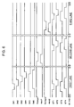
- Addition of three pixels of the same color for every other pixel is performed in the vertical direction without performing the thinning-out processing, thereby allowing for uniformity of the centroid of pixels in taking a moving image, as can be seen from equal intervals in the vertical direction between adders, indicated by typical signs in Fig. 3 for adding pixels.
- No thinning-out of pixel information prevents the generation of false-color signals.
- the processing for thinning out pixel information is not performed, no empty packets are produced during vertical transfer, thus preventing the occurrence of smearing.
- the vertical CCDs 112 (112A, 112B, and 112C) transfer the signal charges of the pixels in the bottom row of the imaging unit 11 to the charge controller 13A.
- the signal charges of the vertical CCD 112A in the first column are transferred to the accumulator 12, passing through the charge controller 13A.
- the storage pulse Storage1 is in the "H” level state so that the potential under the storage electrode 131B becomes deep, and the hold pulse Hold1 is in the "L" level state so that the potential under the hold electrode 132B becomes shallow.
- the signal charges of the vertical CCD 112B in the second column are accumulated under the storage electrode 131B, and a potential barrier produced under the hold electrode 132B stops transferring these signal charges to the accumulator 12.
- the potential barrier stops transferring not only the signal components (i.e., the signal charges) but also smear components (or smear charges).
- the accumulated charges over the potential barrier are drained to the drain portion 133 by the following vertical transfer operation.
- the storage pulse Storage2 and the hold pulse Hold2 undergo a transition from the "L" level to the "H” level in synchronization with the rising of the fifth-phase vertical transfer pulse IM5 so that the potential under the storage electrode 131C and the potential under the hold electrode 132C become deep.
- the signal charges of the vertical CCD 112A in the first column the signal charges of the vertical CCD 112C in the third column are transferred to the accumulator 12, passing through the charge controller 13A.
- the charge controller 13A stops transferring the signal charges of the middle vertical CCD 112B, and transmits the signal charges of the side vertical CCDs 112A and 112C so that the transmitted signal charges are added in the accumulator 12.
- the charge controller 13A allows the horizontal thinning-out and addition processing for thinning out the pixel information (including the smear components) of the middle column and adding the pixel information for the side columns.
- a signal charge of a B pixel is thinned out in a certain unit and signal charges of B pixels on both sides of the B pixel are added, and a signal charge of a G pixel is thinned out in the adjacent unit and signal charges of B pixels on both sides of the G pixels are added.
- the signal charges that are obtained by the charge controller 13A performing thinning-out to, for example, two third of the number of horizontal pixels, followed by addition, are vertically transferred to the horizontal CCD 14 by the four-phase (ST1 to ST4) driving in the accumulator 12.
- the signal charges are horizontally transferred by the two-phase (H1 and H2) driving to the charge detecting unit 15.
- the charge detecting unit 15 converts the signal charges into voltage signals and outputs the converted signals.
- the horizontal thinning-out and addition processing is performed, and the number of pixels to be added and the number of pixels to be thinned out can arbitrarily be set depending on the number of pixels to be added in the vertical direction to prevent the amount of horizontal image information from being excessively larger than the amount of vertical pixel information and to allow the same rate of pixel information in both directions. Therefore, there is a good balance between the horizontal resolution and the vertical resolution of a moving image.
- the first embodiment in association with vertical three-pixel addition, one pixel is thinned out for every three horizontal pixels. The amount of pixel information in the vertical and horizontal directions is therefore reduced to 1/3.
- Fig. 5 is a conceptual diagram showing vertical addition and horizontal thinning-out and addition in units of, for example, three pixels in the vertical and horizontal directions.
- pixel information of 640 (vertical) by 853 (horizontal) pixels is obtained by performing vertical and horizontal pixel addition (with the horizontal thinning-out processing) in units of three pixels.
- the centroid of pixels in both vertical and horizontal directions can also be uniform.
- the charge controller 13A provided between the imaging unit 11 and the accumulator 12 allows the signal charges of vertical CCDs 112 in the columns of which pixels are to be added, e.g., the vertical CCDs 112A and 112C, to be transmitted and added in the accumulator 12 before they are transferred to the horizontal CCD 14.
- No empty packets are produced in the horizontal CCD 14 due to no thinning-out, thus preventing the occurrence of smearing caused by addition of smear components in empty packets. That is, transfer of charges from the vertical CCD 112B of which pixels are to be thinned out is stopped to thin out the signal components and the smear components, thus preventing the occurrence of smearing.
- the pixel information for the middle column is thinned out while the pixel information for the side columns are added.
- this is merely an example, and any other form may be used.
- the color coding scheme of the color filter is not limited to color coding based on a primary-color Bayer array, and may be color coding based on a primary-color stripe array, a complementary-color lattice array, or the like.
- the number of columns used as a unit of thinning-out and addition is not limited to three but may be four or more.
- the column of which the pixel information is to be thinned out is not limited to one middle column.
- the column of which the pixel information is to be thinned out or the column of which the pixel information is to be added can be determined depending on the color coding scheme.
- the pixels of which pixel information is to be added are not limited to pixels of the same color.
- pixels of different primary colors may be added to obtain complementary-color pixel information.
- a signal processing system in the subsequent stage of the CCD imaging device 10 regenerates the original primary colors from the complementary color.
- the horizontal thinning-out and addition processing is performed in units of, for example, three columns (i.e., three horizontal pixels).
- the charge controller 13A performs processing for converting the signal charges transferred in parallel from the three vertical CCDs 112A, 112B, and 112C into serially arranged signal charges and sequentially outputting the serially arranged signal charges.
- three-line sequence is used in which signal charges of pixels in one row are read out in three blocks.
- the total processing time of the three-line sequence is substantially the same as the processing time of a sequence in which signal charges of pixels in one row of the imaging unit 11 are sequentially transferred by the accumulator 14 and the horizontal CCD 12 and are output via the charge detecting unit 15.
- the vertical CCDs 112 (112A, 112B, and 112C) transfer the signal charges of the pixels in the bottom row of the imaging unit 11 in parallel to the charge controller 13A.
- the signal charges of the vertical CCD 112A in the first column are transferred to the accumulator 12, passing through the charge controller 13A.
- the storage pulses Storage1 and Storage2 are in the "H” level state so that the potentials under the storage electrodes 131B and 131C become deep, and the hold pulses Hold1 and Hold2 are in the "L" level state so that the potentials under the hold electrodes 132B and 132C become shallow.
- the signal charges of the vertical CCDs 112B and 112C in the second and third columns are accumulated under the storage electrodes 131B and 131C, and potential barriers produced under the hold electrodes 132B and 132C stop transferring charges to the accumulator 12.
- the signal charges of the vertical CCD 112A in the first column transferred to the accumulator 12 through the charge controller 13A are vertically transferred to the horizontal CCD 14 by the four-phase (ST1 to ST4) driving in the accumulator 12.
- the signal charges are horizontally transferred by the two-phase (H1 and H2) driving to the charge detecting unit 15.
- the charge detecting unit 15 converts the signal charges into voltage signals and outputs the converted signals.
- the hold pulse Hold1 is brought to the "H” level from the “L” level so that the potential under the hold electrode 132B becomes deep, and the storage pulse Storage1 is then brought to the "L” level from the “H” level so that the potential under the storage electrode 131B becomes shallow.
- the signal charges of the vertical CCD 112B in the second column held under the storage electrode 131B are transferred to the accumulator 12, passing through the charge controller 13A.
- the signal charges of the vertical CCD 112C in the third column are still held under the storage electrode 131C.
- the signal charges of the vertical CCD 112B in the second column transferred to the accumulator 12 through the charge controller 13A are vertically transferred by the accumulator 12 to the horizontal CCD 14.
- the signal charges are horizontally transferred to the charge detecting unit 15.
- the charge detecting unit 15 converts the signal charges into voltage signals and outputs the converted signals.
- the hold pulse Hold2 brought to the H" level from the “L” level so that the potential under the hold electrode 132C becomes deep
- the storage pulse Storage2 is then brought to the "L” level from the “H” level so that the potential under the storage electrode 131C becomes shallow.
- the signal charges of the vertical CCD 112C in the third column held under the storage electrode 131C are transferred to the accumulator 12, passing through the charge controller 13A.
- the signal charges of the vertical CCD 112C in the third column transferred to the accumulator 12 through the charge controller 13A are vertically transferred by the accumulator 12 to the horizontal CCD 14.
- the signal charges are horizontally transferred to the by the charge detecting unit 15.
- the charge detecting unit 15 converts the signal charges into voltage signals, and outputs the converted signals.
- the charge controller 13A allows the signal charges of three pixels transferred in parallel in units of three vertical CCDs 112 of the imaging unit 11, i.e., the vertical CCDs 112A, 112B, and 112C, to be converted into serially arranged signal charges, which are then sequentially transferred to the accumulator 12.
- the pixel signals output after the three-line sequence are returned to the original pixel array of one row of the imaging unit 11 by the signal processing system in the subsequent stage of the CCD imaging device 10 by alternately rearranging the three-line pixel signals using a line memory or the like.
- signal charges transferred in parallel from the imaging unit 11 in units of, for example, three columns (i.e., three horizontal pixels), which are used as a unit of the horizontal thinning-out and addition processing, are converted into serially arranged signal charges by the charge controller 13A.
- the charge controller 13A used for horizontal thinning-out and addition in the moving-image capturing mode is provided between the imaging unit 11 and the accumulator 12, the signal charges of all pixels 111 of the imaging unit 11 can independently be read out by the three-line sequence.
- the charge controller 13A In case of performing the horizontal thinning-out and addition processing in units of three columns, the charge controller 13A according to the first embodiment is not provided with a storage electrode or hold electrode for the vertical CCD 112A in the first column, and transfers the signal charges of the vertical CCD 112A in the first column directly to the accumulator 12.
- the charge controller 13A may be provided with a storage electrode and a hold electrode for the vertical CCD 112A in the first column in a similar manner to that of the vertical CCDs 112B and 112C in the second and third columns, and may temporarily hold the signal charges of the vertical CCD 112A in the first column.
- the timing relation may be set so that the temporarily held signal charges of the vertical CCD 112A in the first column can first pass through the charge controller 13A.
- the storage electrode and the hold electrode provided for the vertical CCD 112A in the first column increase the complexity of the configuration and the timing control. It can be understood that no storage electrode or hold electrode provided for the vertical CCD 112A in the first column is more advantageous.
- the charge controller 13A As discussed above, in the FIT-type CCD imaging device 10 including the imaging unit 11 and the accumulator 12, the charge controller 13A according to the first embodiment is provided between the imaging unit 11 and the accumulator 12.
- the charge controller 13A performs the horizontal thinning-out and addition processing in the moving-image capturing mode
- the number of pixels to be added and to be thinned out in the horizontal direction can arbitrarily be set depending on the number of pixels to be added in the vertical direction (possibly with the thinning-out processing), thereby preventing the amount of horizontal image information from being excessively larger than the amount of vertical pixel information.
- the horizontal driving frequency can be reduced.
- pixel addition without the thinning-out processing is performed in the vertical direction, and no empty packets are produced in the vertical CCDs 112.
- the charge controller 13A used for the horizontal thinning-out and addition processing further thins out the signal components and the smear components for the vertical CCD of which pixels are to be thinned out so as not to produce empty packets in the horizontal CCD 14. In the moving-image capturing mode, therefore, the occurrence of smearing caused by pixel addition can be prevented.
- the occurrence of smearing can greatly be reduced in the video mode in cooperation with the smear reduction effect of the accumulator 12.
- the charge controller 13A performs the horizontal thinning-out and addition processing and outputs signal charges to the accumulator 12.
- the charge controller 13A converts the signal charges transferred in parallel from the imaging unit 11 in units of pixels to be subjected to the horizontal thinning-out and addition processing into serially arranged signal charges, and outputs the signal charges to the accumulator 12. Therefore, the amount of pixel information in the horizontal direction can be reduced (to 1/3 when the horizontal thinning-out and addition processing is carried out in units of three horizontal pixels), and the vertical size of the accumulator 12 can also be reduced.
- the reduction in the amount of horizontal pixel information allows the horizontal size of a packet in the accumulator 12 to be designed to be larger than the horizontal size of a pixel unit (including a pixel 111 and a vertical CCD 112 associated therewith).
- the horizontal size of the packet can be designed to be as large as the horizontal size of the three pixel units corresponding to three horizontal pixels.
- the chip size of the CCD imaging device 10 can greatly be reduced in the vertical direction.
- the vertical size of the accumulator 12 is generally about 50% larger than the vertical size of the imaging unit 11, and the chip size in the vertical direction of the CCD imaging device is about 1.5 times the vertical size of the imaging unit 11.
- the chip size of the CCD imaging device directly affects the device price.
- the FIT-type CCD imaging device is therefore too expensive to mount in a consumer imaging apparatus, e.g., a digital still camera, at the current stage.
- the horizontal size of a packet of the accumulator 12 can be designed to be as large as the size of three horizontal pixels, and the vertical size of the accumulator 12 can be reduced to about 20% of the vertical size of the imaging unit 11, for example, in a case where the horizontal thinning-out and addition processing is performed in units of three columns (i.e., three horizontal pixels) and one column of pixel (i.e., one pixel) is thinned out.
- the chip size of the CCD imaging device 10 can therefore be reduced in the vertical direction to about 1.2 times the vertical size of the imaging unit 11.
- the FIT-type CCD imaging device 10 including the charge controller 13A according to the first embodiment allows significant reduction in chip size and also allows significant reduction in cost.
- the FIT-type CCD imaging device 10 is therefore suitable to mount in a consumer imaging apparatus, e.g., a digital still camera, which is difficult in the related art in view of cost.
- the image quality can greatly be increased.
- CCD imaging devices such as IT-type CCD imaging devices without the accumulator 12, or charge-transfer solid-state imaging devices other than CCD imaging devices may be employed.
- the charge controller 13A is provided below the imaging unit 11, and, in the moving-image capturing mode, the charge controller 13A performs the horizontal thinning-out and addition processing and outputs signal charges to the horizontal CCD 14.
- the charge controller 13A converts the signal charges transferred in parallel from the imaging unit 11 in units of pixels to be subjected to the horizontal thinning-out and addition processing into serially arranged signal charges, and outputs the signal charges to the horizontal CCD 14. Therefore, there is a good balance between the horizontal resolution and the vertical resolution without the occurrence of smearing in the video mode, and the horizontal driving frequency can be reduced.
- Fig. 7 is a schematic plan pattern view showing the configuration of the main part including a charge controller 13B according to a second embodiment of the present invention.
- the portions equivalent to those shown in Fig. 2 are identified by the same reference numerals.
- Color coding of a color filter (not shown) provided on the top layer of the imaging unit 11 is based on two (horizontal) by two (vertical) pixel patterns, by way of example, and the charge controller 13B performs processing in units of four columns (i.e., four horizontal pixels).
- a predetermined operation mode a plurality of columns of the vertical CCDs 112 are used as a unit, and the charge controller 13B according to the second embodiment stops transferring charges from a vertical CCD 112 in a predetermined column of the plurality of columns to thin out the charges, and reads out the signal charges transferred from the remaining vertical CCDs 112 to the accumulator 12.
- This processing is hereinafter referred to as horizontal thinning-out and read-out processing.
- the charge controller 13A reads out the signal charges transferred in parallel in units of the plurality of columns from the plurality of vertical CCDs 112 using a multiple-line sequence, e.g., a two-line sequence.
- the charge controller 13B is provided with a storage electrode 135 and a hold electrode 136 in each of the channels so as to extend across the channels in such a manner that the storage electrode 135 is closer to the imaging unit 11.
- the charge controller 13B is not provided with a storage electrode or a hold electrode.
- the storage electrode 135 is partially cut out, and a drain portion 137 serving as a charge drain unit is provided in the cutout region of the storage electrode 135.
- the charge controller 13B with the above-described configuration is driven and controlled by the control pulses generated by the timing generator 20, i.e., the storage pulse Storage, the drain voltage Drain, and the hold pulse Hold, to perform the horizontal thinning-out and read-out processing.
- the timing generator 20 i.e., the storage pulse Storage, the drain voltage Drain, and the hold pulse Hold
- the storage pulse Storage is carried by a control line 138-1 to drive the storage electrode 135, and the drain voltage Drain is carried by a control line 138-2 to drive the drain portion 137.
- the hold pulse Hold is carried by a control line 138-3 to drive the hold electrode 136.
- control lines 138-1 to 138-3 carrying the storage pulse Storage, the drain voltage Drain, and the hold pulse Hold extend in parallel to one another across the charge controller 13B in the arrangement direction of the vertical CCDs 112 (i.e., the horizontal direction), and have a shunt configuration such that the storage electrode 135, the drain portion 137, and the hold electrode 136 are brought into electrical contact for every four columns.
- the charge controller 13B with the above-described configuration performs the horizontal thinning-out and read-out processing in units of four columns (i.e., four horizontal pixels), by way of example, so as to support, for example, vertical two-pixel addition for every four pixels.
- the vertical CCDs 112 are driven by, for example, eight-phase vertical transfer pulses IM1 to IM8.
- a method for driving the CCD imaging device 10 including the charge controller 13B with the above-described configuration will now be described in the context of a moving-image capturing mode for capturing a moving image (including a monitoring mode) and a still-image capturing mode for capturing a still image.
- Addition of two pixels of the same color for every other pixel is performed in the vertical direction without performing the vertical thinning-out processing, thereby allowing for uniformity of the centroid of pixels in taking a moving image, as can be seen from equal intervals in the vertical direction between adders, indicated by typical signs in Fig. 8 for adding pixels.
- No thinning-out of pixel information prevents the generation of false-color signals.
- the processing for thinning out pixel information is not performed, no empty packets are produced during vertical transfer, thus preventing the occurrence of smearing.
- the vertical CCDs 112 (112A, 112B, 112C, and 112D) transfer the signal charges of the pixels in the bottom row of the imaging unit 11 to the charge controller 13B.
- the signal charges of the vertical CCDs 112A and 112D in the first and fourth columns are transferred to the accumulator 12, passing through the charge controller 13B.
- the storage pulse Storage is in the "H” level state so that the potential under the storage electrode 135 becomes deep
- the hold pulse Hold is in the "L” level state so that the potential under the hold electrode 136 becomes shallow.
- the signal charges of the vertical CCDs 112B and 112C in the second and third columns are accumulated under the storage electrode 135, and a potential barrier produced under the hold electrode 136 stops transferring these signal charges to the accumulator 12.
- the potential barrier stops transferring not only the signal components (i.e., the signal charges) but also smear components (or smear charges).
- the accumulated charges over the potential barrier are drained to the drain portion 137 by the following vertical transfer operation.
- the charge controller 13B stops transferring the signal charges of the middle vertical CCDs 112B and 112C, and transmits the signal charges of the side vertical CCDs 112A and 112D so that the transmitted signal charges are temporarily accumulated in the accumulator 12.
- the charge controller 13B allows the horizontal thinning-out and read-out processing for thinning out the pixel information (including the smear components) of the two middle columns (i.e., two pixels) and reading out the pixel information for the side columns.
- the signal charges that are obtained by the charge controller 13B performing thinning-out to, for example, 1/2 of the number of horizontal pixels are vertically transferred to the horizontal CCD 14 by the four-phase (ST1 to ST4) driving in the accumulator 12.
- the signal charges are horizontally transferred by the two-phase (H1 and H2) driving to the charge detecting unit 15.
- the charge detecting unit 15 converts the signal charges into voltage signals and outputs the converted signals.
- the horizontal thinning-out and read-out processing is performed, and the number of pixels to be thinned out can arbitrarily be set depending on the number of pixels to be added for vertical pixel addition to prevent the amount of vertical pixel information from being excessively larger than the amount of horizontal image information and to allow the same rate of pixel information in both directions. Therefore, there is a good balance between the horizontal resolution and the vertical resolution of a moving image.
- the second embodiment in association with vertical two-pixel addition for every four pixels, two pixels are thinned out for every four horizontal pixels. The amount of pixel information in the vertical and horizontal directions is therefore reduced to 1/2.
- the charge controller 13B provided between the imaging unit 11 and the accumulator 12 allows the signal charges of the vertical CCDs 112 in the columns of which pixels are read out, e.g., the vertical CCDs 112A and 112D, to be transmitted and temporarily accumulated in the accumulator 12 before they are transferred to the horizontal CCD 14.
- No empty packets are produced in the horizontal CCD 14 due to no thinning-out, thus preventing the occurrence of smearing caused by addition of smear components in empty packets. That is, transfer of charges from the vertical CCDs 112B and 112C of which pixels are to be thinned out is stopped to thin out the signal components and the smear components, thus preventing the occurrence of smearing.
- the pixel information for the two middle columns is thinned out while the pixel information for the side columns are read out.
- this is merely an example, and any other form may be used.
- the color coding scheme of the color filter is not limited to color coding based on a primary-color Bayer array, and may be color coding based on a primary-color stripe array, a complementary-color lattice array, or the like.
- the number of columns as a unit of thinning-out and read-out is not limited to four but may be five or more.
- the columns of which the pixel information is to be thinned out is not limited to two middle columns. The columns of which the pixel information is to be thinned out can be determined depending on the color coding scheme.
- the horizontal thinning-out and read-out processing is performed in units of, for example, four columns (i.e., four horizontal pixels).
- the charge controller 13B performs processing for reading out the signal charges transferred in parallel from the four vertical CCDs 112A, 112B, 112C, and 112D in two blocks.
- two-line sequence is used in which signal charges of pixels in one row are read out in two blocks.
- signal charges of pixels corresponding to 1/2 of the number of pixels in one row of the imaging unit 11 are sequentially transferred in each-line sequence by the charge controller 13B, the accumulator 14, and the horizontal CCD 12, and are output via the charge detecting unit 15.
- the total processing time of the two-line sequence is substantially the same as the processing time of a sequence in which signal charges of pixels in one row of the imaging unit 11 are sequentially transferred by the accumulator 12 and the horizontal CCD 14 and are output via the charge detecting unit 15.
- the vertical CCDs 112 (112A, 112B, 112C, and 112D) transfer the signal charges of the pixels in the bottom row of the imaging unit 11 in parallel to the charge controller 13B.
- the signal charges of the vertical CCDs 112A and 112D in the first and fourth columns are transferred to the accumulator 12, passing through the charge controller 13B.
- the storage pulse Storage is in the "H” level state so that the potential under the storage electrode 135 becomes deep
- the hold pulse Hold is in the "L” level state so that the potential under the hold electrode 136 becomes shallow.
- the signal charges of the vertical CCDs 112B and 112C in the second and third columns are accumulated under the storage electrode 135, and a potential barrier produced under the hold electrode 136 stops transferring charges to the accumulator 12.
- the signal charges of the vertical CCDs 112A and 112D in the first and fourth columns transferred to the accumulator 12 through the charge controller 13B are vertically transferred to the horizontal CCD 14 by the four-phase (ST1 to ST4) driving in the accumulator 12.
- the signal charges are horizontally transferred by the two-phase (H1 and H2) driving to the charge detecting unit 15.
- the charge detecting unit 15 converts the signal charges into voltage signals and outputs the converted signals.
- the hold pulse Hold is brought to the "H” level from the “L” level so that the potential under the hold electrode 136 becomes deep
- the storage pulse Storage is then brought to the "L” level from the “H” level so that the potential under the storage electrode 135 becomes shallow.
- the signal charges of the vertical CCDs 112B and 112C in the second and third columns held under the storage electrode 135 are transferred to the accumulator 12, passing through the charge controller 13B.
- the signal charges of the vertical CCDs 112B and 112C in the second and third columns transferred to the accumulator 12 through the charge controller 13B are vertically transferred by the accumulator 12 to the horizontal CCD 14.
- the signal charges are horizontally transferred to the by the charge detecting unit 15.
- the charge detecting unit 15 converts the signal charges into voltage signals and outputs the converted signals.
- the charge controller 13B allows the signal charges of four pixels transferred in parallel in units of four vertical CCDs 112 of the imaging unit 11, i.e., the vertical CCDs 112A, 112B, 112C, and 112D, to be read out in two blocks, which are then sequentially transferred to the accumulator 12.
- the pixel signals output after the two-line sequence are returned to the original pixel array of one row of the imaging unit 11 by the signal processing system in the subsequent stage of the CCD imaging device 10 by rearranging the two-line pixel signals using a line memory or the like.
- signal charges transferred in parallel from the imaging unit 11 in units of, for example, four columns (i.e., four horizontal pixels), which are used as a unit of the horizontal thinning-out and read-out processing, are read out in a plurality of blocks (in this example, two blocks) by the charge controller 13B.
- the charge controller 13B used for the horizontal thinning-out and read-out processing in the moving-image capturing mode is provided between the imaging unit 11 and the accumulator 12, the signal charges of all pixels 111 of the imaging unit 11 can independently be read out by the two-line sequence.
- the charge controller 13B As discussed above, in the FIT-type CCD imaging device 10 including the imaging unit 11 and the accumulator 12, the charge controller 13B according to the second embodiment is provided between the imaging unit 11 and the accumulator 12.
- the charge controller 13B performs the horizontal thinning-out and read-out processing in the moving-image capturing mode
- the number of pixels to be thinned out in the horizontal direction can arbitrarily be set depending on the number of pixels to be added in the vertical direction (possibly with the thinning-out processing), thereby preventing the amount of horizontal image information from being excessively larger than the amount of vertical pixel information.
- the horizontal driving frequency can be reduced.
- pixel addition without the thinning-out processing is performed in the vertical direction, and no empty packets are produced in the vertical CCDs 112.
- the charge controller 13B used for the horizontal thinning-out and read-out processing further thins out the signal components and the smear components for the vertical CCD of which pixels are to be thinned out so as not to produce empty packets in the horizontal CCD 14. In the moving-image capturing mode, therefore, the occurrence of smearing caused by thinning-out and read-out can be prevented.
- the occurrence of smearing can greatly be reduced in the video mode in cooperation with the smear reduction effect of the accumulator 12.
- the charge controller 13B performs the horizontal thinning-out and read-out processing and outputs signal charges to the accumulator 12.
- the charge controller 13B divides the signal charges transferred in parallel from the imaging unit 11 in units of pixels to be subjected to the horizontal thinning-out and read-out processing into a plurality of blocks, and outputs the plurality of blocks of signal charges to the accumulator 12. Therefore, the amount of pixel information in the horizontal direction is reduced (to 1/2 when the horizontal thinning-out and read-out processing is carried out in units of four horizontal pixels), and the vertical size of the accumulator 12 is reduced to about 20% of the vertical size of the imaging unit 11.
- the chip size of the CCD imaging device 10 can therefore be reduced in the vertical direction to about 1.2 times the vertical size of the imaging unit 11. The reasons for the size reduction are the same as those in the first embodiment.
- the FIT-type CCD imaging device 10 including the charge controller 13B according to the second embodiment allows significant reduction in chip size and also allows significant reduction in cost.
- the FIT-type CCD imaging device 10 is therefore suitable to mount in a consumer imaging apparatus, e.g., a digital still camera, which is difficult in the related art in view of cost.
- the image quality can greatly be increased.
- the FIT-type CCD imaging device 10 including the above-described charge controller 13A or 13B according to the first or second embodiment is suitable to mount as an imaging device in an imaging apparatus (camera module), particularly, a consumer imaging apparatus, e.g., a digital still camera.
- an imaging apparatus camera module
- a consumer imaging apparatus e.g., a digital still camera.
- Fig. 11 is a block diagram of an imaging apparatus (e.g., a digital still camera) according to an embodiment of the present invention in which the FIT-type CCD imaging device 10 including the charge controller 13A or 13B according to the first or second embodiment is mounted as an imaging device.
- an imaging apparatus e.g., a digital still camera
- the imaging apparatus includes an imaging device 31, a driving circuit 32 that drives the imaging device 31, a lens 33 that focuses incident light (image light) from an object (not shown) onto an imaging surface of the imaging device 31, a signal processing circuit 34 that processes an output signal of the imaging device 31, an image recording device 35 that records an image signal processed by the signal processing circuit 34 onto a recording medium, an image display device 36 that displays the image signal processed by the signal processing circuit 34 on a monitor, and a mode setting unit 37 that sets the capturing mode of the imaging device 31.
- the imaging device 31 may be the FIT-type CCD imaging device 10 including the above-described charge controller 13A or 13B according to the first or second embodiment.
- the driving circuit 32 has the function of the timing generator 20 shown in Fig. 1. Incident light (image light) from the object is focused on the imaging surface of the imaging device 31 via an optical system including the lens 33.
- the mode of the imaging device 31 is set by the user using the mode setting unit 37 between a moving-image capturing mode (a first capturing mode) for capturing a moving image and a still-image capturing mode (a second capturing mode) for capturing a still image.
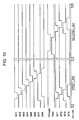
- the driving circuit 32 When the moving-image capturing mode (including the monitoring mode) is set by the mode setting unit 36, the driving circuit 32 generates the timing signals at the timing shown in the timing chart of Fig. 4 or 9. When the still-image capturing mode is set by the mode setting unit 36, the driving circuit 32 generates the timing signals at the timing shown in the timing chart of Fig. 6 or 10. The imaging device 31 is driven and controlled by the generated timing signals.
- the signal processing circuit 34 performs signal processing on an output signal of the imaging device 31, such as correlated double sampling (CDS) and analog-to-digital (A/D) conversion.
- CDS correlated double sampling
- A/D analog-to-digital
- the signal processing circuit 34 rearranges three-line or two-line pixel signals output by the three-line sequence (the first embodiment) or the two-line sequence (the second embodiment) from the imaging device 31 using, for example, a line memory.
- the image recording device 35 records the image signal processed by the signal processing circuit onto a recording medium.
- the image information recorded on the recording medium is hard-copied using a printer or the like.
- the image display device 35 displays the image signal processed by the signal processing circuit 34 on a display monitor such as a liquid crystal display.
- the CCD imaging device 10 allows significant reduction of the occurrence of smearing in the video mode and allows reduction in chip size and cost. A low-cost high-quality imaging apparatus with reduction of the occurrence of smearing can therefore be achieved.
Landscapes
- Engineering & Computer Science (AREA)
- Multimedia (AREA)
- Signal Processing (AREA)
- Transforming Light Signals Into Electric Signals (AREA)
- Solid State Image Pick-Up Elements (AREA)
Applications Claiming Priority (1)
| Application Number | Priority Date | Filing Date | Title |
|---|---|---|---|
| JP2004315490A JP4524609B2 (ja) | 2004-10-29 | 2004-10-29 | 固体撮像素子、固体撮像素子の駆動方法および撮像装置 |
Publications (3)
| Publication Number | Publication Date |
|---|---|
| EP1655952A2 true EP1655952A2 (fr) | 2006-05-10 |
| EP1655952A3 EP1655952A3 (fr) | 2011-09-07 |
| EP1655952B1 EP1655952B1 (fr) | 2012-12-05 |
Family
ID=35589533
Family Applications (1)
| Application Number | Title | Priority Date | Filing Date |
|---|---|---|---|
| EP05023689A Expired - Lifetime EP1655952B1 (fr) | 2004-10-29 | 2005-10-28 | Dispositif de prise d'images à l'état solide, sa méthode de commande et appareil de prise d'images |
Country Status (5)
| Country | Link |
|---|---|
| US (2) | US7616246B2 (fr) |
| EP (1) | EP1655952B1 (fr) |
| JP (1) | JP4524609B2 (fr) |
| KR (1) | KR101182973B1 (fr) |
| TW (1) | TWI280790B (fr) |
Families Citing this family (29)
| Publication number | Priority date | Publication date | Assignee | Title |
|---|---|---|---|---|
| JP2001238134A (ja) * | 2000-02-23 | 2001-08-31 | Sony Corp | 固体撮像素子およびその駆動方法並びにカメラシステム |
| JP4687155B2 (ja) * | 2005-03-09 | 2011-05-25 | ソニー株式会社 | 固体撮像装置およびその駆動方法 |
| JP4457961B2 (ja) * | 2005-04-28 | 2010-04-28 | ソニー株式会社 | 固体撮像素子 |
| JP4639406B2 (ja) * | 2006-03-31 | 2011-02-23 | 富士フイルム株式会社 | 撮像装置 |
| JP4813235B2 (ja) * | 2006-04-05 | 2011-11-09 | パナソニック株式会社 | 固体撮像装置および固体撮像素子の駆動方法 |
| JP4786446B2 (ja) * | 2006-07-19 | 2011-10-05 | パナソニック株式会社 | 固体撮像装置、その駆動方法およびカメラ |
| JP2008104013A (ja) * | 2006-10-19 | 2008-05-01 | Fujifilm Corp | 固体撮像素子の駆動方法及び撮像装置。 |
| JP5084430B2 (ja) * | 2006-11-02 | 2012-11-28 | ペンタックスリコーイメージング株式会社 | 撮像ユニット |
| JP2008193050A (ja) * | 2007-01-12 | 2008-08-21 | Sony Corp | 固体撮像装置および撮像装置 |
| JP2008244738A (ja) * | 2007-03-27 | 2008-10-09 | Fujifilm Corp | 撮像装置および撮像素子の駆動制御方法 |
| JP5163935B2 (ja) * | 2007-05-17 | 2013-03-13 | ソニー株式会社 | イメージセンサ |
| JP2008294913A (ja) * | 2007-05-28 | 2008-12-04 | Panasonic Corp | 固体撮像装置およびその駆動方法 |
| US20100165166A1 (en) * | 2007-06-08 | 2010-07-01 | Panasonic Corporation | Solid-state imaging device |
| US7965331B2 (en) * | 2007-07-23 | 2011-06-21 | Fujifilm Corporation | Solid state imaging element, image pickup device and method of driving solid state imaging element |
| JP4386118B2 (ja) | 2007-08-31 | 2009-12-16 | ソニー株式会社 | 撮像回路 |
| JP2009076746A (ja) * | 2007-09-21 | 2009-04-09 | Fujifilm Corp | 固体撮像素子、撮像装置、及び固体撮像素子の製造方法 |
| US7948534B2 (en) * | 2008-10-22 | 2011-05-24 | Eastman Kodak Company | Charge-coupled device image sensor with vertical binning of same-color pixels |
| JPWO2010103814A1 (ja) * | 2009-03-11 | 2012-09-13 | パナソニック株式会社 | 固体撮像装置 |
| JP2011077914A (ja) | 2009-09-30 | 2011-04-14 | Panasonic Corp | 固体撮像装置及びその駆動方法並びにカメラ |
| JP2011077939A (ja) * | 2009-09-30 | 2011-04-14 | Panasonic Corp | 固体撮像装置及びそれを備えるカメラ |
| JP5640509B2 (ja) * | 2010-07-09 | 2014-12-17 | ソニー株式会社 | 固体撮像素子およびカメラシステム |
| EP2685725B1 (fr) * | 2011-03-11 | 2016-12-07 | FUJIFILM Corporation | Dispositif d'imagerie et programme d'imagerie |
| JP5839998B2 (ja) * | 2012-01-10 | 2016-01-06 | キヤノン株式会社 | 固体撮像装置 |
| JP5573978B2 (ja) * | 2012-02-09 | 2014-08-20 | 株式会社デンソー | 固体撮像素子およびその駆動方法 |
| JP6270423B2 (ja) * | 2013-11-14 | 2018-01-31 | キヤノン株式会社 | 画像処理装置およびその制御方法 |
| US9775113B2 (en) * | 2014-12-11 | 2017-09-26 | Mediatek Inc. | Voice wakeup detecting device with digital microphone and associated method |
| KR102331920B1 (ko) * | 2014-12-26 | 2021-11-29 | 삼성전자주식회사 | 동작 정보, 조도 정보 및 근접 정보를 위한 센서 및 그 센서를 이용하는 프로세서의 동작 방법 |
| WO2017022218A1 (fr) * | 2015-08-04 | 2017-02-09 | パナソニックIpマネジメント株式会社 | Dispositif d'imagerie à semi-conducteurs |
| CN113709372B (zh) * | 2021-08-27 | 2024-01-23 | 维沃移动通信(杭州)有限公司 | 图像生成方法和电子设备 |
Family Cites Families (14)
| Publication number | Priority date | Publication date | Assignee | Title |
|---|---|---|---|---|
| JP3156503B2 (ja) * | 1994-05-27 | 2001-04-16 | 松下電器産業株式会社 | 固体撮像装置の駆動方法及び固体撮像装置の信号処理回路 |
| JPH10136244A (ja) * | 1996-11-01 | 1998-05-22 | Olympus Optical Co Ltd | 電子的撮像装置 |
| US6452634B1 (en) * | 1996-12-26 | 2002-09-17 | Sony Corporation | Charge transfer device and method of driving the same, and solid state imaging device and method of driving the same |
| JP4140077B2 (ja) * | 1998-02-18 | 2008-08-27 | ソニー株式会社 | 固体撮像素子の駆動方法及び固体撮像素子、並びにカメラ |
| JP4178621B2 (ja) * | 1998-10-30 | 2008-11-12 | ソニー株式会社 | 固体撮像素子およびその駆動方法並びにカメラシステム |
| JP4171137B2 (ja) * | 1999-06-08 | 2008-10-22 | 富士フイルム株式会社 | 固体撮像装置及びその制御方法 |
| JP2001111026A (ja) * | 1999-10-07 | 2001-04-20 | Fuji Film Microdevices Co Ltd | 固体撮像装置 |
| JP2001238134A (ja) * | 2000-02-23 | 2001-08-31 | Sony Corp | 固体撮像素子およびその駆動方法並びにカメラシステム |
| JP4514912B2 (ja) * | 2000-07-21 | 2010-07-28 | 富士フイルム株式会社 | 固体撮像装置およびその駆動方法 |
| JP3664123B2 (ja) * | 2001-10-03 | 2005-06-22 | ソニー株式会社 | 撮像装置および画質補正方法 |
| JP3848650B2 (ja) * | 2002-11-12 | 2006-11-22 | 松下電器産業株式会社 | 固体撮像素子およびこれを備えたカメラ |
| JP4658470B2 (ja) * | 2003-11-28 | 2011-03-23 | パナソニック株式会社 | 固体撮像素子、固体撮像装置及びカメラ |
| US20050280726A1 (en) * | 2004-06-18 | 2005-12-22 | Eastman Kodak Company | Image sensor for still or video photography |
| US20060044441A1 (en) * | 2004-08-27 | 2006-03-02 | Eastman Kodak Company | Image sensor for still or video photography |
-
2004
- 2004-10-29 JP JP2004315490A patent/JP4524609B2/ja not_active Expired - Fee Related
-
2005
- 2005-10-24 US US11/256,996 patent/US7616246B2/en not_active Expired - Fee Related
- 2005-10-27 TW TW094137638A patent/TWI280790B/zh not_active IP Right Cessation
- 2005-10-28 KR KR1020050102197A patent/KR101182973B1/ko not_active Expired - Fee Related
- 2005-10-28 EP EP05023689A patent/EP1655952B1/fr not_active Expired - Lifetime
-
2009
- 2009-09-03 US US12/553,276 patent/US7796170B2/en not_active Expired - Fee Related
Also Published As
| Publication number | Publication date |
|---|---|
| EP1655952B1 (fr) | 2012-12-05 |
| US7796170B2 (en) | 2010-09-14 |
| US20090316035A1 (en) | 2009-12-24 |
| JP2006129137A (ja) | 2006-05-18 |
| TWI280790B (en) | 2007-05-01 |
| TW200629889A (en) | 2006-08-16 |
| KR20060052307A (ko) | 2006-05-19 |
| KR101182973B1 (ko) | 2012-09-18 |
| US7616246B2 (en) | 2009-11-10 |
| US20060092304A1 (en) | 2006-05-04 |
| EP1655952A3 (fr) | 2011-09-07 |
| JP4524609B2 (ja) | 2010-08-18 |
Similar Documents
| Publication | Publication Date | Title |
|---|---|---|
| US7796170B2 (en) | Solid-state imaging device with enhanced pixel thinning out configuration and method for driving same | |
| JP2000307961A (ja) | 固体撮像装置およびその駆動方法並びにカメラシステム | |
| US20070258004A1 (en) | Solid-state imaging device, driving method thereof, and camera | |
| US8373780B2 (en) | Solid-state image sensor and camera | |
| JP4814112B2 (ja) | 固体撮像素子 | |
| JP3985275B2 (ja) | 撮像装置および撮像方法 | |
| JP3948042B2 (ja) | カメラシステム、撮像装置および撮像方法 | |
| JP5045183B2 (ja) | 固体撮像素子および固体撮像素子の駆動方法、並びにカメラシステム | |
| JP3664621B2 (ja) | Ccd固体撮像素子の駆動方法 | |
| JP5218342B2 (ja) | 固体撮像素子の駆動方法 | |
| JP2008199419A (ja) | 固体撮像装置、その駆動方法およびカメラ | |
| JP3948456B2 (ja) | 固体撮像素子および固体撮像素子の制御方法 | |
| JP2001119629A (ja) | 固体撮像装置およびその駆動方法 | |
| JP2001145025A (ja) | 固体撮像装置およびその駆動方法 | |
| JPH05268523A (ja) | ビデオカメラ | |
| JP4311473B2 (ja) | 撮像装置 | |
| JP3878775B2 (ja) | 固体撮像装置とこれを用いたカメラおよび固体撮像装置の駆動方法 | |
| JP2010193114A (ja) | 固体撮像装置およびその駆動方法、並びに電子情報機器 | |
| JP2011077732A (ja) | 固体撮像装置およびその駆動方法、並びに電子情報機器 | |
| JP2012235246A (ja) | 固体撮像装置及びその駆動方法と、該固体撮像装置を用いるカメラ | |
| JP2011244173A (ja) | 固体撮像装置及びその駆動方法並びにカメラ | |
| JP2013009266A (ja) | 固体撮像装置及び撮像装置 | |
| JP2009177401A (ja) | Ccd型固体撮像素子の駆動方法及び撮像装置 | |
| JP2011066503A (ja) | 固体撮像装置および固体撮像システム |
Legal Events
| Date | Code | Title | Description |
|---|---|---|---|
| PUAI | Public reference made under article 153(3) epc to a published international application that has entered the european phase |
Free format text: ORIGINAL CODE: 0009012 |
|
| AK | Designated contracting states |
Kind code of ref document: A2 Designated state(s): AT BE BG CH CY CZ DE DK EE ES FI FR GB GR HU IE IS IT LI LT LU LV MC NL PL PT RO SE SI SK TR |
|
| AX | Request for extension of the european patent |
Extension state: AL BA HR MK YU |
|
| REG | Reference to a national code |
Ref country code: DE Ref legal event code: R079 Ref document number: 602005037256 Country of ref document: DE Free format text: PREVIOUS MAIN CLASS: H04N0003150000 Ipc: H04N0005335000 |
|
| PUAL | Search report despatched |
Free format text: ORIGINAL CODE: 0009013 |
|
| AK | Designated contracting states |
Kind code of ref document: A3 Designated state(s): AT BE BG CH CY CZ DE DK EE ES FI FR GB GR HU IE IS IT LI LT LU LV MC NL PL PT RO SE SI SK TR |
|
| AX | Request for extension of the european patent |
Extension state: AL BA HR MK YU |
|
| RIC1 | Information provided on ipc code assigned before grant |
Ipc: H04N 5/335 20110101AFI20110804BHEP |
|
| 17P | Request for examination filed |
Effective date: 20120302 |
|
| AKX | Designation fees paid |
Designated state(s): DE FR GB |
|
| GRAP | Despatch of communication of intention to grant a patent |
Free format text: ORIGINAL CODE: EPIDOSNIGR1 |
|
| GRAS | Grant fee paid |
Free format text: ORIGINAL CODE: EPIDOSNIGR3 |
|
| GRAA | (expected) grant |
Free format text: ORIGINAL CODE: 0009210 |
|
| RAP1 | Party data changed (applicant data changed or rights of an application transferred) |
Owner name: SONY CORPORATION |
|
| RIN1 | Information on inventor provided before grant (corrected) |
Inventor name: HIROTA, ISAO |
|
| AK | Designated contracting states |
Kind code of ref document: B1 Designated state(s): DE FR GB |
|
| REG | Reference to a national code |
Ref country code: GB Ref legal event code: FG4D |
|
| REG | Reference to a national code |
Ref country code: DE Ref legal event code: R096 Ref document number: 602005037256 Country of ref document: DE Effective date: 20130131 |
|
| PLBE | No opposition filed within time limit |
Free format text: ORIGINAL CODE: 0009261 |
|
| STAA | Information on the status of an ep patent application or granted ep patent |
Free format text: STATUS: NO OPPOSITION FILED WITHIN TIME LIMIT |
|
| 26N | No opposition filed |
Effective date: 20130906 |
|
| REG | Reference to a national code |
Ref country code: DE Ref legal event code: R097 Ref document number: 602005037256 Country of ref document: DE Effective date: 20130906 |
|
| PGFP | Annual fee paid to national office [announced via postgrant information from national office to epo] |
Ref country code: DE Payment date: 20141022 Year of fee payment: 10 Ref country code: FR Payment date: 20141022 Year of fee payment: 10 Ref country code: GB Payment date: 20141021 Year of fee payment: 10 |
|
| REG | Reference to a national code |
Ref country code: DE Ref legal event code: R119 Ref document number: 602005037256 Country of ref document: DE |
|
| GBPC | Gb: european patent ceased through non-payment of renewal fee |
Effective date: 20151028 |
|
| PG25 | Lapsed in a contracting state [announced via postgrant information from national office to epo] |
Ref country code: DE Free format text: LAPSE BECAUSE OF NON-PAYMENT OF DUE FEES Effective date: 20160503 Ref country code: GB Free format text: LAPSE BECAUSE OF NON-PAYMENT OF DUE FEES Effective date: 20151028 |
|
| REG | Reference to a national code |
Ref country code: FR Ref legal event code: ST Effective date: 20160630 |
|
| PG25 | Lapsed in a contracting state [announced via postgrant information from national office to epo] |
Ref country code: FR Free format text: LAPSE BECAUSE OF NON-PAYMENT OF DUE FEES Effective date: 20151102 |