EP1657059A2 - Piezoelektrischer Aktor, Verfahren zur Herstellung eines piezoelektrischen Aktors, und Flüssigkeitstransportgerät - Google Patents
Piezoelektrischer Aktor, Verfahren zur Herstellung eines piezoelektrischen Aktors, und Flüssigkeitstransportgerät Download PDFInfo
- Publication number
- EP1657059A2 EP1657059A2 EP05024717A EP05024717A EP1657059A2 EP 1657059 A2 EP1657059 A2 EP 1657059A2 EP 05024717 A EP05024717 A EP 05024717A EP 05024717 A EP05024717 A EP 05024717A EP 1657059 A2 EP1657059 A2 EP 1657059A2
- Authority
- EP
- European Patent Office
- Prior art keywords
- vibration plate
- section
- piezoelectric layer
- supporting member
- bump
- Prior art date
- Legal status (The legal status is an assumption and is not a legal conclusion. Google has not performed a legal analysis and makes no representation as to the accuracy of the status listed.)
- Granted
Links
Images







Classifications
-
- B—PERFORMING OPERATIONS; TRANSPORTING
- B41—PRINTING; LINING MACHINES; TYPEWRITERS; STAMPS
- B41J—TYPEWRITERS; SELECTIVE PRINTING MECHANISMS, i.e. MECHANISMS PRINTING OTHERWISE THAN FROM A FORME; CORRECTION OF TYPOGRAPHICAL ERRORS
- B41J2/00—Typewriters or selective printing mechanisms characterised by the printing or marking process for which they are designed
- B41J2/005—Typewriters or selective printing mechanisms characterised by the printing or marking process for which they are designed characterised by bringing liquid or particles selectively into contact with a printing material
- B41J2/01—Ink jet
- B41J2/135—Nozzles
- B41J2/16—Production of nozzles
- B41J2/1621—Manufacturing processes
- B41J2/1626—Manufacturing processes etching
-
- B—PERFORMING OPERATIONS; TRANSPORTING
- B41—PRINTING; LINING MACHINES; TYPEWRITERS; STAMPS
- B41J—TYPEWRITERS; SELECTIVE PRINTING MECHANISMS, i.e. MECHANISMS PRINTING OTHERWISE THAN FROM A FORME; CORRECTION OF TYPOGRAPHICAL ERRORS
- B41J2/00—Typewriters or selective printing mechanisms characterised by the printing or marking process for which they are designed
- B41J2/005—Typewriters or selective printing mechanisms characterised by the printing or marking process for which they are designed characterised by bringing liquid or particles selectively into contact with a printing material
- B41J2/01—Ink jet
- B41J2/135—Nozzles
- B41J2/14—Structure thereof only for on-demand ink jet heads
- B41J2/14201—Structure of print heads with piezoelectric elements
- B41J2/14233—Structure of print heads with piezoelectric elements of film type, deformed by bending and disposed on a diaphragm
-
- B—PERFORMING OPERATIONS; TRANSPORTING
- B41—PRINTING; LINING MACHINES; TYPEWRITERS; STAMPS
- B41J—TYPEWRITERS; SELECTIVE PRINTING MECHANISMS, i.e. MECHANISMS PRINTING OTHERWISE THAN FROM A FORME; CORRECTION OF TYPOGRAPHICAL ERRORS
- B41J2/00—Typewriters or selective printing mechanisms characterised by the printing or marking process for which they are designed
- B41J2/005—Typewriters or selective printing mechanisms characterised by the printing or marking process for which they are designed characterised by bringing liquid or particles selectively into contact with a printing material
- B41J2/01—Ink jet
- B41J2/135—Nozzles
- B41J2/16—Production of nozzles
- B41J2/1607—Production of print heads with piezoelectric elements
- B41J2/161—Production of print heads with piezoelectric elements of film type, deformed by bending and disposed on a diaphragm
-
- B—PERFORMING OPERATIONS; TRANSPORTING
- B41—PRINTING; LINING MACHINES; TYPEWRITERS; STAMPS
- B41J—TYPEWRITERS; SELECTIVE PRINTING MECHANISMS, i.e. MECHANISMS PRINTING OTHERWISE THAN FROM A FORME; CORRECTION OF TYPOGRAPHICAL ERRORS
- B41J2/00—Typewriters or selective printing mechanisms characterised by the printing or marking process for which they are designed
- B41J2/005—Typewriters or selective printing mechanisms characterised by the printing or marking process for which they are designed characterised by bringing liquid or particles selectively into contact with a printing material
- B41J2/01—Ink jet
- B41J2/135—Nozzles
- B41J2/16—Production of nozzles
- B41J2/1621—Manufacturing processes
- B41J2/1623—Manufacturing processes bonding and adhesion
-
- B—PERFORMING OPERATIONS; TRANSPORTING
- B41—PRINTING; LINING MACHINES; TYPEWRITERS; STAMPS
- B41J—TYPEWRITERS; SELECTIVE PRINTING MECHANISMS, i.e. MECHANISMS PRINTING OTHERWISE THAN FROM A FORME; CORRECTION OF TYPOGRAPHICAL ERRORS
- B41J2/00—Typewriters or selective printing mechanisms characterised by the printing or marking process for which they are designed
- B41J2/005—Typewriters or selective printing mechanisms characterised by the printing or marking process for which they are designed characterised by bringing liquid or particles selectively into contact with a printing material
- B41J2/01—Ink jet
- B41J2/135—Nozzles
- B41J2/16—Production of nozzles
- B41J2/1621—Manufacturing processes
- B41J2/1632—Manufacturing processes machining
- B41J2/1634—Manufacturing processes machining laser machining
-
- B—PERFORMING OPERATIONS; TRANSPORTING
- B41—PRINTING; LINING MACHINES; TYPEWRITERS; STAMPS
- B41J—TYPEWRITERS; SELECTIVE PRINTING MECHANISMS, i.e. MECHANISMS PRINTING OTHERWISE THAN FROM A FORME; CORRECTION OF TYPOGRAPHICAL ERRORS
- B41J2/00—Typewriters or selective printing mechanisms characterised by the printing or marking process for which they are designed
- B41J2/005—Typewriters or selective printing mechanisms characterised by the printing or marking process for which they are designed characterised by bringing liquid or particles selectively into contact with a printing material
- B41J2/01—Ink jet
- B41J2/135—Nozzles
- B41J2/16—Production of nozzles
- B41J2/1621—Manufacturing processes
- B41J2/164—Manufacturing processes thin film formation
- B41J2/1642—Manufacturing processes thin film formation thin film formation by CVD [chemical vapor deposition]
-
- B—PERFORMING OPERATIONS; TRANSPORTING
- B41—PRINTING; LINING MACHINES; TYPEWRITERS; STAMPS
- B41J—TYPEWRITERS; SELECTIVE PRINTING MECHANISMS, i.e. MECHANISMS PRINTING OTHERWISE THAN FROM A FORME; CORRECTION OF TYPOGRAPHICAL ERRORS
- B41J2/00—Typewriters or selective printing mechanisms characterised by the printing or marking process for which they are designed
- B41J2/005—Typewriters or selective printing mechanisms characterised by the printing or marking process for which they are designed characterised by bringing liquid or particles selectively into contact with a printing material
- B41J2/01—Ink jet
- B41J2/135—Nozzles
- B41J2/16—Production of nozzles
- B41J2/1621—Manufacturing processes
- B41J2/164—Manufacturing processes thin film formation
- B41J2/1646—Manufacturing processes thin film formation thin film formation by sputtering
-
- H—ELECTRICITY
- H05—ELECTRIC TECHNIQUES NOT OTHERWISE PROVIDED FOR
- H05K—PRINTED CIRCUITS; CASINGS OR CONSTRUCTIONAL DETAILS OF ELECTRIC APPARATUS; MANUFACTURE OF ASSEMBLAGES OF ELECTRICAL COMPONENTS
- H05K3/00—Apparatus or processes for manufacturing printed circuits
- H05K3/36—Assembling printed circuits with other printed circuits
- H05K3/361—Assembling flexible printed circuits with other printed circuits
- H05K3/363—Assembling flexible printed circuits with other printed circuits by soldering
-
- H—ELECTRICITY
- H10—SEMICONDUCTOR DEVICES; ELECTRIC SOLID-STATE DEVICES NOT OTHERWISE PROVIDED FOR
- H10N—ELECTRIC SOLID-STATE DEVICES NOT OTHERWISE PROVIDED FOR
- H10N30/00—Piezoelectric or electrostrictive devices
- H10N30/20—Piezoelectric or electrostrictive devices with electrical input and mechanical output, e.g. functioning as actuators or vibrators
- H10N30/204—Piezoelectric or electrostrictive devices with electrical input and mechanical output, e.g. functioning as actuators or vibrators using bending displacement, e.g. unimorph, bimorph or multimorph cantilever or membrane benders
- H10N30/2047—Membrane type
-
- B—PERFORMING OPERATIONS; TRANSPORTING
- B41—PRINTING; LINING MACHINES; TYPEWRITERS; STAMPS
- B41J—TYPEWRITERS; SELECTIVE PRINTING MECHANISMS, i.e. MECHANISMS PRINTING OTHERWISE THAN FROM A FORME; CORRECTION OF TYPOGRAPHICAL ERRORS
- B41J2/00—Typewriters or selective printing mechanisms characterised by the printing or marking process for which they are designed
- B41J2/005—Typewriters or selective printing mechanisms characterised by the printing or marking process for which they are designed characterised by bringing liquid or particles selectively into contact with a printing material
- B41J2/01—Ink jet
- B41J2/135—Nozzles
- B41J2/14—Structure thereof only for on-demand ink jet heads
- B41J2/14201—Structure of print heads with piezoelectric elements
- B41J2/14233—Structure of print heads with piezoelectric elements of film type, deformed by bending and disposed on a diaphragm
- B41J2002/14266—Sheet-like thin film type piezoelectric element
-
- B—PERFORMING OPERATIONS; TRANSPORTING
- B41—PRINTING; LINING MACHINES; TYPEWRITERS; STAMPS
- B41J—TYPEWRITERS; SELECTIVE PRINTING MECHANISMS, i.e. MECHANISMS PRINTING OTHERWISE THAN FROM A FORME; CORRECTION OF TYPOGRAPHICAL ERRORS
- B41J2/00—Typewriters or selective printing mechanisms characterised by the printing or marking process for which they are designed
- B41J2/005—Typewriters or selective printing mechanisms characterised by the printing or marking process for which they are designed characterised by bringing liquid or particles selectively into contact with a printing material
- B41J2/01—Ink jet
- B41J2/135—Nozzles
- B41J2/14—Structure thereof only for on-demand ink jet heads
- B41J2002/14491—Electrical connection
-
- H—ELECTRICITY
- H05—ELECTRIC TECHNIQUES NOT OTHERWISE PROVIDED FOR
- H05K—PRINTED CIRCUITS; CASINGS OR CONSTRUCTIONAL DETAILS OF ELECTRIC APPARATUS; MANUFACTURE OF ASSEMBLAGES OF ELECTRICAL COMPONENTS
- H05K2201/00—Indexing scheme relating to printed circuits covered by H05K1/00
- H05K2201/03—Conductive materials
- H05K2201/0332—Structure of the conductor
- H05K2201/0364—Conductor shape
- H05K2201/0367—Metallic bump or raised conductor not used as solder bump
-
- H—ELECTRICITY
- H05—ELECTRIC TECHNIQUES NOT OTHERWISE PROVIDED FOR
- H05K—PRINTED CIRCUITS; CASINGS OR CONSTRUCTIONAL DETAILS OF ELECTRIC APPARATUS; MANUFACTURE OF ASSEMBLAGES OF ELECTRICAL COMPONENTS
- H05K2201/00—Indexing scheme relating to printed circuits covered by H05K1/00
- H05K2201/09—Shape and layout
- H05K2201/09009—Substrate related
- H05K2201/09036—Recesses or grooves in insulating substrate
-
- H—ELECTRICITY
- H05—ELECTRIC TECHNIQUES NOT OTHERWISE PROVIDED FOR
- H05K—PRINTED CIRCUITS; CASINGS OR CONSTRUCTIONAL DETAILS OF ELECTRIC APPARATUS; MANUFACTURE OF ASSEMBLAGES OF ELECTRICAL COMPONENTS
- H05K3/00—Apparatus or processes for manufacturing printed circuits
- H05K3/0058—Laminating printed circuit boards onto other substrates, e.g. metallic substrates
-
- Y—GENERAL TAGGING OF NEW TECHNOLOGICAL DEVELOPMENTS; GENERAL TAGGING OF CROSS-SECTIONAL TECHNOLOGIES SPANNING OVER SEVERAL SECTIONS OF THE IPC; TECHNICAL SUBJECTS COVERED BY FORMER USPC CROSS-REFERENCE ART COLLECTIONS [XRACs] AND DIGESTS
- Y10—TECHNICAL SUBJECTS COVERED BY FORMER USPC
- Y10T—TECHNICAL SUBJECTS COVERED BY FORMER US CLASSIFICATION
- Y10T29/00—Metal working
- Y10T29/42—Piezoelectric device making
Definitions
- the present invention relates to a piezoelectric actuator, a method for manufacturing piezoelectric actuator, and a liquid transporting apparatus which includes the piezoelectric actuator.
- a piezoelectric actuator which drives an object by using a deformation developed in a piezoelectric layer when an electric field is made to act in the piezoelectric actuator has been hitherto used widely in various fields.
- an ink-jet head which discharges ink when a pressure is applied to the ink in a pressure chamber by the piezoelectric actuator, is described in U.S. Patent Application Publication No. US 2003/112298 A1 (corresponding to Japanese Patent Application Laid-open No. 2003-69103).
- This ink-jet head includes a metallic substrate, a plurality of piezoelectric elements (piezoelectric layer) arranged in the form of a matrix on the substrate, a piezoelectric actuator which has common electrodes and signal electrodes (individual electrodes) formed on an upper surface and a lower surface of the piezoelectric elements respectively, and a flexible printed circuit board (FPC) made of a resin base material.
- piezoelectric elements piezoelectric layer
- FPC flexible printed circuit board
- a plurality of terminal sections is formed on the FPC on a surface facing the piezoelectric elements, and these terminal sections correspond to the signal electrodes on the upper surface of the piezoelectric elements.
- Each of the terminal sections has a hemispherical bump which includes a core material and a joining material.
- An object of the present invention is to prevent the damage of a piezoelectric layer by alleviating the concentrated action of the stress locally on the piezoelectric layer while joining the electrodes on the upper surface of the piezoelectric layer and the terminal sections of a wire member such as an FPC, and to prevent the poor connection between the electrodes on the upper surface of the piezoelectric layer and the terminal section of the wire member due to the uneven height of the bumps.
- a piezoelectric actuator which includes a vibration plate (60, 74); a supporting member (40) having a relieving section (pressure chamber) which relieves a deformation of the vibration plate (60, 74), and a joining section (40a) joined to the vibration plate; a first electrode (60, 112) arranged on a surface of the vibration plate on a side opposite to the supporting member (40); a piezoelectric layer (61) which is arranged on a surface of the first electrode on a side opposite to the vibration plate; a second electrode (62) arranged on a surface of the piezoelectric layer on a side opposite to the vibration plate, in an area facing the relieving section; a contact section (62a) formed on the surface of the pie
- an electroconductive bump (65a) is formed on one of a terminal section of the wire member and the contact section, the bump being projected toward the other of the terminal section and the contact section to electrically connect the contact section and the terminal section; and a reduced-stiffness section (60a, 70a, 71a, 73, 75, 76, 78, and 79a) is provided between the vibration plate and the supporting member, or between the vibration plate and the piezoelectric layer, at a portion facing the bump, the reduced-stiffness section having a stiffness reduced than a stiffness of a portion other than the portion facing the bump.
- the concentration of the stress acting on the piezoelectric layer while joining the piezoelectric layer and the wire member is alleviated or relieved by the reduced-stiffness section, and the damage of the piezoelectric layer can be prevented.
- the stiffness is reduced in the area facing the bump, between the vibration plate and the supporting member or between the vibration plate and the piezoelectric layer, the bump and the contact section or the terminal section are adhered more tightly, and the poor connection between the contact section of the second electrode and the terminal section of the wire member due to the uneven height among the bumps can be prevented.
- a portion facing the bump means a portion (area) which includes a position (a position in a direction of a plane of the vibration plate) right below the bump. Accordingly, a case in which no reduced-stiffness section is provided at the position right below the bump does not mean that "a reduced-stiffness section is provided at a portion facing the bump”.
- the reduced-stiffness section of the piezoelectric actuator according to the present invention may be interposed between the vibration plate and the supporting member, and may be a low-elasticity material having a lower elasticity (a lower coef ficient of elasticity) than an elasticity of the vibration plate and an elasticity of the supporting member. Accordingly, the concentration of the stress acting on the piezoelectric layer while joining the piezoelectric layer and the wire member, can be relieved by the reduced-stiffness section, thereby preventing the damage of the piezoelectric layer. In addition, the poor connection between the contact section of the individual electrode and the terminal section of the wire member due to the uneven height of the bumps can be prevented.
- the reduced-stiffness section of the piezoelectric actuator of the present invention may be a through hole or a recess formed in at least one of the vibration plate and the supporting member, at a portion facing the bump, the recess or the through hole being open toward the other of the vibration plate and the supporting member. Accordingly, the concentration of the stress acting on the piezoelectric layer while joining the piezoelectric layer and the wire member can be relieved by the aid of the recess or the hole, thereby preventing the damage of the piezoelectric layer. In addition, the poor connection between the contact section of the individual electrode and the terminal section of the wire member due to the uneven height of the bumps can be prevented.
- a low-elasticity material having a lower elasticity than an elasticity of the vibration plate and an elasticity of the supporting member may be filled in the recess or the hole formed in the vibration plate or the supporting member. Accordingly, the concentration of the stress acting on the piezoelectric layer while joining the piezoelectric layer and the wire member is relieved by the low-elasticity material filled in the recess or the hole, thereby preventing the damage of the piezoelectric layer. In addition, the poor connection between the contact section of the individual electrode and the terminal section of the wire member due to the uneven height of the bumps can be prevented.
- the supporting member of the piezoelectric actuator of the present invention may be formed of a metallic material. Accordingly, the relieving section can be formed easily by a method such as etching. Moreover, when the recess or the hole is formed as the reduced-stiffness section, the recess or the hole can be formed easily. Or, the supporting member may be formed by an insulating material or an adhesive.
- the vibration plate of the piezoelectric actuator of the present invention is made of a metallic material and that the vibration plate serves as the first electrode. Accordingly, a process for separately forming the first electrode is not required and the manufacturing process can be simplified.
- an insulating layer may be interposed between the vibration plate and the piezoelectric layer, and at the portion facing the bump. Accordingly, in the area where the bump is formed, an electrostatic capacitance developed in the piezoelectric layer which is sandwiched between the contact section of the second electrode and the first electrode can be reduced to be smaller and a drive efficiency of the actuator can be improved.
- the insulating layer is formed of a material which has a lower elasticity than an elasticity of the vibration plate and an elasticity of the piezoelectric layer. Accordingly, the concentration of the stress acting on the piezoelectric layer while joining the contact section and the wire member is relieved by the insulating layer, thereby preventing the damage to the piezoelectric layer. In addition, the poor connection between the contact section of the individual electrode and the terminal section of the FPC due to the uneven height of the bumps can be prevented.
- a length of the reduced-stiffness section in a direction of a plane of the piezoelectric layer may be not less than four times of a sum of a thickness of the vibration plate and a thickness of the piezoelectric layer, and particularly about six times or not less than six times of the sum of the thickness of the vibration plate and the thickness of the piezoelectric layer.
- a liquid transporting apparatus which includes a liquid channel having a nozzle, a pressure chamber communicating with the nozzle, and the piezoelectric actuator of the present invention, wherein the relieving section of the supporting member of the piezoelectric actuator corresponds to the pressure chamber.
- the reduced-stiffness section may be a recess or a through hole formed in at least one of the vibration plate and the supporting member, at a portion facing the bump, the recess or the through hole being open toward other of the vibration plate and the supporting member. Accordingly, the concentration of the stress acting on the piezoelectric layer when the wire member is pressed against the contact section, is relieved by the recess or the through hole formed in at least one of the vibration plate and the support member, thereby preventing the damage of the piezoelectric layer. In addition, the poor connection between the individual electrodes and the wire member due to the uneven height of the bumps can be prevented. Therefore, the reliability of the liquid transporting apparatus is improved.
- the pressure chamber may include a plurality of chambers; and the recess or the through hole may be extended at least up to a space between a chamber of the chambers and an adjacent chamber to the chamber. Accordingly, a phenomenon (so called cross-talk), in which the deformation of the piezoelectric layer in an area facing a certain chamber is propagated to another chamber, can be suppressed by the recess.
- the liquid transporting apparatus of the present invention may be applicable to an ink-jet printer.
- a method for manufacturing a piezoelectric actuator including: a first step of providing a reduced-stiffness section between the vibration plate and the supporting member, and at a portion facing a portion in which the bump is to be arranged, the reduced-stiffness section having a stiffness reduced than a stiffness of a portion other than the portion facing the bump; a second step of joining the vibration plate and the supporting member at the joining section; a third step of forming the piezoelectric layer on the surface of the vibration plate on the side opposite to the supporting member, the first electrode being arranged on the surface; a fourth step of forming, on the surface of the piezoelectric layer on the side opposite to the vibration plate, the second electrode in an area facing the relieving section, and a contact section connected to the second electrode in an area facing the joining section; a fifth step of forming the bump having electroconductivity on one of the terminal section of the wire member and the contact section, the bump projecting toward the other
- the concentration of the stress acting on the piezoelectric layer is relieved by the reduced-stiffness section, and the damage of the piezoelectric layer can be prevented.
- the poor connection between the contact section and the terminal section of the wire member due to the uneven height of the bumps can be prevented. Accordingly, it is possible to manufacture a highly reliable piezoelectric actuator.
- a recess or a through hole is formed as the reduced-stiffness section, in at least one of the vibration plate and the supporting member, at a portion facing the portion where the bump is to be arranged, the recess or the hole being open toward the other of the vibration plate and the supporting member. Accordingly, the concentration of the stress acting on the piezoelectric layer can be relieved by the section having the stiffness reduced by being provided with the recess or the hole. In addition, the poor connection between the contact section and the terminal section of the wire member can be prevented. Accordingly, it is possible to manufacture a highly reliable piezoelectric actuator.
- the piezoelectric layer may be formed by an aerosol depos itionmethod or a sputtering method. Accordingly, a thin piezoelectric layer can be formed easily.
- a liquid transporting apparatus which includes a liquid channel (31) including a plurality of pressure chambers (44) arranged along a plane and communicating with nozzles respectively, and a piezoelectric actuator (32) which changes a volume of the pressure chambers to apply pressure to the liquid in the pressure chambers, wherein the piezoelectric actuator includes: a pressure chamber plate (40) in which the pressure chambers are formed; a vibration plate (60) which is joined to one surface of the pressure chamber plate and which covers the plurality of pressure chambers; a common electrode (60, 112) which is arranged on a surface of the vibration plate (60) on a side opposite to the pressure chambers; a piezoelectric layer (61) formed on a surface of the common electrode on a side opposite to the vibration plate; a plurality of individual electrodes (62) which are arranged on a surface of the piezoelectric layer on a side opposite to the vibration plate, in an area facing the pressure chambers respectively; a plurality of contact
- a plurality of electroconductive bumps are formed on one of the wire member and the respective contact sections, the bumps being projected toward the other of the wire member and the contact sections to electrically connect the wire member and the contact sections; and a plurality of reduced-stiffness sections (60a, 70a, 71a, 73, 75, 76, 78, and 79a) are formed on at least one of the vibration plate and the pressure chamber plate, at a portion facing the bumps, each of the reduced-stiffness sections having a stiffness reduced than a stiffness of a portion other than the portion facing the bumps.
- the concentration of the stress acting on the piezoelectric layer is relieved by the reduced-stiffness sections, and the damage of the piezoelectric layer can be prevented. Also, the poor connection between the individual electrodes and the wire member due to the uneven height of the bumps can be prevented. Therefore, the reliability of the liquid transporting apparatus is improved.
- each of the reduced-stiffness sections may be a recess or a through hole formed in at least one of the vibration plate and the pressure chamber plate, at a portion facing one of the bumps, the recess or the through hole being open toward the other of the vibration plate and the pressure chamber plate. Accordingly, the concentration of the stress acting on the piezoelectric layer when the wire member is pressed against the contact section, is relieved by the recess or the through hole formed in at least one of the vibration plate and the pressure chamber plate, thereby preventing the damage of the piezoelectric layer. In addition, the poor connection between the individual electrodes and the wire member due to the uneven height of the bumps can be prevented. Therefore, the reliability of the liquid transporting apparatus is improved.
- the recess or the hole is extended at least up to a space between a pressure chamber of the pressure chambers and an adjacent pressure chamber to the pressure chamber. Accordingly, a phenomenon (so called cross-talk), in which the deformation of the piezoelectric layer in an area facing a certain pressure chamber is propagated to another pressure chamber, can be suppressed by the recess.
- the liquid transporting apparatus of the present invention may be applicable to an ink-jet printer.
- Fig. 1 is a schematic perspective view of an ink-jet printer 1 according to the present invention
- the ink-jet printer 1 which includes an ink-jet head 3 will be described briefly.
- the ink-jet printer 1 includes a carriage 2 movable in a left and right direction in the drawing, an ink-jet head 3 (liquid transporting apparatus) of serial type which is provided on the carriage 2 and discharges ink onto a recording paper P, and transporting rollers 4 which carry the recording paper in a forward direction in Fig. 1.
- the ink-jet head 3 moves integrally with the carriage 2 in a left and right direction (scanning direction) and discharges ink onto the recording paper P from ejecting ports of nozzles 50 (refer to Fig. 2 and Fig. 3) formed in an ink-discharge surface of a lower surface of the ink-jet head 3.
- the recording paper P with an image recorded thereon by the ink-jet head 3 is discharged forward (paper feeding direction) by the transporting rollers 4.
- Fig. 2 is a partially enlarged view of the ink-jet head 3 in Fig. 1 and Fig. 3 is a cross-sectional view of Fig. 2 taken along a line III-III.
- the ink-jet head 3 includes a channel unit 31 in which an ink channel is formed, and a piezoelectric actuator 32 which is arranged on an upper surface of the channel unit 31.
- the channel unit 31 includes a cavity plate 40, a base plate 41, a manifold plate 42, and a nozzle plate 43, and these four plates are joined in stacked layers.
- the cavity plate 40, the base plate 41, and the manifold plate 42 are substantially rectangular stainless steel plates.
- the nozzle plate 43 is formed of a high-molecular synthetic resin material such as polyimide and is joined to a lower surface of the manifold plate 42.
- the nozzle plate 43 may also be formed of a metallic material such as stainless steel similar to the three plates 40 to 42.
- a plurality of pressure chambers 44 arranged along a plane is formed in the cavity plate 40 (pressure chamber plate).
- a part of the plurality of pressure chambers 44 (10 pressure chambers) is shown in Fig. 2.
- Each pressure chamber 44 is substantially elliptical in a plan view and is arranged such that a long axis direction of the pressure chamber is the scanning direction (left and right direction in Fig. 2).
- Communicating holes 45 and 46 are formed in the base plate 41 at positions which overlap, in a plan view, with both end portions of the associated pressure chamber 44 in the long axis direction of the pressure chamber.
- a manifold 47 is formed in the manifold plate 42.
- the manifold 47 is extended in two rows in the paper feeding direction (vertical direction in Fig. 2) and overlaps, in a plan view, with a left end portion or a right end portion of each of the pressure chambers 44 in Fig. 2.
- Ink is supplied to the manifold 47 from an ink tank (not shown in the diagram) via an ink supply port 48 formed in the cavity plate 40.
- a communicating hole 49 is formed at a position overlapping in a plan view with an end portion of each of the pressure chambers 44 on the side opposite to the manifold 47.
- a plurality of nozzles 50 is formed in the nozzle plate 43 at positions each overlapping in a plan view with an end portion of each of the pressure chambers 44 on the side opposite to the manifold.
- the nozzles 50 are formed, by an excimer laser process on a substrate of a high-molecular synthetic resin such as polyimide.
- the manifold 47 communicates with the pressure chamber 44 via the communicating hole 45, and the pressure chamber communicates with the nozzle 50 via the communicating holes 46 and 49.
- a plurality of individual ink channels (liquid channels) from the manifold 47 up to the nozzles 50 via the pressure chambers 44 is formed in the channel unit 31.
- the piezoelectric actuator 32 includes a vibration plate 60, a piezoelectric layer 61, a plurality of individual electrodes 62, and a flexible printed circuit board (FPC) 65.
- the vibration plate 60 which is electroconductive is arranged on a surface of the cavity plate 40 and joined to the cavity plate 40.
- the piezoelectric layer 61 is formed continuously on a surface of the vibration plate 60, spreading across the pressure chambers 44.
- the individual electrodes 62 are formed on the surface of the piezoelectric layer 61 corresponding to the respective pressure chambers 44.
- the flexible printed circuit board (FPC) 65 is provided over the individual electrodes.
- the cavity plate 40 (supporting member) of the channel unit 31 also constructs a part of the piezoelectric actuator 32.
- This cavity plate 40 has a joining section 40a joined to the vibration plate 60 and the pressure chamber 44 as a reliving section for relieving a deformation of the vibration plate 60.
- the vibration plate 60 is made of a metallic material such as an iron alloy like stainless steel, a nickel alloy, an aluminum alloy, and a titanium alloy.
- the vibration plate 60 is joined to the joining section 40a of the cavity plate 40 such that the vibration plate 60 covers the plurality of pressure chambers 44.
- This vibration plate 60 faces the plurality of individual electrodes 62 and serves also as a common electrode which generates an electric field in the piezoelectric layer 61 between the individual electrodes 62 and the vibration plate 60.
- the vibration plate 60 is grounded and is kept at a ground potential. Moreover, as shown in Fig.
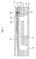
- a recess 60a having a circular shape is formed in an area of the vibration plate 60 on a side of the cavity plate 40, the area being included, in a plan view, in the joining section 40a of the cavity plate 40.
- the recess 60a is formed in the vibration plate 60 by a method such as half etching.
- the piezoelectric layer 61 which is composed of mainly lead zirconate titanate (PZT) which is a solid solution of lead titanate and lead zirconate, and is a ferroelectric substance, is formed on the surface of the vibration plate 60.
- the piezoelectric layer 61 is formed spreading across the pressure chambers 44. Therefore the piezoelectric layer 61 can be formed at one time for all the pressure chambers 44, thereby making the formation of the piezoelectric layer 61 easy.
- the piezoelectric layer 61 can be formed for example, by an aerosol deposition method (AD method) in which ultra fine particles of a piezoelectric material are deposited by causing the particles to collide at a high speed on the surface of the vibration plate 60.
- AD method aerosol deposition method
- a method such as a sol-gel method, a sputtering method, a hydrothermal synthesis method, or a CVD (chemical vapor deposition) method can also be used to form the piezoelectric layer 61.
- the piezoelectric layer 61 can also be formed by sticking a piezoelectric sheet, obtained by baking a green sheet of PZT, on the surface of the vibration plate 60.
- the individual electrodes 62 On the upper surface of the piezoelectric layer 61, the individual electrodes 62 having flat shape and substantially elliptical form and a size smaller than the size of the pressure chamber 44 to some extent are formed. Each of these individual electrodes 62 is formed to overlap with a central portion of the corresponding pressure chamber 44 in a plan view.
- the individual electrodes 62 are made of an electroconductive material such as gold, copper, silver, palladium, platinum, and titanium.
- a plurality of contact sections 62a are formed on the upper surface of the piezoelectric layer 61.
- Each of the contact sections 62a extends from one end portion (an end portion on the side of the manifold 47) of one of the individual electrodes 62 up to a portion facing the recess 60a which is positioned in the joining section 40a in plan view.
- the individual electrodes 62 and the contact sections 62a can be formed by a method such as screen printing, a sputtering method, and a vapor deposition method.
- the FPC 65 includes terminal sections 65a corresponding to the contact sections 62a in the lower surface side of a substrate made of a material such as polyimide. On surfaces of these terminal sections 65a, a plurality of hemispherical bumps 66 made of solder and projecting toward the contact sections 62a are respectively formed. The contact sections 62a and the terminal sections 65a are electrically connected via the bumps 66.
- the bump 66 is included, in a plan view, completely inside the circular shaped recess 60a. In other words, a part of the recess 60a is right below the bump 66.
- the FPC 65 is connected to a driver IC (not shown in the diagram) which supplies a drive signal.
- the contact sections 62a and the terminal sections 65a are connected by allowing the plurality of bumps 66 formed on the plurality of terminal sections 65a respectively to make a contact with the contact sections 62a of the plurality of individual electrodes 62, and by pressing the FPC 65 toward the individual electrodes 62 while heating the FPC 65 by a ceramic heater (not shown in the diagram) from a surface of the FPC 65 on a side opposite to the individual electrodes 62.
- the recess 62a is formed on the vibration plate 60 in an area facing the bump 66, thereby reducing the stiffness partially (reducing the area of the vibration plate in which the recess is formed). Therefore, the concentration of the stress acting on the piezoelectric layer 61 when the FPC 65 is pressed is relieved. This will be described later in further detail.
- the vibration plate 60 and the piezoelectric layer 61 in the area facing a pressure chamber 44 are deformed so as to project toward the pressure chamber 44. Accordingly, avolumeofthepressurechamber 44 is decreased and there is a rise in an ink pressure. Therefore, the ink is discharged from the nozzle 50 communicating with the pressure chamber 44.
- Fig. 4 is a diagram showing a manufacturing process of the ink-jet head 3.
- the recesses 60a are formed by half etching on a surface of the vibration plate 60 made of a metallic material on a side where the vibration plate 60 is joined to the cavity plate 40 (first step).
- the vibration plate 60, the cavity plate 40, the base plate 41, and the manifold plate 42 are joined (second step).
- the plates are joined by metal diffusion joining. Or the plates may be joined with an adhesive.
- at least the vibration plate 60 and the cavity plate 40 may be joined, and the base plate 41 and the manifold plate 42 may be joined later.
- the PZT is formed on the surface of the vibration plate on the side opposite to the cavity plate 40 by a method such as the aerosol deposition method (AD method), the sol-gel method, the sputtering method, the hydrothermal synthesis method, or the CVD (chemical vapor deposition) method, thereby forming the piezoelectric layer 61 (third step).
- a method such as the AD method, the sol-gel method, the sputtering method, the hydrothermal synthesis method, or the CVD method
- a thin piezoelectric layer 61 can be formed easily and the manufacturing process can be simplified.
- the piezoelectric layer 61 may also be formed by sticking, on the surface of the vibration plate 60, the piezoelectric sheet obtained by baking the green sheet of PZT.
- the individual electrodes 62 are formed on a surface of the piezoelectric layer 61 on a side opposite to the vibration plate, in an area of this surface facing the pressure chambers 44, and the contact sections 62a are formed in an area facing the joining sections 40a and in an area facing the recesses 60a (fourth step).
- the bumps 66 projecting toward the individual electrodes 62 are formed by soldering or the like on the terminal sections 6 5a of the FPC 65 (fifth step). Further, the contact sections 62a and the bumps 66 are positioned to make a contact with each other, and the contact sections 62a of the individual electrodes 62 and the terminal sections 65a of the wire member 65 are electrically connected via the bumps 66 by pressing the FPC 65 toward the individual electrodes 62 while heating the FPC 65 by a ceramic heater from the surface of the FPC 65 on the side opposite to the individual electrodes 62 (sixth step).
- the recesses 60a are provided in the area facing the bumps 66, while joining the contact sections 62a and the bumps 66, a stress acts on the piezoelectric layer 61 due to pressing the FPC by using the ceramic heater or the like toward the individual electrodes 62, and in the area facing the recesses 60a, the vibration plate 60 and the piezoelectric layer 61 are bent toward the recesses 60a. Accordingly, the concentration of the stress in the piezoelectric layer 61 in the area facing the bumps 66 is relieved and the damage of the piezoelectric layer 61 can be prevented.
- the bumps 66 having greater height come in contact with the contact sections 62a.
- the contact sections 62a corresponding to the bumps having the greater height are pressed by the bumps having greater height, and the vibration plate 60 and the piezoelectric layer 61 in an area facing the portion in which these bumps 66 and the contact sections 62a are in contact is bent toward the recesses 60a, and as a result, the bumps 66 having a smaller height also come in contact with the contact sections 62a. Accordingly, an adhesion between the bumps 66 and the contact sections 62a is improved, and any poor contact between the contact sections 62a and the terminal section 65a can be prevented.
- the nozzle plate 43 is joined with an adhesive or the like to a lower surface of the manifold plate 42 (seventh step).
- the ink-jet head 3 is manufactured.
- the nozzle plate 43 is made of a metallic material, in the second step, the nozzle plate 43 may be joined at the same time.
- the vibration plate 60 When the thickness of the vibration plate 60 is made to be 20 ⁇ m, the diameter of the circular recesses 60a is made to be 180 ⁇ m, the depth of the circular recesses 60a is made to be 10 ⁇ m, the thickness of the piezoelectric layer 61 is made to be 10 ⁇ m, and the pressing weight of the bumps 66 is made to be 30 g, in the area where the recesses 60a are formed, the vibration plate 60 can be deformed by about 2 ⁇ m, and even if there is an unevenness in height of the bumps 66 of about 2 ⁇ m, the contact sections 62a and the terminal sections 65a can be joined stably.
- a size (diameter) of the recess 60a is not less than four times of a sum of thicknesses of the vibration plate 60 and the piezoelectric layer 61.
- the size of the recess 60a is not less than six times of the sum of the thicknesses of the vibration plate 60 and the piezoelectric layer 61.
- the recess 60a is circular in shape.
- the recess may have any shape such as a rectangular shape or a polygonal shape, and even in such case the size (length) mentioned above is desirable.
- a low-elasticity material 69 such as a synthetic resin material, having a lower elasticity than an elasticity of the vibration plate 60 and an elasticity of the cavity plate 40, may be filled in the recess 60a formed in the vibration plate 60.
- This low-elasticity material 69 is filled in the recess 60a while performing the second step.
- the concentration of stress on the piezoelectric layer 61 can be relieved by the low-elasticity material 69, and the unevenness in height of the bumps 60 can be absorbed. Accordingly, it is possible to prevent any poor connection between the contact sections 62a and the terminal sections 65a.
- a through hole 70a may be formed in a vibration plate 70 in the area facing the bump 66.
- the piezoelectric layer 61 is formed by sticking, on the vibration plate 70, the piezoelectric sheet made from the baked green sheet.
- the hole 70a is formed, for example, by performing full etching on the vibration plate 70. Even in this case, similarly as in the embodiment described above, the concentration of stress on the piezoelectric layer 61 can be relieved by the hole 70a, and the unevenness in height of the bumps 66 can be absorbed. Accordingly, it is possible to prevent any poor connection between the contact sections 62a and the terminal sections 65a.
- a recess 71a may be formed in a surface of a cavity plate 71 on a side of a vibration plate 74.
- the concentration of stress on the piezoelectric layer 61 can be relieved by the recess 71a, and the unevenness in height of the bumps 66 can be absorbed. Accordingly, it is possible to prevent any poor connection between the contact sections 62a and the terminal sections 65a.
- a through hole 72a is formed in a cavity plate (supporting member) 72 in an area facing the bump 66, an effect similar to the effect in the third modified embodiment can be achieved.
- a low elasticity material having a coefficient of elasticity smaller than a coefficient of elasticity of the vibration plate 74 and the coefficient of elasticity of the the piezoelectric layer 61 may be filled in the recess 71a of the third modified embodiment and the hole 72a of the fourth modified embodiment.
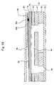
- an insulating layer 73 may be interposed in an area between the piezoelectric layer 61 and the vibration plate 60, the area covering the recess 60a in a plan view.
- the insulating layer 73 is formed by a method such as screen printing between the second step and the third step. In this case, an electrostatic capacitance of the piezoelectric layer 61 sandwiched between the vibration plate 60 and the individual electrodes 62, in an area facing the insulating layer 73, is decreased, and the drive efficiency of the piezoelectric actuator is improved.
- the insulating layer 73 is made of a material having a coefficient of elasticity smaller than the coefficient of elasticity of the piezoelectric layer 61 and the coefficient of elasticity of the vibration plate 60, the effect of relieving of the concentration of stress in the piezoelectric layer 61 and the effect of prevention of any poor connection between the contact sections 62a and the terminal sections 65a, are further improved.
- no recess or no hole may be formed in the vibration plate 74 and the cavity plate 40, but only a low-elasticity material 75 having a coefficient of elasticity smaller than the coefficient of elasticity of the vibration plate 74 and the coefficient of elasticity of the cavity plate 40 may be interposed between the vibration plate 74 and the cavity plate 40.
- the low-elasticity material 75 is formed before the second step by a method such as screen printing on a surface of the cavity plate 40 on the side of the vibration plate 60. Even in this case, similarly as in the embodiment described above, the concentration of stress on the piezoelectric layer 61 can be relieved by the low-elasticity material 75, and the unevenness in height of the bumps 66 can be absorbed.
- the low-elasticity material 75 is formed on the cavity plate 41 in an area corresponding to the joining section 40a. However, the low-elasticity material 75 may be formed at least in the area facing the bump 66.
- no recess or no hole may be formed in the vibration plate 74 and the cavity plate 40, but only a low elasticity material 76 having a coefficient of elasticity smaller than the coefficient of elasticity of the vibration plate 74 and the coefficient of elasticity of the piezoelectric layer 61 may be interposed in a narrow area (diameter of, for example, four to six times of a sum of the thickness of the vibration plate 74 and the thickness of the piezoelectric layer 61), the narrow area being between the vibration plate 74 and the piezoelectric layer 61 and facing the bump 66.
- the low-elasticity material 76 is formed before the third step by a method such as screen printing on the surface of the vibration plate 74 on the side of the piezoelectric layer 61.
- the concentration of stress on the piezoelectric layer 61 can be relieved by the low-elasticity material 76, and the unevenness in height of the bumps 66 can be absorbed. Accordingly, it is possible to prevent any poor connection between the contact section 62a and the terminal section 65a.
- a projection is formed on the piezoelectric layer 61 in an area corresponding to the narrow area where the low-elasticitymaterial 76 is provided. A portion of an electrode on the projection constructs the contact section 62a with the bump 66.
- the vibration plate 74 and the cavity plate 40 may be joined by transferring an adhesive layer 77 joining the vibration plate 74 and the cavity plate 40 only to a portion of the joining section 40a which does not face or overlap the bump 66.
- a cavity 78 is formed in the adhesive layer 77 in the area which does not face or overlap the bump 66.
- the bump 66 is provided to the side of the FPC 65.
- a bump 67 may be formed on a surface of the contact section 62a on the side opposite to the piezoelectric layer 61 such that the bump 67 is projected toward the FPC 65.
- the contact section 62a and the terminal section 65a can be electrically connected by heating and pressurizing the FPC 65 from a surface of the FPC 65 on the side opposite to the piezoelectric layer 61.
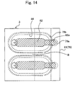
- a groove 79b may be extended from a recess 79a formed in the vibration plate 79 on the side of the cavity plate, up to a portion between a pressure chamber 44 corresponding to an individual electrode 62 having the contact section 62a facing the recess 79a and another pressure chamber 44 adjacent to this pressure chamber 44.
- the groove 79b may extend up to the shortest portion (area B) of a distance between the pressure chambers.
- the recess 79a and the groove 79b can be formed at the same time by half etching.
- the recess 79b exists between the plurality of pressure chambers, it is possible to suppress a phenomenon (cross talk) which occurs while operating the pressure chambers 44 and in which the deformation of the vibration plate 79 and the piezoelectric layer 61 in an area facing a pressure chamber 44 is propagated to the vibration plate 79 and the piezoelectric layer 61 in an area facing other pressure chamber 44. Accordingly, ink-discharge characteristic of the ink-jet head 3 is improved and a quality of printing is improved. To suppress the cross talk assuredly, it is desirable that the groove 79b, as shown in Fig. 14, is a groove having a shape of a ring surrounding each of the pressure chambers 44.
- the vibration plate 60 (74) is formed of an electroconductive metallic material so as to serves also as a common electrode.
- a vibration plate 60' may be formed by an insulating material and a common electrode (first electrode) 112 may be formed on the vibration plate 60'.
- an insulating layer may be provided on the vibration plate 60 (74) and the common electrode (first electrode) may be provided on the insulating layer.
Landscapes
- Engineering & Computer Science (AREA)
- Manufacturing & Machinery (AREA)
- Physics & Mathematics (AREA)
- Optics & Photonics (AREA)
- Microelectronics & Electronic Packaging (AREA)
- Particle Formation And Scattering Control In Inkjet Printers (AREA)
- Apparatuses For Generation Of Mechanical Vibrations (AREA)
- General Electrical Machinery Utilizing Piezoelectricity, Electrostriction Or Magnetostriction (AREA)
Applications Claiming Priority (1)
| Application Number | Priority Date | Filing Date | Title |
|---|---|---|---|
| JP2004329265 | 2004-11-12 |
Publications (3)
| Publication Number | Publication Date |
|---|---|
| EP1657059A2 true EP1657059A2 (de) | 2006-05-17 |
| EP1657059A3 EP1657059A3 (de) | 2007-04-04 |
| EP1657059B1 EP1657059B1 (de) | 2010-11-03 |
Family
ID=35652380
Family Applications (1)
| Application Number | Title | Priority Date | Filing Date |
|---|---|---|---|
| EP05024717A Expired - Lifetime EP1657059B1 (de) | 2004-11-12 | 2005-11-11 | Piezoelektrischer Aktor, Verfahren zur Herstellung eines piezoelektrischen Aktors, und Flüssigkeitstransportgerät |
Country Status (3)
| Country | Link |
|---|---|
| US (2) | US7358643B2 (de) |
| EP (1) | EP1657059B1 (de) |
| DE (1) | DE602005024499D1 (de) |
Cited By (3)
| Publication number | Priority date | Publication date | Assignee | Title |
|---|---|---|---|---|
| EP1759852A3 (de) * | 2005-08-31 | 2008-03-26 | Brother Kogyo Kabushiki Kaisha | Flüssigkeitstropfenausstossgerät und Flüssigkeitstransportgerät |
| CN107867073A (zh) * | 2016-09-28 | 2018-04-03 | 兄弟工业株式会社 | 致动器装置及制造方法、导线构件连接结构、液体喷射器 |
| EP3175989A4 (de) * | 2014-07-30 | 2018-04-25 | Kyocera Corporation | Tintenstrahlkopf und drucker |
Families Citing this family (7)
| Publication number | Priority date | Publication date | Assignee | Title |
|---|---|---|---|---|
| US7479729B2 (en) | 2004-05-19 | 2009-01-20 | Brother Kogyo Kabushiki Kaisha | Piezoelectric actuator, ink-jet head provided with the same, ink-jet printer, and method for manufacturing piezoelectric actuator |
| DE602005024499D1 (de) * | 2004-11-12 | 2010-12-16 | Brother Ind Ltd | Piezoelektrischer Aktor, Verfahren zur Herstellung eines piezoelektrischen Aktors, und Flüssigkeitstransportgerät |
| KR101153690B1 (ko) * | 2006-02-20 | 2012-06-18 | 삼성전기주식회사 | 잉크젯 헤드의 압전 액츄에이터 및 그 형성 방법 |
| US8220905B2 (en) * | 2006-08-23 | 2012-07-17 | Brother Kogyo Kabushiki Kaisha | Liquid transporting apparatus and method of producing liquid transporting apparatus |
| JP6011006B2 (ja) * | 2012-04-27 | 2016-10-19 | ブラザー工業株式会社 | 液滴噴射装置 |
| US8888254B2 (en) | 2012-09-13 | 2014-11-18 | Xerox Corporation | High density three-dimensional electrical interconnections |
| JP5983252B2 (ja) | 2012-09-28 | 2016-08-31 | ブラザー工業株式会社 | 液体吐出装置、基板の接続構造、及び、液体吐出装置の製造方法 |
Family Cites Families (10)
| Publication number | Priority date | Publication date | Assignee | Title |
|---|---|---|---|---|
| WO2004093183A1 (ja) * | 1995-03-17 | 2004-10-28 | Atsushi Hino | フィルムキャリアおよびこれを用いた半導体装置 |
| JP2001024248A (ja) * | 1999-07-07 | 2001-01-26 | Samsung Electro Mech Co Ltd | 低温焼成法による多層圧電/電歪セラミックアクチュエータの製造方法及びその方法によって製造された多層圧電/電歪セラミックアクチュエータ |
| US6740950B2 (en) * | 2001-01-15 | 2004-05-25 | Amkor Technology, Inc. | Optical device packages having improved conductor efficiency, optical coupling and thermal transfer |
| JP3603828B2 (ja) * | 2001-05-28 | 2004-12-22 | 富士ゼロックス株式会社 | インクジェット式記録ヘッド及びその製造方法並びにインクジェット式記録装置 |
| JP4362996B2 (ja) * | 2001-08-22 | 2009-11-11 | 富士ゼロックス株式会社 | 格子状配列構造の圧電/電歪アクチュエータ及びその製造方法 |
| JP2003162515A (ja) | 2001-11-22 | 2003-06-06 | Fujitsu Ltd | クラスタシステム |
| JP2003198068A (ja) * | 2001-12-27 | 2003-07-11 | Nec Corp | プリント基板、半導体装置、およびプリント基板と部品との電気的接続構造 |
| US6969157B2 (en) * | 2002-05-31 | 2005-11-29 | Matsushita Electric Industrial Co., Ltd. | Piezoelectric element, ink jet head, angular velocity sensor, method for manufacturing the same, and ink jet recording apparatus |
| DE602005024499D1 (de) * | 2004-11-12 | 2010-12-16 | Brother Ind Ltd | Piezoelektrischer Aktor, Verfahren zur Herstellung eines piezoelektrischen Aktors, und Flüssigkeitstransportgerät |
| JP5162871B2 (ja) * | 2006-09-27 | 2013-03-13 | ブラザー工業株式会社 | 液滴吐出装置用ヘッドの駆動方法および液滴吐出装置用ヘッド |
-
2005
- 2005-11-11 DE DE602005024499T patent/DE602005024499D1/de not_active Expired - Lifetime
- 2005-11-11 EP EP05024717A patent/EP1657059B1/de not_active Expired - Lifetime
- 2005-11-14 US US11/273,062 patent/US7358643B2/en not_active Expired - Lifetime
-
2008
- 2008-02-19 US US12/070,407 patent/US7560852B2/en not_active Expired - Fee Related
Cited By (6)
| Publication number | Priority date | Publication date | Assignee | Title |
|---|---|---|---|---|
| EP1759852A3 (de) * | 2005-08-31 | 2008-03-26 | Brother Kogyo Kabushiki Kaisha | Flüssigkeitstropfenausstossgerät und Flüssigkeitstransportgerät |
| US7559633B2 (en) | 2005-08-31 | 2009-07-14 | Brother Kogyo Kabushiki Kaisha | Liquid-droplet jetting apparatus and liquid transporting apparatus |
| EP3175989A4 (de) * | 2014-07-30 | 2018-04-25 | Kyocera Corporation | Tintenstrahlkopf und drucker |
| US10086611B2 (en) | 2014-07-30 | 2018-10-02 | Kyocera Corporation | Inkjet head and printer |
| CN107867073A (zh) * | 2016-09-28 | 2018-04-03 | 兄弟工业株式会社 | 致动器装置及制造方法、导线构件连接结构、液体喷射器 |
| US10875301B2 (en) | 2016-09-28 | 2020-12-29 | Brother Kogyo Kabushiki Kaisha | Method of manufacturing an actuator device |
Also Published As
| Publication number | Publication date |
|---|---|
| EP1657059B1 (de) | 2010-11-03 |
| DE602005024499D1 (de) | 2010-12-16 |
| US20080157628A1 (en) | 2008-07-03 |
| US7560852B2 (en) | 2009-07-14 |
| US20060103268A1 (en) | 2006-05-18 |
| EP1657059A3 (de) | 2007-04-04 |
| US7358643B2 (en) | 2008-04-15 |
Similar Documents
| Publication | Publication Date | Title |
|---|---|---|
| US7560852B2 (en) | Piezoelectric actuator, method for manufacturing piezoelectric actuator, and liquid transporting apparatus | |
| US7922300B2 (en) | Liquid ejecting apparatus, method for manufacturing liquid ejecting apparatus, and ink-jet printer | |
| US7980680B2 (en) | Method for manufacturing piezoelectric actuator, method for manufacturing liquid transporting apparatus, piezoelectric actuator, and liquid transporting apparatus | |
| JP5637197B2 (ja) | 圧電アクチュエータ、液体移送装置、及び、圧電アクチュエータの製造方法 | |
| US20080049077A1 (en) | Liquid transporting apparatus and method of producing liquid transporting apparatus | |
| US7976133B2 (en) | Liquid-jetting apparatus and method for producing the same | |
| JP4973377B2 (ja) | 液体移送装置及び液体移送装置の製造方法 | |
| JP2013060008A (ja) | 電気相互接続を形成するためのinsituフレキシブル回路エンボス加工 | |
| JP4887747B2 (ja) | 圧電アクチュエータ、圧電アクチュエータの製造方法、及び、液体移送装置 | |
| US7658474B2 (en) | Liquid transporting apparatus | |
| US7682000B2 (en) | Piezoelectric actuator, liquid transporting apparatus and method of producing piezoelectric actuator | |
| JP2008049569A (ja) | 液体移送装置及び液体移送装置の製造方法 | |
| EP1671797B1 (de) | Vorrichtung zum Transport von Flüssigkeiten und Verfahren zur Herstellung derselben | |
| CN1311972C (zh) | 压电喷墨头 | |
| JP2006116953A (ja) | 液体噴射装置及びその製造方法 | |
| US7559633B2 (en) | Liquid-droplet jetting apparatus and liquid transporting apparatus | |
| US7527364B2 (en) | Printer, liquid discharging head, and flexible flat cable of liquid discharging head | |
| JP2006304588A (ja) | 圧電アクチュエータ、液体移送装置、及び、圧電アクチュエータの製造方法 | |
| JP2006168004A (ja) | インクジェットヘッド及びその製造方法 | |
| JP2008036848A (ja) | 液体移送装置の製造方法、圧電アクチュエータの製造方法、液体移送装置、及び、圧電アクチュエータ |
Legal Events
| Date | Code | Title | Description |
|---|---|---|---|
| PUAI | Public reference made under article 153(3) epc to a published international application that has entered the european phase |
Free format text: ORIGINAL CODE: 0009012 |
|
| AK | Designated contracting states |
Kind code of ref document: A2 Designated state(s): AT BE BG CH CY CZ DE DK EE ES FI FR GB GR HU IE IS IT LI LT LU LV MC NL PL PT RO SE SI SK TR |
|
| AX | Request for extension of the european patent |
Extension state: AL BA HR MK YU |
|
| PUAL | Search report despatched |
Free format text: ORIGINAL CODE: 0009013 |
|
| AK | Designated contracting states |
Kind code of ref document: A3 Designated state(s): AT BE BG CH CY CZ DE DK EE ES FI FR GB GR HU IE IS IT LI LT LU LV MC NL PL PT RO SE SI SK TR |
|
| AX | Request for extension of the european patent |
Extension state: AL BA HR MK YU |
|
| 17P | Request for examination filed |
Effective date: 20070904 |
|
| AKX | Designation fees paid |
Designated state(s): DE FR GB |
|
| 17Q | First examination report despatched |
Effective date: 20080414 |
|
| GRAP | Despatch of communication of intention to grant a patent |
Free format text: ORIGINAL CODE: EPIDOSNIGR1 |
|
| GRAS | Grant fee paid |
Free format text: ORIGINAL CODE: EPIDOSNIGR3 |
|
| GRAA | (expected) grant |
Free format text: ORIGINAL CODE: 0009210 |
|
| AK | Designated contracting states |
Kind code of ref document: B1 Designated state(s): DE FR GB |
|
| REG | Reference to a national code |
Ref country code: GB Ref legal event code: FG4D |
|
| REF | Corresponds to: |
Ref document number: 602005024499 Country of ref document: DE Date of ref document: 20101216 Kind code of ref document: P |
|
| PLBE | No opposition filed within time limit |
Free format text: ORIGINAL CODE: 0009261 |
|
| STAA | Information on the status of an ep patent application or granted ep patent |
Free format text: STATUS: NO OPPOSITION FILED WITHIN TIME LIMIT |
|
| 26N | No opposition filed |
Effective date: 20110804 |
|
| REG | Reference to a national code |
Ref country code: DE Ref legal event code: R097 Ref document number: 602005024499 Country of ref document: DE Effective date: 20110804 |
|
| REG | Reference to a national code |
Ref country code: FR Ref legal event code: PLFP Year of fee payment: 11 |
|
| REG | Reference to a national code |
Ref country code: FR Ref legal event code: PLFP Year of fee payment: 12 |
|
| REG | Reference to a national code |
Ref country code: FR Ref legal event code: PLFP Year of fee payment: 13 |
|
| REG | Reference to a national code |
Ref country code: FR Ref legal event code: PLFP Year of fee payment: 14 |
|
| PGFP | Annual fee paid to national office [announced via postgrant information from national office to epo] |
Ref country code: DE Payment date: 20191017 Year of fee payment: 15 |
|
| PGFP | Annual fee paid to national office [announced via postgrant information from national office to epo] |
Ref country code: FR Payment date: 20191029 Year of fee payment: 15 |
|
| PGFP | Annual fee paid to national office [announced via postgrant information from national office to epo] |
Ref country code: GB Payment date: 20191029 Year of fee payment: 15 |
|
| REG | Reference to a national code |
Ref country code: DE Ref legal event code: R119 Ref document number: 602005024499 Country of ref document: DE |
|
| GBPC | Gb: european patent ceased through non-payment of renewal fee |
Effective date: 20201111 |
|
| PG25 | Lapsed in a contracting state [announced via postgrant information from national office to epo] |
Ref country code: FR Free format text: LAPSE BECAUSE OF NON-PAYMENT OF DUE FEES Effective date: 20201130 |
|
| PG25 | Lapsed in a contracting state [announced via postgrant information from national office to epo] |
Ref country code: GB Free format text: LAPSE BECAUSE OF NON-PAYMENT OF DUE FEES Effective date: 20201111 Ref country code: DE Free format text: LAPSE BECAUSE OF NON-PAYMENT OF DUE FEES Effective date: 20210601 |