EP1657734A2 - Appareil d'affichage à plasma avec un filtre - Google Patents
Appareil d'affichage à plasma avec un filtre Download PDFInfo
- Publication number
- EP1657734A2 EP1657734A2 EP05256926A EP05256926A EP1657734A2 EP 1657734 A2 EP1657734 A2 EP 1657734A2 EP 05256926 A EP05256926 A EP 05256926A EP 05256926 A EP05256926 A EP 05256926A EP 1657734 A2 EP1657734 A2 EP 1657734A2
- Authority
- EP
- European Patent Office
- Prior art keywords
- conduction layer
- coating film
- filter
- shield
- plasma display
- Prior art date
- Legal status (The legal status is an assumption and is not a legal conclusion. Google has not performed a legal analysis and makes no representation as to the accuracy of the status listed.)
- Withdrawn
Links
- 238000000576 coating method Methods 0.000 claims abstract description 103
- 239000011248 coating agent Substances 0.000 claims abstract description 95
- 239000010408 film Substances 0.000 claims description 106
- 239000011521 glass Substances 0.000 claims description 27
- 238000000034 method Methods 0.000 claims description 26
- 239000000463 material Substances 0.000 claims description 12
- 239000010409 thin film Substances 0.000 claims description 12
- 229910052804 chromium Inorganic materials 0.000 claims description 8
- 229910052802 copper Inorganic materials 0.000 claims description 8
- 229910052759 nickel Inorganic materials 0.000 claims description 8
- 238000000206 photolithography Methods 0.000 claims description 8
- 238000007650 screen-printing Methods 0.000 claims description 8
- 229910052709 silver Inorganic materials 0.000 claims description 8
- 238000004544 sputter deposition Methods 0.000 claims description 8
- 229910052719 titanium Inorganic materials 0.000 claims description 8
- 229910052725 zinc Inorganic materials 0.000 claims description 8
- 229910052782 aluminium Inorganic materials 0.000 claims description 4
- 229910052737 gold Inorganic materials 0.000 claims description 4
- 230000007423 decrease Effects 0.000 abstract description 4
- 238000004519 manufacturing process Methods 0.000 abstract description 3
- 230000005855 radiation Effects 0.000 abstract description 3
- 239000000758 substrate Substances 0.000 description 9
- 230000004888 barrier function Effects 0.000 description 6
- -1 Poly Ethylene Terephthalate Polymers 0.000 description 3
- 229920000139 polyethylene terephthalate Polymers 0.000 description 3
- 239000005020 polyethylene terephthalate Substances 0.000 description 3
- 239000002313 adhesive film Substances 0.000 description 2
- 238000010276 construction Methods 0.000 description 2
- CPBQJMYROZQQJC-UHFFFAOYSA-N helium neon Chemical compound [He].[Ne] CPBQJMYROZQQJC-UHFFFAOYSA-N 0.000 description 2
- 239000011261 inert gas Substances 0.000 description 2
- 238000009413 insulation Methods 0.000 description 2
- 239000000395 magnesium oxide Substances 0.000 description 2
- CPLXHLVBOLITMK-UHFFFAOYSA-N magnesium oxide Inorganic materials [Mg]=O CPLXHLVBOLITMK-UHFFFAOYSA-N 0.000 description 2
- AXZKOIWUVFPNLO-UHFFFAOYSA-N magnesium;oxygen(2-) Chemical compound [O-2].[Mg+2] AXZKOIWUVFPNLO-UHFFFAOYSA-N 0.000 description 2
- 239000007769 metal material Substances 0.000 description 2
- 229910052754 neon Inorganic materials 0.000 description 2
- 238000005192 partition Methods 0.000 description 2
- 238000002834 transmittance Methods 0.000 description 2
- OAICVXFJPJFONN-UHFFFAOYSA-N Phosphorus Chemical compound [P] OAICVXFJPJFONN-UHFFFAOYSA-N 0.000 description 1
- 229940081735 acetylcellulose Drugs 0.000 description 1
- 229920002301 cellulose acetate Polymers 0.000 description 1
- AMGQUBHHOARCQH-UHFFFAOYSA-N indium;oxotin Chemical compound [In].[Sn]=O AMGQUBHHOARCQH-UHFFFAOYSA-N 0.000 description 1
- 230000007257 malfunction Effects 0.000 description 1
- 239000011159 matrix material Substances 0.000 description 1
- GKAOGPIIYCISHV-UHFFFAOYSA-N neon atom Chemical compound [Ne] GKAOGPIIYCISHV-UHFFFAOYSA-N 0.000 description 1
- 239000011347 resin Substances 0.000 description 1
- 229920005989 resin Polymers 0.000 description 1
- 239000005361 soda-lime glass Substances 0.000 description 1
Images



Classifications
-
- H—ELECTRICITY
- H01—ELECTRIC ELEMENTS
- H01J—ELECTRIC DISCHARGE TUBES OR DISCHARGE LAMPS
- H01J11/00—Gas-filled discharge tubes with alternating current induction of the discharge, e.g. alternating current plasma display panels [AC-PDP]; Gas-filled discharge tubes without any main electrode inside the vessel; Gas-filled discharge tubes with at least one main electrode outside the vessel
- H01J11/20—Constructional details
- H01J11/34—Vessels, containers or parts thereof, e.g. substrates
- H01J11/44—Optical arrangements or shielding arrangements, e.g. filters, black matrices, light reflecting means or electromagnetic shielding means
-
- H—ELECTRICITY
- H01—ELECTRIC ELEMENTS
- H01J—ELECTRIC DISCHARGE TUBES OR DISCHARGE LAMPS
- H01J11/00—Gas-filled discharge tubes with alternating current induction of the discharge, e.g. alternating current plasma display panels [AC-PDP]; Gas-filled discharge tubes without any main electrode inside the vessel; Gas-filled discharge tubes with at least one main electrode outside the vessel
- H01J11/10—AC-PDPs with at least one main electrode being out of contact with the plasma
- H01J11/12—AC-PDPs with at least one main electrode being out of contact with the plasma with main electrodes provided on both sides of the discharge space
-
- H—ELECTRICITY
- H05—ELECTRIC TECHNIQUES NOT OTHERWISE PROVIDED FOR
- H05K—PRINTED CIRCUITS; CASINGS OR CONSTRUCTIONAL DETAILS OF ELECTRIC APPARATUS; MANUFACTURE OF ASSEMBLAGES OF ELECTRICAL COMPONENTS
- H05K9/00—Screening of apparatus or components against electric or magnetic fields
- H05K9/0073—Shielding materials
- H05K9/0094—Shielding materials being light-transmitting, e.g. transparent, translucent
- H05K9/0096—Shielding materials being light-transmitting, e.g. transparent, translucent for television displays, e.g. plasma display panel
-
- H—ELECTRICITY
- H01—ELECTRIC ELEMENTS
- H01J—ELECTRIC DISCHARGE TUBES OR DISCHARGE LAMPS
- H01J2211/00—Plasma display panels with alternate current induction of the discharge, e.g. AC-PDPs
- H01J2211/20—Constructional details
- H01J2211/34—Vessels, containers or parts thereof, e.g. substrates
- H01J2211/44—Optical arrangements or shielding arrangements, e.g. filters or lenses
- H01J2211/446—Electromagnetic shielding means; Antistatic means
Definitions
- the present invention relates to a plasma display apparatus. It more particularly relates to plasma display apparatus comprising a filter.
- a conventional plasma display panel comprises a front substrate and a rear substrate made of soda-lime glass. Barrier ribs formed between the front substrate and the rear substrate partition discharge cells.
- An inert gas injected into the discharge cells such as helium-xeon (He-Xe) or helium-neon (He-Ne), is excited with a high frequency voltage to generate a discharge.
- He-Xe helium-xeon
- He-Ne helium-neon
- Vacuum ultraviolet rays excite phosphors formed between the barrier ribs, thus displaying images.
- FIG. 1 is a perspective view schematically showing the construction of a conventional plasma display panel of the prior art.
- the plasma display panel in the prior art comprises a front panel and a rear panel.
- the front panel comprises a front glass substrate 10 and the rear panel comprises a rear glass substrate 20.
- the front panel and the rear panel are parallel to each other with a predetermined distance therebetween.
- a sustain electrode pair 11 and 12 for sustaining the emission of a cell through mutual discharge is formed on the front glass substrate 10.
- the sustain electrode pair comprises the scan electrode 11 and the sustain electrode 12.
- the scan electrode 11 comprises a transparent electrode 11a formed of a transparent ITO material and a bus electrode 11b formed of a metal material.
- the sustain electrode 12 comprises a transparent electrode 12a formed of a transparent ITO material and a bus electrode 12b formed of a metal material.
- the scan electrode 11 receives a scan signal for scanning a panel and a sustain signal for sustaining a discharge.
- the sustain electrode 12 receives a sustain signal.
- a dielectric layer 13a is formed on the sustain electrode pair 11, 12, and it functions to limit the discharge current and provides insulation between the electrode pairs.
- a protection layer 14 is formed on a top surface of the dielectric layer 13a and is formed of magnesium oxide (MgO) to facilitate a discharge condition.
- Address electrodes 22 intersecting the sustain electrode pair 11, 12 are disposed on the rear glass substrate 20.
- a dielectric layer 13b is formed on the address electrodes 22 and functions to provide insulation between the address electrodes 22.
- Barrier ribs 21 are formed on the dielectric layer 13b and partition discharge cells.
- R, G and B phosphor layer 23 are coated between the barrier ribs 21 and the barrier ribs 21 and radiate a visible ray for displaying images.
- a black matrix 21a that has a light shielding function of reducing reflection by absorbing external light generated outside the front glass 10 and a function of improving color purity and contrast of the front glass 10 is arranged on each of the barrier ribs.
- the plasma display panel constructed above implements images by applying a high voltage and a high frequency for a plasma discharge. Therefore, a problem arises because significant Electromagnetic Interference (EMI) is generated on the entire surface of the glass substrate.
- EMI Electromagnetic Interference
- the plasma display panel in the prior art radiates Near Infrared (NIR) induced by an inert gas such as Ne or Xe.
- NIR Near Infrared
- the NIR wavelength is problematic in that it causes the malfunction of electric home appliances since it is similar to a wavelength of the remote controls typically with electric home appliances.
- a glass filter or a film type filter is disposed at the front of the plasma display panel in the prior art.
- the EMI coating film formed in the glass filter in the prior art is formed as shown in FIGS. 2a and 2b.
- FIG. 2a shows the glass filter comprising the EMI coating film in the prior art.
- FIG. 2b is a plan view of the EMI coating film in the prior art.
- the glass filter 200 comprising the EMI coating film in the prior art comprises an Anti-Reflection (AR) coating film 210 for reducing ultraviolet rays and external reflection light, a NIR coating film 230 for NIR shielding, and an EMI coating film 250 for EMI shielding.
- the glass filter 200 has a glass 220 formed between the AR coating film 210, and the NIR coating film 230 and the EMI coating film 250.
- the AR coating film 210, the NIR coating film 230 and the EMI coating film 250 are attached to base coating films 240a, 240b and 240c, respectively.
- the base coating films 240a and 240b are combined with adhesive films 270a and 270b.
- a black frame 260 is formed in the adhesive film 270b attached to the glass 220.
- the EMI coating film 250 in the prior art comprises a conductive mesh 203 for shielding EMI, and a ground part 201 formed on the circumference of the EMI coating film 250 in order to ground the conductive mesh 203.
- the bias angle ( ⁇ ) In the prior art EMI coating film, the bias angle ( ⁇ ) must be controlled to prevent the Moire phenomenon due to the mesh 203. In the prior art EMI coating film, since the ground part 201 has to be aligned with the plasma display panel, it is difficult to control the bias angle ( ⁇ ).
- the prior art EMI coating film has problems in that the cost of a mask rises and the manufacturing cost of the EMI coating film rises.
- the film type filter can be attached on the entire surface of the plasma display panel.
- the film filter comprises the EMI coating film as shown in FIG. 2b in the same manner as the glass filter, the aforementioned same problems occur.
- the present invention seeks to provide an improved plasma display apparatus.
- a plasma display apparatus comprises a plasma display panel, and a filter comprising an EMI coating film which comprises a transparent conduction layer and a shield conduction layer formed on the transparent conduction layer and having a number of holes formed therein, wherein the filter is disposed on the plasma display panel.
- a filter comprises a transparent conduction layer, and an EMI coating film comprising a shield conduction layer which is formed on the transparent conduction layer and has a number of holes formed therein.
- an EMI coating film comprises a transparent conduction layer, and an EMI coating film comprising a shield conduction layer which is formed on the transparent conduction layer and has a number of holes formed therein.
- a plasma display apparatus comprises a plasma display panel, and a filter comprising an EMI coating film which comprises a transparent conduction layer and a shield conduction layer formed on a transparent conduction layer and having a number of holes formed therein, wherein the filter is disposed on the plasma display panel.
- the filter may be a glass filter or a film filter.
- the shield conduction layer may be a mesh type shield conduction layer.
- a mesh pitch of the shield conduction layer may be 500 ⁇ m to 1000 ⁇ m.
- the transparent conduction layer may comprise any one of ITO, ZnO or ATO.
- the shield conduction layer may comprise any one of each oxide material of Cu, Ag, Ni, Ti, Zn, Cr, A1 or Au.
- the shield conduction layer may be formed by any one of a sputtering method, a screen printing method, a wet coating method, a thin film sheet junction method or a photolithography method.
- a filter comprises a transparent conduction layer, and an EMI coating film comprising a shield conduction layer which is formed on the transparent conduction layer and has a number of holes formed therein.
- the filter may be either a glass filter or a film filter.
- the shield conduction layer may be a mesh type shield conduction layer.
- the mesh pitch of the shield conduction layer may be 500 ⁇ m to 1000 ⁇ m.
- the transparent conduction layer may comprise any one of ITO, ZnO or ATO.
- the shield conduction layer may comprise any one of each oxide material of Cu, Ag, Ni, Ti, Zn, Cr, A1 or Au.
- the shield conduction layer may be formed by any one of a sputtering method, a screen printing method, a wet coating method, a thin film sheet junction method or a photolithography method.
- an EMI coating film comprises a transparent conduction layer, and an EMI coating film comprising a shield conduction layer which is formed on the transparent conduction layer and has a number of holes formed therein.
- the shield conduction layer may be a mesh type shield conduction layer.
- the mesh pitch of the shield conduction layer may be 500 ⁇ m to 1000 ⁇ m.
- the transparent conduction layer may comprise any one of ITO, ZnO or ATO.
- the shield conduction layer may comprise any one of each oxide material of Cu, Ag, Ni, Ti, Zn, Cr, Al or Au.
- the shield conduction layer may be formed by any one of a sputtering method, a screen printing method, a wet coating method, a thin film sheet junction method or a photolithography method.
- FIG. 1 is a perspective view schematically showing the construction of a plasma display panel in the prior art
- FIG. 2a shows a glass filter comprising an EMI coating film in the prior art
- FIG. 2b is a plan view of the EMI coating film in the prior art
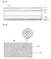
- FIG. 3a shows a glass filter comprising an EMI coating film according to an embodiment of the present invention
- FIG. 3b is a plan view of the EMI coating film according to an embodiment of the present invention.
- FIG. 4 shows a film filter comprising an EMI coating film according to an embodiment of the present invention.
- a glass filter 300 comprises a glass 320, an AR coating film 310 for shielding ultraviolet radiation and reducing external reflection light, an NIR coating film 310 for shielding NIR, an EMI coating film 350 for shielding EMI, and a color dye layer 330 for shielding neon (Ne).
- the color dye layer 330 shields light of a specific color, which is generated due to Ne when the plasma display panel is driven.
- One side of the color dye layer 330 is brought in contact with one side of the glass 320.
- the color dye layer 330 and the glass 320 are combined through a surface contact.
- a first base coating film 340a is comprised of a material such as Poly Ethylene Terephthalate (PET) or Triacetyl Acetyl Cellulose (TAC).
- PET Poly Ethylene Terephthalate
- TAC Triacetyl Acetyl Cellulose
- the AR coating film and the NIR coating film are integrated into one film 310 in order to shield the ultraviolet rays, reduce external reflection light and shield NIR.
- One side of the AR coating film and the NIR coating film is brought in contact with the other side of the base coating film 340a.
- a second base coating film 340b is comprised of a material such as PET or TAC and is brought in contact with the other side of the glass 320.
- the EMI coating film 350 is formed to shield EMI and is brought in contact with the other side of the second base coating film 340b.
- the EMI coating film 350 comprises a transparent conduction layer 350a formed of a material, such as Indium Tin Oxide (ITO) ZnO or ATO, and a shield conduction layer 350b, which is formed on the transparent conduction layer 350a and has a number of holes formed therein.
- the shield conduction layer 350b of the EMI coating film according to the present embodiment is a mesh type shield conduction layer.
- the transparent conduction layer 350a is connected to the ground so that the shield conduction layer 350b is grounded, instead of the ground part 201 comprised in the EMI coating film 250 in the prior art, which is shown in FIG. 2b. Since the transparent conduction layer 350a is connected to the ground and the shield conduction layer 350b is grounded according as described above, the mesh pitch of the shield conduction layers 350b is more than the mesh pitch of the prior art.
- the mesh pitch is small.
- the mesh pitch in embodiments of the present invention can be set to 500 ⁇ m to 1000 ⁇ m.
- the shield conduction layer 350b is formed using an inexpensive cheap mask.
- the shield conduction layer 350b is formed using conductive oxide such as Cu, Ag, Ni, Ti, Zn, Cr, A1 or Au by any one of a sputtering method, a screen printing method, a wet coating method, a thin film sheet junction method or a photolithography method.
- the shield conduction layer 350b is formed on the transparent conduction layer 350a using a thin film sheet in which the shield conduction layer 350b is previously formed.
- the glass filter comprising the EMI coating film is disposed on the plasma display panel, thus forming the plasma display apparatus.
- a film filter 400 comprises an AR coating film for shielding ultraviolet radiation and reducing external reflection light, a NIR coating film for shielding NIR, an EMI coating film 450 for shielding EMI, and a color dye layer 430 for shielding Ne.
- the function of each of the films is the same as that of the first embodiment. Description thereof will therefore be omitted.
- the AR coating film and the NIR coating film are integrated into one film 410.
- a third base coating film 440a is formed between the AR coating film and the NIR coating film, and the color dye layer 430.
- the EMI coating film 450 according to the present embodiment is formed between a transparent processing resin 460 and a fourth base coating film 440b.
- the EMI coating film 450 comprised in the film filter 400 according to the present embodiment comprises a transparent conduction layer 450a formed of a material, such as ITO, ZnO or ATO, and a shield conduction layer 450b, which is formed on the transparent conduction layer 450a and has a number of holes formed therein.
- the shield conduction layer 450b of the EMI coating film is a mesh type shield conduction layer.
- the transparent conduction layer 450a is connected to the ground so that the shield conduction layer 450b is grounded, instead of the ground part 201 comprised in the EMI coating film 250 in the prior art, which is shown in FIG. 2b. Since the transparent conduction layer 450a is connected to the ground and the shield conduction layer 450b is grounded according as described above, the mesh pitch of the shield conduction layers 450b is greater than the mesh pitch of the prior art.
- the mesh pitch is small.
- the mesh pitch in the present embodiment can be set to 500 ⁇ m to 1000 ⁇ m.
- the EMI coating film according to the present embodiment can improve the contrast of the plasma display panel.
- the bias angle ( ⁇ ) is controlled by only rotating the EMI coating film according to an embodiment of the present invention.
- the shield conduction layer 450b is formed using an inexpensive mask.
- the shield conduction layer 450b is formed using conductive oxide such as Cu, Ag, Ni, Ti, Zn, Cr, A1 or Au by any one of a sputtering method, a screen printing method, a wet coating method, a thin film sheet junction method or a photolithography method.
- the shield conduction layer 450b is formed on the transparent conduction layer 450a using a thin film sheet in which the shield conduction layer 450b is previously formed.
- the film filter comprising the EMI coating film according to an embodiment of the present invention is disposed on the plasma display panel, thus forming the plasma display apparatus.
Landscapes
- Physics & Mathematics (AREA)
- Engineering & Computer Science (AREA)
- Plasma & Fusion (AREA)
- Electromagnetism (AREA)
- Microelectronics & Electronic Packaging (AREA)
- Devices For Indicating Variable Information By Combining Individual Elements (AREA)
- Shielding Devices Or Components To Electric Or Magnetic Fields (AREA)
- Gas-Filled Discharge Tubes (AREA)
Applications Claiming Priority (1)
| Application Number | Priority Date | Filing Date | Title |
|---|---|---|---|
| KR1020040092150A KR100738212B1 (ko) | 2004-11-11 | 2004-11-11 | 플라즈마 디스플레이 패널 |
Publications (2)
| Publication Number | Publication Date |
|---|---|
| EP1657734A2 true EP1657734A2 (fr) | 2006-05-17 |
| EP1657734A3 EP1657734A3 (fr) | 2008-07-16 |
Family
ID=35788587
Family Applications (1)
| Application Number | Title | Priority Date | Filing Date |
|---|---|---|---|
| EP05256926A Withdrawn EP1657734A3 (fr) | 2004-11-11 | 2005-11-09 | Appareil d'affichage à plasma avec un filtre |
Country Status (5)
| Country | Link |
|---|---|
| US (1) | US20060097650A1 (fr) |
| EP (1) | EP1657734A3 (fr) |
| JP (1) | JP2006139277A (fr) |
| KR (1) | KR100738212B1 (fr) |
| CN (1) | CN1773660A (fr) |
Cited By (1)
| Publication number | Priority date | Publication date | Assignee | Title |
|---|---|---|---|---|
| WO2011018084A3 (fr) * | 2009-08-11 | 2011-04-21 | Goecke Ludwig | Matériau de blindage contre des ondes électromagnétiques |
Families Citing this family (11)
| Publication number | Priority date | Publication date | Assignee | Title |
|---|---|---|---|---|
| KR100769907B1 (ko) * | 2006-07-12 | 2007-10-24 | 엘지전자 주식회사 | 플라즈마 디스플레이 장치 |
| KR100791205B1 (ko) * | 2006-11-09 | 2008-01-02 | 에스케이씨하스디스플레이필름(주) | 디스플레이 패널용 광학 필터 및 이의 제조방법 |
| KR100791211B1 (ko) * | 2006-11-13 | 2008-01-03 | 에스케이씨하스디스플레이필름(주) | 디스플레이 패널용 광학 필터 및 이의 제조방법 |
| KR20080054204A (ko) * | 2006-12-12 | 2008-06-17 | 삼성코닝정밀유리 주식회사 | 디스플레이 장치용 복합 필름 및 이를 포함하는 디스플레이장치 |
| KR100893617B1 (ko) * | 2007-05-23 | 2009-04-20 | 삼성에스디아이 주식회사 | 플라즈마 디스플레이 패널 및 필터 |
| WO2010036776A2 (fr) * | 2008-09-24 | 2010-04-01 | Alliance For Sustainable Energy, Llc | Dispositifs électroniques à couche mince présentant des barrières conductrices et transparentes de perméation à la diffusion du gaz et de l'humidité |
| US9302452B2 (en) | 2012-03-02 | 2016-04-05 | Ppg Industries Ohio, Inc. | Transparent laminates comprising inkjet printed conductive lines and methods of forming the same |
| WO2016152581A1 (fr) | 2015-03-25 | 2016-09-29 | 株式会社アルバック | Substrat conducteur transparent et structure multicouche transparente |
| US9986669B2 (en) * | 2015-11-25 | 2018-05-29 | Ppg Industries Ohio, Inc. | Transparency including conductive mesh including a closed shape having at least one curved side |
| USD878060S1 (en) * | 2017-09-06 | 2020-03-17 | Jaguar Land Rover Limited | Template for a vehicle |
| US11745702B2 (en) | 2018-12-11 | 2023-09-05 | Ppg Industries Ohio, Inc. | Coating including electrically conductive lines directly on electrically conductive layer |
Citations (2)
| Publication number | Priority date | Publication date | Assignee | Title |
|---|---|---|---|---|
| EP0930637A2 (fr) | 1997-12-22 | 1999-07-21 | Bridgestone Corporation | Ecran contre les ondes électromagnétiques, plaque transparente ainsi que panneau de visualisation |
| EP0963146A1 (fr) | 1997-12-24 | 1999-12-08 | Gunze Limited | Element transparent de blindage contre des ondes electromagnetiques et son procede de production |
Family Cites Families (9)
| Publication number | Priority date | Publication date | Assignee | Title |
|---|---|---|---|---|
| TW417025B (en) * | 1997-04-10 | 2001-01-01 | Sumitomo Chemical Co | Front plate for plasma display |
| DE69838762T2 (de) * | 1997-06-24 | 2008-04-30 | Bridgestone Corp. | Elektromagnetische Wellen abschirmende lichtdurchlässige Platte |
| US6255778B1 (en) * | 1997-10-13 | 2001-07-03 | Bridgestone Corporation | Plasma display panel having electromagnetic wave shielding material attached to front surface of display |
| KR100654114B1 (ko) * | 1998-10-30 | 2006-12-05 | 스미또모 가가꾸 가부시끼가이샤 | 전자파 차단판 |
| KR100521911B1 (ko) * | 2001-07-09 | 2005-10-13 | 다이니폰 인사츠 가부시키가이샤 | 전자파 차폐용 부재 및 그 제조방법 |
| KR20040075496A (ko) * | 2003-02-21 | 2004-08-30 | 엘지전자 주식회사 | Pdp 전자파 차폐용 도전성 필터 제조방법 |
| KR20040085766A (ko) * | 2003-04-01 | 2004-10-08 | 엘지전자 주식회사 | 플라즈마 디스플레이 패널의 전자파 차폐막 |
| KR100751932B1 (ko) * | 2003-04-01 | 2007-08-27 | 엘지전자 주식회사 | 전면 필터와 그의 제조 방법 |
| KR100509764B1 (ko) * | 2003-04-10 | 2005-08-25 | 엘지전자 주식회사 | 전자파 차폐 필터 및 그 제조 방법 |
-
2004
- 2004-11-11 KR KR1020040092150A patent/KR100738212B1/ko not_active Expired - Fee Related
-
2005
- 2005-11-04 JP JP2005320340A patent/JP2006139277A/ja not_active Withdrawn
- 2005-11-09 EP EP05256926A patent/EP1657734A3/fr not_active Withdrawn
- 2005-11-10 US US11/270,474 patent/US20060097650A1/en not_active Abandoned
- 2005-11-11 CN CNA2005101182008A patent/CN1773660A/zh active Pending
Patent Citations (2)
| Publication number | Priority date | Publication date | Assignee | Title |
|---|---|---|---|---|
| EP0930637A2 (fr) | 1997-12-22 | 1999-07-21 | Bridgestone Corporation | Ecran contre les ondes électromagnétiques, plaque transparente ainsi que panneau de visualisation |
| EP0963146A1 (fr) | 1997-12-24 | 1999-12-08 | Gunze Limited | Element transparent de blindage contre des ondes electromagnetiques et son procede de production |
Cited By (2)
| Publication number | Priority date | Publication date | Assignee | Title |
|---|---|---|---|---|
| WO2011018084A3 (fr) * | 2009-08-11 | 2011-04-21 | Goecke Ludwig | Matériau de blindage contre des ondes électromagnétiques |
| CN102498495A (zh) * | 2009-08-11 | 2012-06-13 | 哈戈技术控股有限公司 | 用于屏蔽电磁波的材料 |
Also Published As
| Publication number | Publication date |
|---|---|
| US20060097650A1 (en) | 2006-05-11 |
| KR20060045104A (ko) | 2006-05-16 |
| KR100738212B1 (ko) | 2007-07-12 |
| EP1657734A3 (fr) | 2008-07-16 |
| CN1773660A (zh) | 2006-05-17 |
| JP2006139277A (ja) | 2006-06-01 |
Similar Documents
| Publication | Publication Date | Title |
|---|---|---|
| KR100509763B1 (ko) | 플라즈마 디스플레이 패널의 전면필터 | |
| KR100926712B1 (ko) | 전면 필터와 그의 제조 방법 | |
| US8013956B2 (en) | Front filter in a flat panel display device | |
| US7362043B2 (en) | Plasma display panel having a grounding structure of a film type front surface filter | |
| KR20040085699A (ko) | 플라즈마 디스플레이 패널의 전면필터 | |
| US20060097650A1 (en) | Plasma display apparatus comprising filter | |
| CN101714314A (zh) | 等离子体显示装置 | |
| US8390929B2 (en) | Display panel and optical filter which control transmittance color and reflection color | |
| EP1755139B1 (fr) | Appareil d'affichage à plasma | |
| US8053963B2 (en) | Display device and optical filter | |
| MX2007009089A (es) | Capa protectora contra la luz externa y aparato de visualización que la contiene. | |
| KR100709879B1 (ko) | 플라즈마 디스플레이 패널의 필름형 필터 | |
| KR100533423B1 (ko) | 플라즈마 디스플레이 패널 | |
| US20060244678A1 (en) | Filter for display apparatus and plasma display apparatus comprising filter | |
| US20090058298A1 (en) | Plasma display panel and method of fabricating the same | |
| KR20050106622A (ko) | 플라즈마 표시장치 및 그 제조방법 | |
| KR100822211B1 (ko) | 플라즈마 디스플레이 패널 | |
| KR100509597B1 (ko) | 플라즈마 표시장치 | |
| KR20060059736A (ko) | 플라즈마 디스플레이 패널 | |
| KR100751416B1 (ko) | 플라즈마 디스플레이 패널 및 그 제작 방법 | |
| KR20050106623A (ko) | 플라즈마 표시장치 | |
| KR20060113147A (ko) | 필름형 전면필터 및 그 제조방법 | |
| KR20070116467A (ko) | 플라즈마 디스플레이 패널 및 그 제작 방법 | |
| KR20070108718A (ko) | 플라즈마 디스플레이 패널 | |
| KR20070056361A (ko) | 플라즈마 디스플레이 장치 |
Legal Events
| Date | Code | Title | Description |
|---|---|---|---|
| PUAI | Public reference made under article 153(3) epc to a published international application that has entered the european phase |
Free format text: ORIGINAL CODE: 0009012 |
|
| 17P | Request for examination filed |
Effective date: 20051116 |
|
| AK | Designated contracting states |
Kind code of ref document: A2 Designated state(s): AT BE BG CH CY CZ DE DK EE ES FI FR GB GR HU IE IS IT LI LT LU LV MC NL PL PT RO SE SI SK TR |
|
| AX | Request for extension of the european patent |
Extension state: AL BA HR MK YU |
|
| RIN1 | Information on inventor provided before grant (corrected) |
Inventor name: KIM, KYUNGKU,C/O HANGARAM SILLA APT.404-1006 |
|
| RIN1 | Information on inventor provided before grant (corrected) |
Inventor name: KIM, KYUNGKU,C/O HANGARAM SILLA APT.404-1006 |
|
| RIN1 | Information on inventor provided before grant (corrected) |
Inventor name: KIM, KYUNGKU,C/O HANGARAM SILLA APT.404-1006 |
|
| RIN1 | Information on inventor provided before grant (corrected) |
Inventor name: KIM, KYUNGKU,C/O HANGARAM SILLA APT.404-1006 |
|
| PUAL | Search report despatched |
Free format text: ORIGINAL CODE: 0009013 |
|
| AK | Designated contracting states |
Kind code of ref document: A3 Designated state(s): AT BE BG CH CY CZ DE DK EE ES FI FR GB GR HU IE IS IT LI LT LU LV MC NL PL PT RO SE SI SK TR |
|
| AX | Request for extension of the european patent |
Extension state: AL BA HR MK YU |
|
| RIC1 | Information provided on ipc code assigned before grant |
Ipc: H05K 9/00 20060101ALI20080612BHEP Ipc: H01J 17/49 20060101ALI20080612BHEP Ipc: H01J 17/16 20060101AFI20080612BHEP |
|
| STAA | Information on the status of an ep patent application or granted ep patent |
Free format text: STATUS: THE APPLICATION HAS BEEN WITHDRAWN |
|
| 18W | Application withdrawn |
Effective date: 20081205 |