EP1657740B1 - Siliciumcarbid-epitaxial-wafer, verfahren zur herstellung eines solchen wafers und auf einem solchen wafer ausgebildetes halbleiterbauelement - Google Patents
Siliciumcarbid-epitaxial-wafer, verfahren zur herstellung eines solchen wafers und auf einem solchen wafer ausgebildetes halbleiterbauelement Download PDFInfo
- Publication number
- EP1657740B1 EP1657740B1 EP04771855.6A EP04771855A EP1657740B1 EP 1657740 B1 EP1657740 B1 EP 1657740B1 EP 04771855 A EP04771855 A EP 04771855A EP 1657740 B1 EP1657740 B1 EP 1657740B1
- Authority
- EP
- European Patent Office
- Prior art keywords
- silicon carbide
- epitaxial wafer
- wafer
- substrate
- sic
- Prior art date
- Legal status (The legal status is an assumption and is not a legal conclusion. Google has not performed a legal analysis and makes no representation as to the accuracy of the status listed.)
- Expired - Lifetime
Links
Images


Classifications
-
- C—CHEMISTRY; METALLURGY
- C30—CRYSTAL GROWTH
- C30B—SINGLE-CRYSTAL GROWTH; UNIDIRECTIONAL SOLIDIFICATION OF EUTECTIC MATERIAL OR UNIDIRECTIONAL DEMIXING OF EUTECTOID MATERIAL; REFINING BY ZONE-MELTING OF MATERIAL; PRODUCTION OF A HOMOGENEOUS POLYCRYSTALLINE MATERIAL WITH DEFINED STRUCTURE; SINGLE CRYSTALS OR HOMOGENEOUS POLYCRYSTALLINE MATERIAL WITH DEFINED STRUCTURE; AFTER-TREATMENT OF SINGLE CRYSTALS OR A HOMOGENEOUS POLYCRYSTALLINE MATERIAL WITH DEFINED STRUCTURE; APPARATUS THEREFOR
- C30B25/00—Single-crystal growth by chemical reaction of reactive gases, e.g. chemical vapour-deposition growth
- C30B25/02—Epitaxial-layer growth
- C30B25/18—Epitaxial-layer growth characterised by the substrate
- C30B25/20—Epitaxial-layer growth characterised by the substrate the substrate being of the same materials as the epitaxial layer
-
- C—CHEMISTRY; METALLURGY
- C30—CRYSTAL GROWTH
- C30B—SINGLE-CRYSTAL GROWTH; UNIDIRECTIONAL SOLIDIFICATION OF EUTECTIC MATERIAL OR UNIDIRECTIONAL DEMIXING OF EUTECTOID MATERIAL; REFINING BY ZONE-MELTING OF MATERIAL; PRODUCTION OF A HOMOGENEOUS POLYCRYSTALLINE MATERIAL WITH DEFINED STRUCTURE; SINGLE CRYSTALS OR HOMOGENEOUS POLYCRYSTALLINE MATERIAL WITH DEFINED STRUCTURE; AFTER-TREATMENT OF SINGLE CRYSTALS OR A HOMOGENEOUS POLYCRYSTALLINE MATERIAL WITH DEFINED STRUCTURE; APPARATUS THEREFOR
- C30B29/00—Single crystals or homogeneous polycrystalline material with defined structure characterised by the material or by their shape
- C30B29/10—Inorganic compounds or compositions
- C30B29/36—Carbides
-
- H—ELECTRICITY
- H10—SEMICONDUCTOR DEVICES; ELECTRIC SOLID-STATE DEVICES NOT OTHERWISE PROVIDED FOR
- H10D—INORGANIC ELECTRIC SEMICONDUCTOR DEVICES
- H10D62/00—Semiconductor bodies, or regions thereof, of devices having potential barriers
- H10D62/40—Crystalline structures
- H10D62/405—Orientations of crystalline planes
-
- H—ELECTRICITY
- H10—SEMICONDUCTOR DEVICES; ELECTRIC SOLID-STATE DEVICES NOT OTHERWISE PROVIDED FOR
- H10D—INORGANIC ELECTRIC SEMICONDUCTOR DEVICES
- H10D62/00—Semiconductor bodies, or regions thereof, of devices having potential barriers
- H10D62/80—Semiconductor bodies, or regions thereof, of devices having potential barriers characterised by the materials
- H10D62/83—Semiconductor bodies, or regions thereof, of devices having potential barriers characterised by the materials being Group IV materials, e.g. B-doped Si or undoped Ge
- H10D62/832—Semiconductor bodies, or regions thereof, of devices having potential barriers characterised by the materials being Group IV materials, e.g. B-doped Si or undoped Ge being Group IV materials comprising two or more elements, e.g. SiGe
- H10D62/8325—Silicon carbide
-
- Y—GENERAL TAGGING OF NEW TECHNOLOGICAL DEVELOPMENTS; GENERAL TAGGING OF CROSS-SECTIONAL TECHNOLOGIES SPANNING OVER SEVERAL SECTIONS OF THE IPC; TECHNICAL SUBJECTS COVERED BY FORMER USPC CROSS-REFERENCE ART COLLECTIONS [XRACs] AND DIGESTS
- Y10—TECHNICAL SUBJECTS COVERED BY FORMER USPC
- Y10S—TECHNICAL SUBJECTS COVERED BY FORMER USPC CROSS-REFERENCE ART COLLECTIONS [XRACs] AND DIGESTS
- Y10S438/00—Semiconductor device manufacturing: process
- Y10S438/931—Silicon carbide semiconductor
Definitions
- the present invention relates to a high-quality silicon carbide (SiC) epitaxial wafer obtained from the crystal growth of silicon carbide, manufacturing method of such wafer, and semiconductor device formed on this wafer.
- SiC silicon carbide
- SiC has various crystal structures, in the epitaxial growth of the SiC ⁇ 0001 ⁇ face, SiC having a different crystal structure easily gets mixed into the epitaxially grown portion.
- Patent Document 1 US Patent No. 4,912,064
- SiC has crystal defects extending in the ⁇ 0001 ⁇ direction and crystal defects extending in a direction perpendicular to the ⁇ 0001 ⁇ direction.
- Patent Document 1 since both crystal defects existing in the substrate are propagated to the epitaxially grown portion, it is difficult to reduce the defects in the wafer. This situation is shown in FIG. 1a .
- the (0001) Si face is used for epitaxial growth. Nevertheless, as the angle of the off substrate becomes small, during the epitaxial growth of the (0001) Si face, step bunching and two-dimensional nucleus formation will occur and the flatness of the epitaxially grown surface will be lost.
- EP 0462963 A1 discloses a silicon carbide substrate, process for producing the same, and semiconductor element containing silicon carbide substrate.
- an object of the present invention is to provide a method of manufacturing an epitaxial wafer having a highly flat surface while reducing the crystal defects in the SiC epitaxial wafer, the SiC epitaxial wafer obtained thereby, and a semiconductor device formed on such wafer.
- the present inventors achieved the present invention by discovering that the foregoing defects can be reduced by adjusting the off angle from the ⁇ 0001 ⁇ face of the SiC substrate, and controlling the growth pressure and composition ratio of the source gas.
- the present invention provides the following disclosure: 1) A silicon carbide epitaxial wafer which is formed on a substrate that is less than 1° off from the ⁇ 0001 ⁇ surface of silicon carbide having an ⁇ -type crystal structure. 2) The silicon carbide epitaxial wafer according to 1) above, wherein said silicon carbide epitaxial wafer is formed on a substrate of the (0001) C face. 3) The silicon carbide epitaxial wafer according to 1) or 2) above, wherein a silicon carbide substrate having a 4H crystal structure is used. 4) The silicon carbide epitaxial wafer according to any one of 1) to 3) above, wherein said silicon carbide epitaxial wafer has a flat surface.
- the present invention yields a superior effect in that an epitaxial wafer having a highly flat surface can be manufactured while reducing the crystals defects in the SiC epitaxial wafer.
- the present invention by manufacturing the epitaxial wafer with a SiC substrate whose off angle is less than 1° from the ⁇ 0001 ⁇ face, as shown in FIG. 1b , defects extending in a direction that is perpendicular to the ⁇ 0001 ⁇ direction existing in the substrate can be suppressed from propagating to the epitaxially grown portion, and crystal defects in the epitaxial wafer can be reduced thereby.
- the growth pressure to be 250mbar or less, and controlling the flow rate of the source gas so that the composition ratio of C and Si in source gases becomes 1 or less; in other words, by controlling the growth pressure to be 250mbar or less and the composition ratio of C and Si in source gases to be 1 or less while using the (0001) C face, deterioration in the flatness of the growth surface caused by step bunching or two-dimensional nucleus formation can be suppressed, and a wafer having a highly flat epitaxial wafer surface with reduced crystal defects can be manufactured thereby.
- FIG. 4 shows the surface of the epitaxial wafer after 5 hours of growth, and, by using the (0001) C face, there is no surface roughness caused by step bunching or two-dimensional nucleus formation, and a flat surface is formed thereby.
- FIG. 5a shows defects in the SiC substrate.
- the crystal defects extending in the ⁇ 0001 ⁇ direction visible as white dots in the SiC substrate.
- the present invention also enables the improvement in the yield of the SiC ingot.
- a SiC ingot is manufactured by growing in the ⁇ 0001 ⁇ direction.
- cutting stock of 10mm as shown in FIG. 6a will arise if the ingot has a diameter of 75mm (3 inches).
- the long-term reliability upon applying forward voltage of the semiconductor device can be improved.
- the crystal defects extending in a direction perpendicular to the ⁇ 0001 ⁇ direction in the epitaxial wafer will cause the forward current to decrease when the forward voltage is applied for a prolonged period of time.
- the epitaxial wafer manufactured according to the present invention since the crystal defects extending in a direction that is perpendicular to the ⁇ 0001 ⁇ direction in the epitaxial wafer have been reduced as described above, the forward current will not decrease even when applying forward voltage for a prolonged period of time, and a significant effect is yielded in that a highly reliable epitaxial wafer can be obtained.
- the channel resistance of the semiconductor device can be reduced.
- the MOSFET formed on the epitaxial wafer manufactured according to the present invention is capable of reducing the roughness in the oxide film/semiconductor interface.
- FIG. 2 shows the conceptual diagram of the series of growth processes of the present Examples.
- a 4H-SiC substrate inclined 0.5° from the (0001) C face to the [11 20] direction was used as the crystal growth substrate.
- the pressure in the reaction tube was controlled to be 250mbar while flowing 40slm of hydrogen gas in the reaction tube.
- the SiC substrate was heated via high-frequency induction heating, and heated from 1500°C to 1600°C while discharging 3.33sccm of propane gas. After heating the SiC substrate to 1600°C, this state was maintained for 3 minutes, and the SiC substrate surface was cleansed.
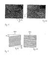
- FIG. 3 shows the atomic force microscopy of the cleansed SiC substrate surface.
- FIG. 3a is a planar image, and steps are aligned with regularity. The height thereof is 0.7nm from the cross sectional image of FIG. 3b .
- the composition ratio of C and Si in source gases was controlled to be 0.6 by introducing 6.67sccm of silane gas and 1.334sccm of propane gas, and epitaxial growth was performed on this SiC substrate in order to manufacture an epitaxial wafer.
- FIG. 4 shows the surface of the epitaxial wafer after 5 hours of growth.
- the present invention it is possible to manufacture an epitaxial wafer with a highly flat surface while reducing the crystal defects in the SiC epitaxial wafer, the cutting stock upon cutting the SiC ingot will hardly arise, and the yield can be improved thereby. Further, a significant effect is yielded in that a highly reliable epitaxial wafer can be obtained in which the forward current will not decrease even when forward voltage is applied for a prolonged period of time. Moreover, with a MOSFET formed on this epitaxial wafer, it is possible to reduce the roughness in the oxide film/semiconductor interface, and the channel mobility will increase. Thus, a superior effect is yielded in that the channel resistance of the semiconductor device will decrease, and this epitaxial wafer is extremely useful as the material of a semiconductor device or the like.
Landscapes
- Chemical & Material Sciences (AREA)
- Engineering & Computer Science (AREA)
- Crystallography & Structural Chemistry (AREA)
- Materials Engineering (AREA)
- Metallurgy (AREA)
- Organic Chemistry (AREA)
- Chemical Kinetics & Catalysis (AREA)
- General Chemical & Material Sciences (AREA)
- Inorganic Chemistry (AREA)
- Crystals, And After-Treatments Of Crystals (AREA)
- Chemical Vapour Deposition (AREA)
- Insulated Gate Type Field-Effect Transistor (AREA)
Claims (8)
- Siliciumcarbid-Epitaxial-Wafer, der auf einem Siliciumcarbid-Substrat mit einer Kristallstruktur des Typs 4H ausgebildet ist, dadurch gekennzeichnet, dass der Epitaxial-Wafer epitaxial auf einer Oberfläche des Siliciumcarbid-Substrats gezüchtet wurde, die 0,5° gegenüber der C-Fläche (0001) zur Richtung [1120] geneigt ist.
- Siliciumcarbid-Epitaxial-Wafer nach Anspruch 1, worin besagter Siliciumcarbid-Epitaxial-Wafer eine flache Oberfläche aufweist.
- Halbleiterbauelement, das auf dem Epitaxial-Wafer nach Anspruch 1 oder Anspruch 2 ausgebildet ist.
- Verfahren zur Herstellung eines Siliciumcarbid-Epitaxial-Wafers auf einer Oberfläche eines Siliciumcarbid-Substrats mit einer Kristallstruktur des Typs 4H, dadurch gekennzeichnet, dass der Wafer epitaxial auf einer Oberfläche des besagten Substrats gezüchtet wird, die weniger als 1° weg von der C-Fläche (0001) des Siliciumcarbid-Substrats ist, worin die Substratoberfläche mit einem Mischgas aus Wasserstoffgas und Propangas bei 1400 °C bis 1600 °C gereinigt wird.
- Verfahren nach Anspruch 4, worin die Höhe des Substratoberflächenschritts 1 nm oder weniger ist.
- Verfahren nach Anspruch 4 oder Anspruch 5, worin ein Quellengas aus Silan und Propan zum epitaxialen Züchten von Siliciumcarbid verwendet wird.
- Verfahren nach einem beliebigen der Ansprüche 4 bis 6, worin ein Züchtdruck von 250 mbar oder weniger zum epitaxialen Züchten von Siliciumcarbid verwendet wird.
- Verfahren nach einem beliebigen der Ansprüche 4 bis 7, worin ein Quellengas, bei dem das Zusammensetzungsverhältnis von C zu Si 1 oder weniger beträgt, zum epitaxialen Züchten von Siliciumcarbid verwendet wird.
Applications Claiming Priority (2)
| Application Number | Priority Date | Filing Date | Title |
|---|---|---|---|
| JP2003295413A JP4238357B2 (ja) | 2003-08-19 | 2003-08-19 | 炭化珪素エピタキシャルウエハ、同ウエハの製造方法及び同ウエハ上に作製された半導体装置 |
| PCT/JP2004/011894 WO2005017986A1 (ja) | 2003-08-19 | 2004-08-19 | 炭化珪素エピタキシャルウエハ、同ウエハの製造方法及び同ウエハ上に作製された半導体装置 |
Publications (3)
| Publication Number | Publication Date |
|---|---|
| EP1657740A1 EP1657740A1 (de) | 2006-05-17 |
| EP1657740A4 EP1657740A4 (de) | 2007-02-14 |
| EP1657740B1 true EP1657740B1 (de) | 2015-01-07 |
Family
ID=34191095
Family Applications (1)
| Application Number | Title | Priority Date | Filing Date |
|---|---|---|---|
| EP04771855.6A Expired - Lifetime EP1657740B1 (de) | 2003-08-19 | 2004-08-19 | Siliciumcarbid-epitaxial-wafer, verfahren zur herstellung eines solchen wafers und auf einem solchen wafer ausgebildetes halbleiterbauelement |
Country Status (4)
| Country | Link |
|---|---|
| US (1) | US7635868B2 (de) |
| EP (1) | EP1657740B1 (de) |
| JP (1) | JP4238357B2 (de) |
| WO (1) | WO2005017986A1 (de) |
Families Citing this family (28)
| Publication number | Priority date | Publication date | Assignee | Title |
|---|---|---|---|---|
| JP5285202B2 (ja) * | 2004-03-26 | 2013-09-11 | 一般財団法人電力中央研究所 | バイポーラ型半導体装置およびその製造方法 |
| EP1752567B1 (de) * | 2004-05-27 | 2011-09-14 | Bridgestone Corporation | Verfahren zur herstellung eines wafers aus siliciumcarbid-einkristall |
| JP2007182330A (ja) * | 2004-08-24 | 2007-07-19 | Bridgestone Corp | 炭化ケイ素単結晶ウェハ及びその製造方法 |
| JP2007281157A (ja) * | 2006-04-06 | 2007-10-25 | Mitsubishi Electric Corp | 半導体装置の製造方法 |
| JP2008235767A (ja) * | 2007-03-23 | 2008-10-02 | Univ Of Fukui | 半導体素子及びその製造方法 |
| KR20100022514A (ko) * | 2007-07-13 | 2010-03-02 | 닛코 킨조쿠 가부시키가이샤 | 소결 실리콘 웨이퍼 |
| CN101687709B (zh) * | 2007-07-13 | 2013-02-13 | Jx日矿日石金属株式会社 | 烧结硅晶片 |
| JP5130468B2 (ja) * | 2007-07-26 | 2013-01-30 | 株式会社エコトロン | SiCエピタキシャル基板の製造方法 |
| JP5024886B2 (ja) * | 2008-03-27 | 2012-09-12 | トヨタ自動車株式会社 | 平坦化処理方法および結晶成長法 |
| EP2299474B1 (de) * | 2008-07-10 | 2013-01-23 | JX Nippon Mining & Metals Corporation | Silizium-hybridwafer und herstellungsverfahren dafür |
| JP2010111540A (ja) * | 2008-11-06 | 2010-05-20 | Showa Denko Kk | 炭化珪素単結晶の結晶成長方法、種結晶及び炭化珪素単結晶 |
| JP2010184833A (ja) * | 2009-02-12 | 2010-08-26 | Denso Corp | 炭化珪素単結晶基板および炭化珪素単結晶エピタキシャルウェハ |
| TW201104860A (en) * | 2009-05-11 | 2011-02-01 | Sumitomo Electric Industries | Semiconductor device |
| CN102422425A (zh) | 2009-05-11 | 2012-04-18 | 住友电气工业株式会社 | 绝缘栅双极晶体管 |
| JP4959763B2 (ja) | 2009-08-28 | 2012-06-27 | 昭和電工株式会社 | SiCエピタキシャルウェハ及びその製造方法 |
| JP4887418B2 (ja) | 2009-12-14 | 2012-02-29 | 昭和電工株式会社 | SiCエピタキシャルウェハの製造方法 |
| CN102859654B (zh) * | 2010-05-10 | 2016-01-13 | 三菱电机株式会社 | 碳化硅外延晶片及其制造方法、外延生长用碳化硅块状衬底及其制造方法 |
| US8252422B2 (en) | 2010-07-08 | 2012-08-28 | Jx Nippon Mining & Metals Corporation | Hybrid silicon wafer and method of producing the same |
| US8647747B2 (en) | 2010-07-08 | 2014-02-11 | Jx Nippon Mining & Metals Corporation | Hybrid silicon wafer and method of producing the same |
| US9269776B2 (en) * | 2011-01-25 | 2016-02-23 | Lg Innotek Co., Ltd. | Semiconductor device and method for growing semiconductor crystal |
| JP5124690B2 (ja) * | 2012-03-19 | 2013-01-23 | 昭和電工株式会社 | SiCエピタキシャルウェハ |
| JP5384714B2 (ja) * | 2012-10-31 | 2014-01-08 | 昭和電工株式会社 | SiCエピタキシャルウェハ及びその製造方法 |
| US11721547B2 (en) * | 2013-03-14 | 2023-08-08 | Infineon Technologies Ag | Method for manufacturing a silicon carbide substrate for an electrical silicon carbide device, a silicon carbide substrate and an electrical silicon carbide device |
| JP2014189442A (ja) | 2013-03-27 | 2014-10-06 | Sumitomo Electric Ind Ltd | 炭化珪素半導体基板の製造方法 |
| JP5604577B2 (ja) * | 2013-10-01 | 2014-10-08 | 昭和電工株式会社 | SiCエピタキシャルウェハ |
| WO2016075957A1 (ja) * | 2014-11-12 | 2016-05-19 | 住友電気工業株式会社 | 炭化珪素エピタキシャル基板の製造方法および炭化珪素エピタキシャル基板 |
| JP6635579B2 (ja) * | 2015-08-28 | 2020-01-29 | 昭和電工株式会社 | SiCエピタキシャルウェハ |
| JP6762484B2 (ja) * | 2017-01-10 | 2020-09-30 | 昭和電工株式会社 | SiCエピタキシャルウェハ及びその製造方法 |
Family Cites Families (11)
| Publication number | Priority date | Publication date | Assignee | Title |
|---|---|---|---|---|
| US5011549A (en) * | 1987-10-26 | 1991-04-30 | North Carolina State University | Homoepitaxial growth of Alpha-SiC thin films and semiconductor devices fabricated thereon |
| US4912064A (en) * | 1987-10-26 | 1990-03-27 | North Carolina State University | Homoepitaxial growth of alpha-SiC thin films and semiconductor devices fabricated thereon |
| US5248385A (en) * | 1991-06-12 | 1993-09-28 | The United States Of America, As Represented By The Administrator, National Aeronautics And Space Administration | Process for the homoepitaxial growth of single-crystal silicon carbide films on silicon carbide wafers |
| CA2113336C (en) * | 1993-01-25 | 2001-10-23 | David J. Larkin | Compound semi-conductors and controlled doping thereof |
| DE19712561C1 (de) * | 1997-03-25 | 1998-04-30 | Siemens Ag | SiC-Halbleiteranordnung mit hoher Kanalbeweglichkeit |
| US6165874A (en) * | 1997-07-03 | 2000-12-26 | The United States Of America As Represented By The Administrator Of The National Aeronautics And Space Administration | Method for growth of crystal surfaces and growth of heteroepitaxial single crystal films thereon |
| US6270573B1 (en) * | 1997-08-27 | 2001-08-07 | Matsushita Electric Industrial Co., Ltd. | Silicon carbide substrate, and method for producing the substrate, and semiconductor device utilizing the substrate |
| US6329088B1 (en) * | 1999-06-24 | 2001-12-11 | Advanced Technology Materials, Inc. | Silicon carbide epitaxial layers grown on substrates offcut towards <1{overscore (1)}00> |
| EP1306890A2 (de) * | 2001-10-25 | 2003-05-02 | Matsushita Electric Industrial Co., Ltd. | Halbleitersubstrat und -bauelement aus SiC und Verfahren zu deren Herstellung |
| JP2003137694A (ja) * | 2001-10-26 | 2003-05-14 | Nippon Steel Corp | 炭化珪素単結晶育成用種結晶と炭化珪素単結晶インゴット及びその製造方法 |
| EP1619276B1 (de) * | 2004-07-19 | 2017-01-11 | Norstel AB | Homoepitaktische Züchtung von SiC auf niedrigen ausseraxialen SiC-Scheiben |
-
2003
- 2003-08-19 JP JP2003295413A patent/JP4238357B2/ja not_active Expired - Lifetime
-
2004
- 2004-08-19 WO PCT/JP2004/011894 patent/WO2005017986A1/ja not_active Ceased
- 2004-08-19 EP EP04771855.6A patent/EP1657740B1/de not_active Expired - Lifetime
- 2004-08-19 US US10/567,729 patent/US7635868B2/en not_active Expired - Fee Related
Also Published As
| Publication number | Publication date |
|---|---|
| WO2005017986A1 (ja) | 2005-02-24 |
| EP1657740A1 (de) | 2006-05-17 |
| JP2005064383A (ja) | 2005-03-10 |
| US7635868B2 (en) | 2009-12-22 |
| US20070001175A1 (en) | 2007-01-04 |
| JP4238357B2 (ja) | 2009-03-18 |
| EP1657740A4 (de) | 2007-02-14 |
Similar Documents
| Publication | Publication Date | Title |
|---|---|---|
| EP1657740B1 (de) | Siliciumcarbid-epitaxial-wafer, verfahren zur herstellung eines solchen wafers und auf einem solchen wafer ausgebildetes halbleiterbauelement | |
| EP1721031B1 (de) | Verringerung von karottendefekten bei der siliciumcarbid-epitaxie | |
| EP1786956B1 (de) | Verfahren und anlage mit saathalter zur züchtung von siliziumkarbideinkristalle | |
| US5248385A (en) | Process for the homoepitaxial growth of single-crystal silicon carbide films on silicon carbide wafers | |
| EP1752567B1 (de) | Verfahren zur herstellung eines wafers aus siliciumcarbid-einkristall | |
| KR100984261B1 (ko) | SiC 결정의 제조 방법 및 SiC 결정 | |
| JP4946202B2 (ja) | 炭化珪素半導体エピタキシャル基板の製造方法。 | |
| EP1895573A1 (de) | Siliziumcarbid-einkristallwafer und prozess zu seiner herstellung | |
| EP2196566A1 (de) | Epitaktisches sic-einkristallsubstrat und verfahren zur herstellung von epitaktischem sic-einkristallsubstrat | |
| US20080318359A1 (en) | Method of manufacturing silicon carbide semiconductor substrate | |
| EP1493848B1 (de) | Impfkristall aus siliciumcarbid-einkristall und verfahren zur herstellung eines stabs damit | |
| CN104995718B (zh) | SiC外延晶片的制造方法 | |
| EP1785512A1 (de) | Siliziumcarbid-einkristallwafer und herstellungsverfahren dafür | |
| CN103422174A (zh) | 低微管100mm碳化硅晶片 | |
| JP4442366B2 (ja) | エピタキシャルSiC膜とその製造方法およびSiC半導体デバイス | |
| JP2009543946A5 (de) | ||
| EP0964081A2 (de) | SiC Einkristall und Verfahren zu seiner Herstellung | |
| EP1122341A1 (de) | SiC-Einkristall | |
| JP4157326B2 (ja) | 4h型炭化珪素単結晶インゴット及びウエハ | |
| JP2004253751A (ja) | Cvdエピタキシャル成長方法 | |
| JP7749528B2 (ja) | 炭化珪素単結晶インゴット、炭化珪素ウェハ及び炭化珪素単結晶の製造方法 | |
| EP4632118A1 (de) | Geschichtetes substrat, verfahren zur herstellung eines geschichteten substrats und verfahren zum züchten einer epitaktischen schicht mit dem geschichteten substrat | |
| Powell et al. | Method for the growth of large low-defect single crystals | |
| CN119545874A (zh) | SiC基板及SiC外延晶片 | |
| CN117822109A (zh) | 碳化硅单晶的制造方法和碳化硅单晶锭 |
Legal Events
| Date | Code | Title | Description |
|---|---|---|---|
| PUAI | Public reference made under article 153(3) epc to a published international application that has entered the european phase |
Free format text: ORIGINAL CODE: 0009012 |
|
| 17P | Request for examination filed |
Effective date: 20060119 |
|
| AK | Designated contracting states |
Kind code of ref document: A1 Designated state(s): DE FR |
|
| DAX | Request for extension of the european patent (deleted) | ||
| RBV | Designated contracting states (corrected) |
Designated state(s): DE FR |
|
| A4 | Supplementary search report drawn up and despatched |
Effective date: 20070117 |
|
| RIN1 | Information on inventor provided before grant (corrected) |
Inventor name: OKUMURA, HAJIME,NAT. INST. ADV. IND. SCIE. TECH. Inventor name: KOJIMA, KAZUTOSHI,NAT. INST. ADV. IND. SCIE. TECH Inventor name: KURODA, SATOSHI |
|
| 17Q | First examination report despatched |
Effective date: 20070925 |
|
| REG | Reference to a national code |
Ref country code: DE Ref legal event code: R079 Ref document number: 602004046468 Country of ref document: DE Free format text: PREVIOUS MAIN CLASS: H01L0021205000 Ipc: C30B0025020000 |
|
| RIC1 | Information provided on ipc code assigned before grant |
Ipc: C30B 25/20 20060101ALI20140604BHEP Ipc: H01L 21/04 20060101ALI20140604BHEP Ipc: H01L 29/16 20060101ALI20140604BHEP Ipc: C30B 25/02 20060101AFI20140604BHEP Ipc: C30B 29/36 20060101ALI20140604BHEP Ipc: H01L 29/04 20060101ALI20140604BHEP |
|
| GRAP | Despatch of communication of intention to grant a patent |
Free format text: ORIGINAL CODE: EPIDOSNIGR1 |
|
| INTG | Intention to grant announced |
Effective date: 20140805 |
|
| GRAS | Grant fee paid |
Free format text: ORIGINAL CODE: EPIDOSNIGR3 |
|
| GRAA | (expected) grant |
Free format text: ORIGINAL CODE: 0009210 |
|
| AK | Designated contracting states |
Kind code of ref document: B1 Designated state(s): DE FR |
|
| REG | Reference to a national code |
Ref country code: DE Ref legal event code: R096 Ref document number: 602004046468 Country of ref document: DE Effective date: 20150226 |
|
| REG | Reference to a national code |
Ref country code: DE Ref legal event code: R097 Ref document number: 602004046468 Country of ref document: DE |
|
| PLBE | No opposition filed within time limit |
Free format text: ORIGINAL CODE: 0009261 |
|
| STAA | Information on the status of an ep patent application or granted ep patent |
Free format text: STATUS: NO OPPOSITION FILED WITHIN TIME LIMIT |
|
| 26N | No opposition filed |
Effective date: 20151008 |
|
| REG | Reference to a national code |
Ref country code: FR Ref legal event code: PLFP Year of fee payment: 13 |
|
| REG | Reference to a national code |
Ref country code: FR Ref legal event code: PLFP Year of fee payment: 14 |
|
| REG | Reference to a national code |
Ref country code: FR Ref legal event code: PLFP Year of fee payment: 15 |
|
| PGFP | Annual fee paid to national office [announced via postgrant information from national office to epo] |
Ref country code: FR Payment date: 20200624 Year of fee payment: 17 |
|
| PGFP | Annual fee paid to national office [announced via postgrant information from national office to epo] |
Ref country code: DE Payment date: 20200622 Year of fee payment: 17 |
|
| REG | Reference to a national code |
Ref country code: DE Ref legal event code: R119 Ref document number: 602004046468 Country of ref document: DE |
|
| PG25 | Lapsed in a contracting state [announced via postgrant information from national office to epo] |
Ref country code: FR Free format text: LAPSE BECAUSE OF NON-PAYMENT OF DUE FEES Effective date: 20210831 Ref country code: DE Free format text: LAPSE BECAUSE OF NON-PAYMENT OF DUE FEES Effective date: 20220301 |